EP1137071A2 - Fast-dump structure for full-frame image sensors with lateral overflow drain antiblooming structures - Google Patents
Fast-dump structure for full-frame image sensors with lateral overflow drain antiblooming structures Download PDFInfo
- Publication number
- EP1137071A2 EP1137071A2 EP01200931A EP01200931A EP1137071A2 EP 1137071 A2 EP1137071 A2 EP 1137071A2 EP 01200931 A EP01200931 A EP 01200931A EP 01200931 A EP01200931 A EP 01200931A EP 1137071 A2 EP1137071 A2 EP 1137071A2
- Authority
- EP
- European Patent Office
- Prior art keywords
- fast
- dump
- electrode
- image sensing
- sensing device
- Prior art date
- Legal status (The legal status is an assumption and is not a legal conclusion. Google has not performed a legal analysis and makes no representation as to the accuracy of the status listed.)
- Granted
Links
Images




Classifications
-
- H—ELECTRICITY
- H10—SEMICONDUCTOR DEVICES; ELECTRIC SOLID-STATE DEVICES NOT OTHERWISE PROVIDED FOR
- H10D—INORGANIC ELECTRIC SEMICONDUCTOR DEVICES
- H10D44/00—Charge transfer devices
- H10D44/40—Charge-coupled devices [CCD]
- H10D44/45—Charge-coupled devices [CCD] having field effect produced by insulated gate electrodes
- H10D44/454—Output structures
-
- H—ELECTRICITY
- H10—SEMICONDUCTOR DEVICES; ELECTRIC SOLID-STATE DEVICES NOT OTHERWISE PROVIDED FOR
- H10F—INORGANIC SEMICONDUCTOR DEVICES SENSITIVE TO INFRARED RADIATION, LIGHT, ELECTROMAGNETIC RADIATION OF SHORTER WAVELENGTH OR CORPUSCULAR RADIATION
- H10F39/00—Integrated devices, or assemblies of multiple devices, comprising at least one element covered by group H10F30/00, e.g. radiation detectors comprising photodiode arrays
- H10F39/10—Integrated devices
- H10F39/12—Image sensors
- H10F39/15—Charge-coupled device [CCD] image sensors
- H10F39/151—Geometry or disposition of pixel elements, address lines or gate electrodes
-
- H—ELECTRICITY
- H10—SEMICONDUCTOR DEVICES; ELECTRIC SOLID-STATE DEVICES NOT OTHERWISE PROVIDED FOR
- H10F—INORGANIC SEMICONDUCTOR DEVICES SENSITIVE TO INFRARED RADIATION, LIGHT, ELECTROMAGNETIC RADIATION OF SHORTER WAVELENGTH OR CORPUSCULAR RADIATION
- H10F39/00—Integrated devices, or assemblies of multiple devices, comprising at least one element covered by group H10F30/00, e.g. radiation detectors comprising photodiode arrays
- H10F39/10—Integrated devices
- H10F39/12—Image sensors
- H10F39/15—Charge-coupled device [CCD] image sensors
- H10F39/153—Two-dimensional or three-dimensional array CCD image sensors
- H10F39/1536—Frame transfer
-
- H—ELECTRICITY
- H10—SEMICONDUCTOR DEVICES; ELECTRIC SOLID-STATE DEVICES NOT OTHERWISE PROVIDED FOR
- H10F—INORGANIC SEMICONDUCTOR DEVICES SENSITIVE TO INFRARED RADIATION, LIGHT, ELECTROMAGNETIC RADIATION OF SHORTER WAVELENGTH OR CORPUSCULAR RADIATION
- H10F39/00—Integrated devices, or assemblies of multiple devices, comprising at least one element covered by group H10F30/00, e.g. radiation detectors comprising photodiode arrays
- H10F39/10—Integrated devices
- H10F39/12—Image sensors
- H10F39/15—Charge-coupled device [CCD] image sensors
- H10F39/158—Charge-coupled device [CCD] image sensors having arrangements for blooming suppression
Definitions
- the field of the invention relates in general to a fast-dump structure for a solid-state image sensor that can be used to selectively dump charge from the main array of the device.
- this invention relates to image sensors of the frame transfer or full-frame type, which incorporate lateral-overflow drains (LODs) for blooming protection.
- LODs lateral-overflow drains
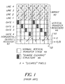
- the fast-dump structure is typically used within prior art devices in the transition area between the vertical and horizontal CCD.
- the fast-dump can be used to selectively dump charge from the main array of the device before transfer is made into the horizontal register for effective and fast subsampling of the image.
- These structures can be located at every column of the vertical section, or only at specific locations, (i.e., specific rows and/or columns), as predetermined at the time of design as described in U.S. Patent No. 5,440,343.
- prior art devices typically require a contact be made directly to the drain regions of each such structure, thereby putting obvious limitations on the cell sizes that can be realized for a given set of design rules.
- the fast-dump structure is typically used within prior art devices in the transition area between the vertical and horizontal CCD as shown in Fig. 1.
- the fast dump can be used to selectively dump charge from the main array of the device before transfer is made into the horizontal register for effective and fast subsampling of the image.
- These structures can be located at every column of the vertical imaging section, or only at specific locations, (i.e., specific rows and/or columns), as predetermined at the time of design as described in U.S. Patent No. 5,440,343.
- prior art devices typically require a contact be made directly to the drain regions of each such structure, thereby putting obvious limitations on the cell sizes that can be realized for a given set of design rules.
- other types of fast-dump structures exist that eliminate the need for a separate contact at each column, such as shown in Fig. 2, these structures have the disadvantage that charge must be transferred through the horizontal shift register which slows down the process.
- the primary advantage of this new structure is that it does not require a separate contact to its drain region by using the existing drain of a lateral-overflow drain (LOD) antiblooming structure that is also typically used on full-frame CCD image sensors.
- LOD lateral-overflow drain
- a separate opening in the gate electrode for the drain contact is avoided, thereby making the structure more compact.
- Gate control is provided by etching a hole in the CCD gate electrode over particular overflow channel regions of the LOD structure, and overlaying this with one of the subsequent gate electrode layers. This subsequent gate electrode is then used to control the fast-dump operation.
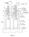
- the top view, cross-sectional views, and timing diagram for such a structure are shown in Figs. 4 and 5a-5d. Although timing is shown for a two-phase CCD being operated with accumulation-mode clocking, it is to be understood that other types of CCDs and clocking schemes may be used.
- Another advantage of this structure is that it does not require any additional masking or processing steps when built using a double (or more) electrode CCD process that employs a typical LOD structure.
- the fast-dump structure is typically used within prior art devices in the transition area between the vertical and horizontal CCD as shown in Fig. 1.
- the fast dump can be used to selectively dump charge from the main array of the device before transfer is made into the horizontal register for effective and fast subsampling of the image.
- These structures can be located at every column of the vertical imaging section, or only at specific locations, (i.e., specific rows and/or columns), as predetermined at the time of design as described in U.S. Patent No. 5,440,343.
- prior art devices typically require a contact be made directly to the drain regions of each such structure, thereby putting obvious limitations on the cell sizes that can be realized for a given set of design rules.
- FDG fast-dump gate
- Fig. 2b Illustrative examples of such devices are shown in Fig. 2b, and the prior art device as seen in Fig. 2a. These structures have the disadvantage that charge must be transferred through the horizontal shift register (H1, H2) which slows down the process.
- H1, H2 horizontal shift register
- multiple phase includes both two-phase and virtual-phase devices as well as devices having more than two phases.
- a virtual-phase device has one clocked phase and one virtual (non-clocked) phase BR1A and BR2A which refer to barrier implants.
- image sensing device 10 has a plurality of pixels 12 arranged in an array of rows 14 and columns 16.
- the image sensing device 10 is a two-phase, full-frame device with columns 16 formed as vertical charge-coupled device shift registers 18.
- Each of the vertical shift registers 18 has multiple pixels 12 with multiple phases 23 for each of the pixels 12.
- the preferred embodiment employs full-frame devices as image sensing device 10, because of the inherent advantages for the best mode being a full-frame device.
- the present invention could also be employed on interline-type devices.
- Fig. 3 illustrates a two-phase device employed by the preferred embodiment of the present invention having separate phase electrodes ⁇ 1 , ⁇ 2 within each of the CCD pixels 12.
- the phase electrodes ⁇ 1 , ⁇ 2 are electrically connected to voltage sources V1, V2, respectively, to provide alternate pulses to the two phases within the pixels 12 to effect charge transfer within each of the vertical shift register 18 two-phase CCD devices.
- Each of the phase electrodes ⁇ 1 , ⁇ 2 for the multiple phases 23 is formed from a separate electrode material resulting in two levels of electrode material.
- the phase electrodes ⁇ 1 , ⁇ 2 are shown such that adjacent electrodes overlap.
- phase electrodes ⁇ 1 , ⁇ 2 are formed from polysilicon, however, there are numerous teachings within the art wherein at least one of the phase electrodes ⁇ 1 , ⁇ 2 is formed from a different material, such as Indium Tin Oxide (ITO).
- ITO Indium Tin Oxide
- the fast-dump gate 30 of the present invention is formed at strategic locations within selected CCD pixels 12 by first forming a hole within one of the phase electrodes ⁇ 1 , ⁇ 2 within the selected CCD pixels 12. A drain is formed adjacent to the hole to provide for the removal of pixel charges from the selected cells 22 of the vertical CCD shift register 18 which allows for altering the resolution size.
- the capability for altering resolution sizes is desired in numerous applications such as higher speed applications or for windowing applications where only a subset of the entire pixel array of the image sensing device 10 is desired. In a reduced resolution mode, it is not necessary to output all of the pixel charges through horizontal shift register 40.
- a fast-dump gate electrode 30 is formed to remove undesired pixel data as expeditiously as possible by forming an electrode within the hole adjacent to a drain.
- the electrode is formed from a different electrode level from that in which the hole is formed allowing control over the draining of pixel charges without effecting the charge transfer within the vertical CCD shift register 18.
- the CCD is a two-phase device, having two levels of electrode material (polysilicon, ITO or other electrode material).
- the hole within the preferred embodiment is formed in the first electrode level and the fast-dump gate electrode 30 is then formed over the hole from the second level of electrode material. This allows the fast-dump gate electrode 30 to be isolated from the first electrode level in which it is formed enabling independent operation of the fast-dump gate electrode 30 without effecting the operation of the vertical CCD shift register 18.
- the fast-dump gate electrode 30 within the preferred embodiment is formed in corresponding cells 22 within each of the columns 16 of the CCD such that an entire row of pixels can be drained from the charge coupled devices.
- the drain used to form the fast-dump gate is a lateral overflow drain structure and the CCD is preferably a full-frame device.
- Fig. 4 is a top view of a portion of image sensing device 10 that has been selected to show the features and structure of the new fast-dump gate 30.
- the phase-1 electrode ⁇ 1 is electrically connected to voltage source V1
- the phase-2 electrode ⁇ 2 is electrically connected to voltage source V2 to create the two-phase, image sensing device 10 of the preferred embodiment.
- the fast-dump gate 30 electrode is preferably formed within the phase-1 electrode ⁇ 1 area because this is the last phase in the cell which facilitates an efficient dump of all the charge contained within a cell. While it will be understood to those skilled in the art, that the fast-dump gate 30 can be formed in any of the phases, it is preferably formed within the last phase of the cell.
- phase-1 electrode ⁇ 1 is drained via the fast-dump gate 30 prior to charge from the phase-2 electrode ⁇ 2 being shifted into the phase-1 electrode ⁇ 1 area where this charge is also drained via fast-dump gate 30.
- the organization of having the last phase contain fast-dump gate 30 is consistent before charge is transferred out of the cell, and it is desirable to remove all the charge from the cell via the fast-dump gate 30 structure. Therefore, the last phase within a cell is the preferred phase for placement of the fast-dump gate 30 structure.
- the frame transfer, image sensing device 10 has the fast-dump gate 30 structure formed within cell 32 that consists of two phases as previously discussed.
- Each of the columns 16 within sensing has a lateral overflow drain (LOD) 52 on one side of the column 16 that, within the preferred embodiment, is formed from an n+ material.
- LOD lateral overflow drain
- a channel stop 54 is formed from a p+ material.
- the columns 16 have the LOD 52 and channel stop 54 formed within a p-type epitaxial layer formed on a p-type substrate.
- An n-type buried channel 42 is formed within the portions of the column 16 that is intended to transfer charge through the various phases.
- the n-type buried channel 42 will exist throughout the image sensor device 10 except in the areas that are adjacent LOD 52 and the junction edges of the phase electrodes ⁇ 1 , ⁇ 2 . Therefore, fingers of the n-type channel 42 will reach the n+ type LOD 52 in the center areas of the phase electrodes ⁇ 1 , ⁇ 2 as seen in Fig. 4. In the cells where the fast-dump gates 30 are formed, a trench is formed in the center of the phase electrode over the finger of n-type buried channel 42 that extends towards LOD 52 as seen in Fig. 4.
- Fig. 5a is a cross-sectional view taken through line A-A of Fig. 4 wherein the p-type barrier implant 56 is shown beneath notch 58.
- This p-type barrier implant 56 is along the edge of column 16 near LOD 52.
- Fig. 5b is a cross-sectional view taken through line B-B of Fig. 4 illustrating the entire width of a phase not having a fast-dump gate 30.
- notch 58 illustrated in Fig. 5a contained in the phase having a fast-dump gate 30 are both of these figures.
- Both of these figures contain the p-type barrier implant 56 that provides a threshold for charges to the LOD 52.
- Fig. 5c is a cross-sectional view of line C-C of Fig. 4 illustrating a typical charge transfer path for one of the columns including a phase having a fast-dump gate 30.
- Fig. 5c is a view directly through notch 58 to illustrate the formation of the fast-dump gate 30 structure of the present invention in conjunction with the previously discussed Fig. 5a.
- Various fingers like outcrops of n-type buried channel 42 can be seen within each of the phases beneath the center of each electrode embedded within the a p-type barrier implant layer 56.
- the p-type barrier implant 56 that runs along the entire column is evident within Fig. 5c.
- the fast-dump gate 30 in the preferred embodiment is placed directly on top of the n-type buried channel 42 outcrops for the phase selected to contained the fast-dump gate 30.
- Fig. 5d which is a cross-sectional view through line D-D of Fig. 4. This cross section illustrates the structure of the preferred embodiment along a line parallel to that discussed above for Fig. 5c only farther towards the center of each of the charge transfer cells.
- P-type barrier implants 65 are placed at the edge of each the electrodes to provide a potential threshold between each of the phases.
- Fig. 6a is a sample timing diagram for the fast-dump structure of Fig. 4.
- Fig. 6b is a channel potential diagram for the fast-dump structure of Fig. 4 illustrating the operation of the fast-dump gate 30 wherein the charges contained in that phase get dumped into the lateral overflow drain 52.
- fast-dump gate 30 provides a structure that does not require a separate contact to a drain region instead using the existing drain of a lateral-overflow drain (LOD) typically used for antiblooming purposes.
- LOD structures are typically used on full-frame CCD image sensors.
- Gate control is provided by etching a hole in the CCD gate electrode over the overflow channel region of the LOD structure, and overlaying this with one of the subsequent gate electrode layers. This subsequent gate electrode is then used to control the fast-dump operation.
- FIG. 4 The top view, cross-sectional views, and timing diagram for such a structure are shown in Figs. 4 through 6b. Although timing is shown for a two-phase CCD being operated with accumulation-mode clocking, it is to be understood that other types of CCDs and clocking schemes may be used.
- Another advantage of this structure is that it does not require any additional masking or processing steps when built using a double (or more) electrode CCD process that employs a typical LOD structure.
Landscapes
- Solid State Image Pick-Up Elements (AREA)
- Transforming Light Signals Into Electric Signals (AREA)
- Facsimile Heads (AREA)
Abstract
Description
Claims (10)
- An image sensing device comprising:a plurality of pixels arranged in an array of rows and columns;a plurality of vertical charge coupled device shift registers used to form the columns, the vertical charge coupled devices defining the pixels where each of the pixels have multiple phases;a plurality of electrodes formed upon the image sensing device such that there is at least one electrode for each pixel;a hole being formed within the electrode of at least one of the pixels, the hole having a dump electrode formed therein, the dump electrode being formed from a subsequent level of electrode material from the electrode containing the hole; anda drain adjacent to pixel wherein the dump electrode is operatively connected to a drain.
- The image sensing device of claim 1 wherein the drain structure is a lateral overflow drain structure buried within the substrate.
- The image sensing device of claim 1 wherein the hole is formed over a barrier implanted region.
- The image sensing device of claim 1 wherein the image sensing device is a full frame charge coupled device.
- The image sensing device of claim 1 wherein the image sensing device is a full frame device formed within a substrate of a first conductivity having a buried channel of a second conductivity of opposite polarity from the first conductivity.
- An image sensing device comprising:a plurality of pixels arranged in an array of rows and columns;a plurality of vertical charge coupled device shift registers used to form the columns, the vertical charge coupled devices defining the pixels where each of the pixels have multiple phases;a plurality of electrodes formed upon the image sensing device such that there is at least one electrode for each of the phases within the pixels;a hole being formed within the electrode of at least one of the pixels, the hole having a dump electrode formed therein, the dump electrode being formed from a subsequent level of electrode material from the electrode containing the hole; anda drain adjacent to pixel wherein the dump electrode is operatively connected to a drain.
- The image sensing device of claim 6 wherein the drain structure is a lateral overflow drain structure buried within the substrate.
- The image sensing device of claim 6 wherein the hole is formed over a barrier implanted region.
- The image sensing device of claim 6 wherein the image sensing device is a full frame charge coupled device.
- The image sensing device of claim 6 wherein the image sensing device is a full frame device formed within a substrate of a first conductivity having a buried channel of a second conductivity of opposite polarity from the first conductivity.
Applications Claiming Priority (2)
| Application Number | Priority Date | Filing Date | Title |
|---|---|---|---|
| US533051 | 2000-03-22 | ||
| US09/533,051 US6693671B1 (en) | 2000-03-22 | 2000-03-22 | Fast-dump structure for full-frame image sensors with lod antiblooming structures |
Publications (3)
| Publication Number | Publication Date |
|---|---|
| EP1137071A2 true EP1137071A2 (en) | 2001-09-26 |
| EP1137071A3 EP1137071A3 (en) | 2005-09-14 |
| EP1137071B1 EP1137071B1 (en) | 2010-09-01 |
Family
ID=24124256
Family Applications (1)
| Application Number | Title | Priority Date | Filing Date |
|---|---|---|---|
| EP01200931A Expired - Lifetime EP1137071B1 (en) | 2000-03-22 | 2001-03-12 | Fast-dump structure for full-frame image sensors with lateral overflow drain antiblooming structures |
Country Status (4)
| Country | Link |
|---|---|
| US (1) | US6693671B1 (en) |
| EP (1) | EP1137071B1 (en) |
| JP (1) | JP4743983B2 (en) |
| DE (1) | DE60142943D1 (en) |
Cited By (5)
| Publication number | Priority date | Publication date | Assignee | Title |
|---|---|---|---|---|
| EP1195817A2 (en) | 2000-09-12 | 2002-04-10 | Eastman Kodak Company | Method for reducing dark current in charge coupled devices |
| WO2006026434A1 (en) * | 2004-08-27 | 2006-03-09 | Eastman Kodak Company | Fast flush structure for image sensors |
| WO2009137079A1 (en) * | 2008-05-09 | 2009-11-12 | Eastman Kodak Company | Draining residual charge from (ccd) shift registers |
| CN105611197A (en) * | 2015-12-23 | 2016-05-25 | 中国科学院长春光学精密机械与物理研究所 | Anti-saturation read method of overflow-resistant function-free frame transfer CCD |
| EP4468359A4 (en) * | 2022-02-24 | 2026-01-07 | Hamamatsu Photonics Kk | SOLID BODY IMAGE ELEMENT |
Families Citing this family (10)
| Publication number | Priority date | Publication date | Assignee | Title |
|---|---|---|---|---|
| JP2001238134A (en) * | 2000-02-23 | 2001-08-31 | Sony Corp | Solid-state imaging device, driving method thereof, and camera system |
| US20050068441A1 (en) * | 2003-09-26 | 2005-03-31 | Eastman Kodak Company | Multiple output CCD for color imaging |
| US20080007622A1 (en) * | 2006-06-08 | 2008-01-10 | Eastman Kodak Company | Method of improving solid-state image sensor sensitivity |
| JP2009177018A (en) * | 2008-01-25 | 2009-08-06 | Sanyo Electric Co Ltd | Solid-state imaging device and manufacturing method thereof |
| US8772891B2 (en) | 2008-12-10 | 2014-07-08 | Truesense Imaging, Inc. | Lateral overflow drain and channel stop regions in image sensors |
| JP5243983B2 (en) * | 2009-01-30 | 2013-07-24 | 浜松ホトニクス株式会社 | Solid-state image sensor with built-in electron multiplication function |
| JP5300577B2 (en) * | 2009-04-23 | 2013-09-25 | 三菱電機株式会社 | TDI image sensor and method for driving the image sensor |
| US8773563B2 (en) | 2011-05-25 | 2014-07-08 | Truesense Imaging, Inc. | Multi-purpose architecture for CCD image sensors |
| US8800130B2 (en) | 2011-05-25 | 2014-08-12 | Truesense Imaging, Inc. | Methods for producing image sensors having multi-purpose architecture |
| US9049353B2 (en) | 2011-09-28 | 2015-06-02 | Semiconductor Components Industries, Llc | Time-delay-and-integrate image sensors having variable integration times |
Family Cites Families (18)
| Publication number | Priority date | Publication date | Assignee | Title |
|---|---|---|---|---|
| JPS5817788A (en) * | 1981-07-23 | 1983-02-02 | Toshiba Corp | Solid-state image pickup device |
| US4528596A (en) * | 1982-11-30 | 1985-07-09 | Rca Corporation | Suppression of edge effects arising in CCD imager field registers |
| US4611140A (en) | 1985-08-26 | 1986-09-09 | The United States Of America As Represented By The Secretary Of The Navy | Saw-CTD parallel to serial imager |
| US4908684A (en) * | 1986-07-07 | 1990-03-13 | Hitachi, Ltd. | Solid-state imaging device |
| US4972254A (en) * | 1987-02-24 | 1990-11-20 | Kabushiki Kaisha Toshiba | Solid state image sensors for reproducing high definition images |
| US5121214A (en) | 1990-06-29 | 1992-06-09 | The United States Of America As Represented By The United States Department Of Energy | Method for eliminating artifacts in CCD imagers |
| US5130774A (en) * | 1990-07-12 | 1992-07-14 | Eastman Kodak Company | Antiblooming structure for solid-state image sensor |
| WO1992021151A2 (en) | 1991-05-10 | 1992-11-26 | Q-Dot, Inc. | HIGH-SPEED PERISTALTIC CCD IMAGER WITH GaAs FET OUTPUT |
| US5355165A (en) | 1992-08-06 | 1994-10-11 | Princeton Scientific Instruments, Inc. | Very high frame rate CCD imager |
| US5343297A (en) | 1992-09-17 | 1994-08-30 | General Electric Company | Charge amplifier with precise, integer gain |
| US5440343A (en) | 1994-02-28 | 1995-08-08 | Eastman Kodak Company | Motion/still electronic image sensing apparatus |
| US5668597A (en) | 1994-12-30 | 1997-09-16 | Eastman Kodak Company | Electronic camera with rapid automatic focus of an image upon a progressive scan image sensor |
| EP0756759B1 (en) * | 1995-02-21 | 2004-04-14 | Dalsa Corporation | Charge-coupled imaging device |
| JP3590944B2 (en) * | 1996-02-23 | 2004-11-17 | 日本テキサス・インスツルメンツ株式会社 | Charge-coupled semiconductor device |
| JP3750221B2 (en) * | 1996-10-01 | 2006-03-01 | ソニー株式会社 | Solid-state imaging device |
| JP2894323B2 (en) * | 1997-06-23 | 1999-05-24 | 日本電気株式会社 | Solid-state imaging device and method of manufacturing the same |
| US6051857A (en) * | 1998-01-07 | 2000-04-18 | Innovision, Inc. | Solid-state imaging device and method of detecting optical signals using the same |
| JP2000134540A (en) * | 1998-10-29 | 2000-05-12 | Nec Corp | Solid-state image pickup device and its driving method |
-
2000
- 2000-03-22 US US09/533,051 patent/US6693671B1/en not_active Expired - Lifetime
-
2001
- 2001-03-12 EP EP01200931A patent/EP1137071B1/en not_active Expired - Lifetime
- 2001-03-12 DE DE60142943T patent/DE60142943D1/en not_active Expired - Lifetime
- 2001-03-21 JP JP2001081327A patent/JP4743983B2/en not_active Expired - Lifetime
Cited By (9)
| Publication number | Priority date | Publication date | Assignee | Title |
|---|---|---|---|---|
| EP1195817A2 (en) | 2000-09-12 | 2002-04-10 | Eastman Kodak Company | Method for reducing dark current in charge coupled devices |
| EP1195817A3 (en) * | 2000-09-12 | 2008-04-09 | Eastman Kodak Company | Method for reducing dark current in charge coupled devices |
| WO2006026434A1 (en) * | 2004-08-27 | 2006-03-09 | Eastman Kodak Company | Fast flush structure for image sensors |
| US7492404B2 (en) | 2004-08-27 | 2009-02-17 | Eastman Kodak Company | Fast flush structure for solid-state image sensors |
| WO2009137079A1 (en) * | 2008-05-09 | 2009-11-12 | Eastman Kodak Company | Draining residual charge from (ccd) shift registers |
| US8134630B2 (en) | 2008-05-09 | 2012-03-13 | Truesense Imaging, Inc. | System and method for draining residual charge from charge-coupled device (CCD) shift registers in image sensors having reset drains |
| CN102017155B (en) * | 2008-05-09 | 2013-07-17 | 储赛思成像有限公司 | Drain remaining charge from (CCD) shift register |
| CN105611197A (en) * | 2015-12-23 | 2016-05-25 | 中国科学院长春光学精密机械与物理研究所 | Anti-saturation read method of overflow-resistant function-free frame transfer CCD |
| EP4468359A4 (en) * | 2022-02-24 | 2026-01-07 | Hamamatsu Photonics Kk | SOLID BODY IMAGE ELEMENT |
Also Published As
| Publication number | Publication date |
|---|---|
| DE60142943D1 (en) | 2010-10-14 |
| EP1137071A3 (en) | 2005-09-14 |
| EP1137071B1 (en) | 2010-09-01 |
| US6693671B1 (en) | 2004-02-17 |
| JP2001326344A (en) | 2001-11-22 |
| JP4743983B2 (en) | 2011-08-10 |
Similar Documents
| Publication | Publication Date | Title |
|---|---|---|
| EP1137071B1 (en) | Fast-dump structure for full-frame image sensors with lateral overflow drain antiblooming structures | |
| US4168444A (en) | Imaging devices | |
| US5130774A (en) | Antiblooming structure for solid-state image sensor | |
| JPS62265759A (en) | Solid state image pickup element | |
| US5402459A (en) | Frame transfer image sensor with electronic shutter | |
| EP0764987A2 (en) | Rapid-sequence full-frame CCD sensor | |
| US5235196A (en) | Transfer region design for charge-coupled device image sensor | |
| KR101159032B1 (en) | Solid-state imaging device | |
| US6114717A (en) | Solid-state imaging device having no transfer error of the signal charges from vertical horizontal charge-transfer section | |
| EP1289020B1 (en) | A lateral overflow drain, antiblooming structure for CCD devices having improved breakdown voltage | |
| US4974043A (en) | Solid-state image sensor | |
| EP1406305B1 (en) | Method of operating a charge-coupled device (CCD) | |
| US5256891A (en) | CCD electrode structure for image sensors | |
| EP0059547B1 (en) | Clock controlled anti-blooming for virtual phase ccd's | |
| JP2699841B2 (en) | Solid-state imaging device | |
| US4654683A (en) | Blooming control in CCD image sensors | |
| US5134087A (en) | Fabricating a two-phase CCD imager cell for TV interlace operation | |
| EP0614225B1 (en) | Charge coupled device | |
| US4207477A (en) | Bulk channel CCD with switchable draining of minority charge carriers | |
| US20040095491A1 (en) | Solid state imaging device with lateral overflow drain and driving method thereof achieving low power consumption | |
| JP2877047B2 (en) | Solid-state imaging device | |
| JPH08264747A (en) | Solid-state imager with container lateral overflow drain implant and method of making same | |
| JP3301176B2 (en) | Charge transfer device | |
| JP3247163B2 (en) | Solid-state imaging device and manufacturing method thereof | |
| JP2002076318A (en) | Solid-state imaging device |
Legal Events
| Date | Code | Title | Description |
|---|---|---|---|
| PUAI | Public reference made under article 153(3) epc to a published international application that has entered the european phase |
Free format text: ORIGINAL CODE: 0009012 |
|
| AK | Designated contracting states |
Kind code of ref document: A2 Designated state(s): AT BE CH CY DE DK ES FI FR GB GR IE IT LI LU MC NL PT SE TR |
|
| AX | Request for extension of the european patent |
Free format text: AL;LT;LV;MK;RO;SI |
|
| PUAL | Search report despatched |
Free format text: ORIGINAL CODE: 0009013 |
|
| AK | Designated contracting states |
Kind code of ref document: A3 Designated state(s): AT BE CH CY DE DK ES FI FR GB GR IE IT LI LU MC NL PT SE TR |
|
| AX | Request for extension of the european patent |
Extension state: AL LT LV MK RO SI |
|
| 17P | Request for examination filed |
Effective date: 20060307 |
|
| AKX | Designation fees paid |
Designated state(s): DE FR GB NL |
|
| GRAP | Despatch of communication of intention to grant a patent |
Free format text: ORIGINAL CODE: EPIDOSNIGR1 |
|
| GRAS | Grant fee paid |
Free format text: ORIGINAL CODE: EPIDOSNIGR3 |
|
| GRAA | (expected) grant |
Free format text: ORIGINAL CODE: 0009210 |
|
| AK | Designated contracting states |
Kind code of ref document: B1 Designated state(s): DE FR GB NL |
|
| REG | Reference to a national code |
Ref country code: GB Ref legal event code: FG4D |
|
| REF | Corresponds to: |
Ref document number: 60142943 Country of ref document: DE Date of ref document: 20101014 Kind code of ref document: P |
|
| REG | Reference to a national code |
Ref country code: NL Ref legal event code: T3 |
|
| PLBE | No opposition filed within time limit |
Free format text: ORIGINAL CODE: 0009261 |
|
| STAA | Information on the status of an ep patent application or granted ep patent |
Free format text: STATUS: NO OPPOSITION FILED WITHIN TIME LIMIT |
|
| 26N | No opposition filed |
Effective date: 20110606 |
|
| REG | Reference to a national code |
Ref country code: GB Ref legal event code: 732E Free format text: REGISTERED BETWEEN 20120315 AND 20120321 |
|
| REG | Reference to a national code |
Ref country code: DE Ref legal event code: R097 Ref document number: 60142943 Country of ref document: DE Effective date: 20110606 |
|
| PGFP | Annual fee paid to national office [announced via postgrant information from national office to epo] |
Ref country code: NL Payment date: 20140308 Year of fee payment: 14 |
|
| PGFP | Annual fee paid to national office [announced via postgrant information from national office to epo] |
Ref country code: FR Payment date: 20140311 Year of fee payment: 14 |
|
| PGFP | Annual fee paid to national office [announced via postgrant information from national office to epo] |
Ref country code: GB Payment date: 20140312 Year of fee payment: 14 |
|
| REG | Reference to a national code |
Ref country code: DE Ref legal event code: R082 Ref document number: 60142943 Country of ref document: DE Representative=s name: MEYER & PARTNER GBR, DE |
|
| REG | Reference to a national code |
Ref country code: GB Ref legal event code: 732E Free format text: REGISTERED BETWEEN 20140904 AND 20140910 |
|
| REG | Reference to a national code |
Ref country code: DE Ref legal event code: R082 Ref document number: 60142943 Country of ref document: DE Representative=s name: MEYER & PARTNER GBR, DE Effective date: 20140918 Ref country code: DE Ref legal event code: R081 Ref document number: 60142943 Country of ref document: DE Owner name: SEMICONDUCTOR COMPONENTS INDUSTRIES, LLC (N. D, US Free format text: FORMER OWNER: EASTMAN KODAK CO., ROCHESTER, N.Y., US Effective date: 20140918 |
|
| REG | Reference to a national code |
Ref country code: NL Ref legal event code: SD Effective date: 20150209 Ref country code: NL Ref legal event code: TD Effective date: 20150209 |
|
| GBPC | Gb: european patent ceased through non-payment of renewal fee |
Effective date: 20150312 |
|
| REG | Reference to a national code |
Ref country code: NL Ref legal event code: MM Effective date: 20150401 |
|
| REG | Reference to a national code |
Ref country code: FR Ref legal event code: ST Effective date: 20151130 |
|
| PG25 | Lapsed in a contracting state [announced via postgrant information from national office to epo] |
Ref country code: GB Free format text: LAPSE BECAUSE OF NON-PAYMENT OF DUE FEES Effective date: 20150312 |
|
| PG25 | Lapsed in a contracting state [announced via postgrant information from national office to epo] |
Ref country code: FR Free format text: LAPSE BECAUSE OF NON-PAYMENT OF DUE FEES Effective date: 20150331 |
|
| PG25 | Lapsed in a contracting state [announced via postgrant information from national office to epo] |
Ref country code: NL Free format text: LAPSE BECAUSE OF NON-PAYMENT OF DUE FEES Effective date: 20150401 |
|
| PGFP | Annual fee paid to national office [announced via postgrant information from national office to epo] |
Ref country code: DE Payment date: 20200218 Year of fee payment: 20 |
|
| REG | Reference to a national code |
Ref country code: DE Ref legal event code: R071 Ref document number: 60142943 Country of ref document: DE |