EP1134844A1 - Electrical connector with low-inductance terminal structure - Google Patents
Electrical connector with low-inductance terminal structure Download PDFInfo
- Publication number
- EP1134844A1 EP1134844A1 EP00105530A EP00105530A EP1134844A1 EP 1134844 A1 EP1134844 A1 EP 1134844A1 EP 00105530 A EP00105530 A EP 00105530A EP 00105530 A EP00105530 A EP 00105530A EP 1134844 A1 EP1134844 A1 EP 1134844A1
- Authority
- EP
- European Patent Office
- Prior art keywords
- contact portion
- bump
- slit
- electrical connector
- terminal
- Prior art date
- Legal status (The legal status is an assumption and is not a legal conclusion. Google has not performed a legal analysis and makes no representation as to the accuracy of the status listed.)
- Withdrawn
Links
Images


Classifications
-
- H—ELECTRICITY
- H01—ELECTRIC ELEMENTS
- H01R—ELECTRICALLY-CONDUCTIVE CONNECTIONS; STRUCTURAL ASSOCIATIONS OF A PLURALITY OF MUTUALLY-INSULATED ELECTRICAL CONNECTING ELEMENTS; COUPLING DEVICES; CURRENT COLLECTORS
- H01R12/00—Structural associations of a plurality of mutually-insulated electrical connecting elements, specially adapted for printed circuits, e.g. printed circuit boards [PCB], flat or ribbon cables, or like generally planar structures, e.g. terminal strips, terminal blocks; Coupling devices specially adapted for printed circuits, flat or ribbon cables, or like generally planar structures; Terminals specially adapted for contact with, or insertion into, printed circuits, flat or ribbon cables, or like generally planar structures
- H01R12/70—Coupling devices
- H01R12/71—Coupling devices for rigid printing circuits or like structures
- H01R12/72—Coupling devices for rigid printing circuits or like structures coupling with the edge of the rigid printed circuits or like structures
- H01R12/721—Coupling devices for rigid printing circuits or like structures coupling with the edge of the rigid printed circuits or like structures cooperating directly with the edge of the rigid printed circuits
Definitions
- the present invention relates to the art of electrical connectors and particularly to the terminal structure of a card edge connector.
- Card edge connectors are widely used in electronic devices utilizing circuit boards. Typically, such connectors are used for mounting a daughter circuit board or an interface card to a primary circuit board.
- the connector includes an elongated insulative housing which forms a slot dimensioned to receive an edge of the daughter circuit board.
- the daughter circuit board may be, for example, a memory module, interface card, or some other auxiliary circuit card.
- the housing includes a plurality of conductive terminals with contact portions located in the slot for contacting correspondingly located contact pads on the daughter circuit board.
- the housing is mounted to the primary circuit board so that tail ends of the conductive terminals, which extend from a bottom of the housing, are held in electrical contact with respective electrical contacts on the primary circuit board.
- the terminals of such known connectors have been made from a sheet, whereby the contact portions are formed to have a V-shaped bend. Each of the terminals is intended to resiliently contact against a the circuit board at the apex of the V-shaped bend.
- these conventional types of terminals in such connectors have exhibited high inductive reactance, especially for high signal frequencies. More specifically, this undesirable characteristic is attributable to the bent shape of the terminals, whereby each of the terminals has a greater total length than its height dimension within the slot. Connectors with such known terminal structures may be unsuitable for high frequency applications.
- the present invention provides an improved connector that has low inductance characteristics.
- a connector according to the invention can advantageously be used in high frequency applications.
- an electrical connector for connecting an electrical component to a primary circuit board.
- the connector includes a housing having a horizontal base, a plurality of walls extending from the base and defining a longitudinal slot for receiving the electrical component, the walls further defining a plurality of terminal cavities adjacent to the slot.
- the connector further includes a plurality of conductive terminals, each of the conductive terminals having a tail portion extending from the base and a resilient contact portion that generally resides in a respective one of the terminal cavities.
- the contact portion has a generally planar body which, in an unmated condition, extends generally vertically within the terminal cavity. Also, the contact portion has a bump formed in the body that projects inwardly into the slot.
- the bump is disposed near an upper end of the contact portion.
- the contact portion includes a vertical slit, the contact portion being bent on one side of the slit to form the bump.
- the slit terminates below an upper end of the contact portion so that an upper end of the bump is unitarily connected to a flat side opposite the slit.
- the slit extends to an upper end of the contact portion so that an upper end of the bump is free relative to the flat side opposite the slit.
- the bump is press-formed with bend angles that provide a low moment arm from a crest or apex of the bump relative to a lower bend of the bump.
- the bump is relatively rigid, deflecting little relative to the remainder of the generally flat terminal during use.
- the planar portion of the contact portion extending from the base of the terminal is relatively resilient and deflectable.
- An advantage of the present invention is to provide an improved electrical connector for receiving an electrical component.
- Another advantage of the present invention is to provide an electrical connector that has low inductance and high efficiency.
- a further advantage of the present invention is to provide an electrical connector that can be used to transfer high frequency signals.
- Yet another advantage of the present invention is to provide an electrical connector that is simple and inexpensive to manufacture.
- a still further advantage of the present invention is to provide an electrical connector having conductive terminals with reduced amounts of material.
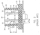
- FIGS. 1 and 2 illustrate a prior art connector
- FIG. 1 is a perspective view of a prior art connector illustrating in section a portion of the connector with terminals exploded therefrom, a remainder of a housing of the connector being illustrated in phantom. The terminals are shown prior to removal from a strip that remains of a blank from which the terminals may be manufactured.
- FIG. 2 is a sectional view of the prior art connector of FIG. 1.
- FIGS. 3-5 illustrate a connector and terminals according to an embodiment of the invention.
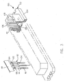
- FIG. 3 is a perspective view of a connector according to an embodiment of the invention illustrating in section a portion of the connector with terminals exploded therefrom, a remainder of a housing of the connector being illustrated in phantom. The terminals are shown prior to removal from a strip that remains of a blank from which the terminals may be manufactured.
- FIG. 4 is a perspective view of an individual terminal according to an embodiment of the present invention.
- FIG. 5 is a side view of the terminal of FIG. 4.
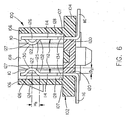
- FIG. 6 is a sectional view of a connector according to an embodiment of the present invention wherein terminals of the type illustrated in FIGS. 3-5 are installed.
- FIGS. 7-10 illustrate a connector and terminals according to another embodiment of the invention.
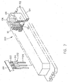
- FIG. 7 is a perspective view of a connector according to an embodiment of the invention illustrating, in section, an end portion of the connector with terminals exploded therefrom, a remainder of a housing of the connector being illustrated in phantom. The terminals are shown prior to removal from a strip that remains of a blank from which the terminals may be manufactured.
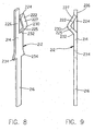
- FIG. 8 is a perspective view of an individual terminal according to an embodiment of the present invention.
- FIG. 9 is a side view of the terminal of FIG. 8.
- FIG. 10 is a sectional view of a connector according to an embodiment of the present invention wherein terminals of the type illustrated in FIGS. 7-9 are installed.
- FIGS. 1 and 2 illustrate a conventional card edge connector 20 configured to receive a daughter circuit board (not shown), otherwise referred to herein as a circuit card or interface card.
- a circuit card or interface card As is known, such a card has a plurality of contact pads disposed along both sides of an edge thereof.
- the embodiments herein are directed to a card edge connector, it is contemplated that the same terminal structure can be applied to other types of electrical connectors such as a connector that receives a portion of a second connector therein.
- the conventional connector 20 includes a housing 22, a base 24, a plurality of upright walls 26 forming a central insertion slot 28 extending lengthwise in the housing 22, and a plurality of evenly-spaced terminal cavities 30 recessed into the walls 28 along both sides of the central insertion slot 28.
- the conventional connector 20 includes a plurality of conductive terminals 32. To accommodate the terminals 32, the connector 20 has a plurality of through holes 34 extending through the base 24 from a bottom of the housing 22. Each of the terminal cavities 30 and through holes 34 is shaped to receive a respective one of the terminals 32, as shown in FIG. 2.
- the conventional conductive terminals 32 are made from a metal sheet.
- the illustration in FIG. 2 shows a plurality of the terminals 32 still unitarily attached to a strip 37 remaining from original metal sheet stock.
- each of the terminals is formed to include a resilient contact portion 36 shaped with a V-shaped bend 40.
- the terminals 32 are cut free of the strip 37 when mounted to the housing 22.
- the contact portion 36 extends from a tail portion 38 fixedly mounted to the base 24 and extending through the hole 34.
- the V-shaped bend 40 is conventionally formed in the contact portion 36 to define a lower, angled leg 42 so that the terminal 32 provides desired resilient contact behavior. Particularly, when the tail portion 38 of the terminal 32 is mounted, as shown in FIG.
- the V-shaped contact portion 36 assumes an inner position away from an inner wall of the slot 28.
- the lower angled leg 42 of the resilient contact portion 36 deflects to accommodate the interface card, creating a torque around the vertical part 44 of the tail portion 38 mounted to the base 24.
- the inwardly projecting end 40 of the V-shaped contact portion 36 contacts the corresponding contact pads on the circuit card.
- the V-shaped contact portion 36 of the conventional terminal 32 has a longer total current path length than its height dimension due in part to the relatively large height H 1 and depth D 1 of the displacement of the angled leg 42 between the apex of the projecting bend 40 and the vertical part 44 of the tail portion 38.
- This total current path length increases the inductance and signal delay through the terminal 32. It has been found that the inductive reactance is particularly large at high signal transmission speeds. Therefore, the connector having this conventional type of terminal structure can be unsuitable for high frequency applications.
- FIGS. 3 to 10 two exemplary embodiments of the present invention will be described.
- a first embodiment is shown in FIGS. 3-6, and a second embodiment is illustrated in FIGS. 7-10.
- the connector 100 includes an elongate housing 102 having a base 104 and a plurality of walls 106 extending upwardly from the base 104.
- the walls 106 define a central insertion slot 108 extending longitudinally in the housing 102, the slot 108 being shaped to receive an electrical component such as an edge of the circuit card or daughter circuit board.
- the housing 102 further has a plurality of terminal cavities 110 defined by recesses in the walls 106 along both sides of the interior of the slot 108.
- the connector 100 shown in FIGS. 3-6 includes a plurality of conductive terminals 112.
- Each of the conductive terminals 112 has a respective upper contact portion 114 and a lower tail portion 116.
- the contact portion 114 is generally flat or planar in shape.
- Each of the terminals 112 is mounted to the housing 102.
- the terminals 112 may include a pair of oppositely-extending projections 134 forming a downwardly-facing edge to securely retain the terminal 112 in the housing 102.
- the tail portion 116 extends through a through hole 120 in the base 104 of the housing 102, the tail portion 116 being securely fixed therein. Furthermore, in the illustrated embodiment, each of the tail portions 116 is bent outwardly to extend in a generally right angle for connection to the surface of a primary circuit board (not shown) such as by soldering. However, the tail portion may also have a through-hole configuration. Each of the contact portions 114 resides generally vertically within a respective one of the terminal cavities 110.
- the conductive terminals 112 are stamped and formed from a metal sheet.
- the illustration in FIG. 3 shows a plurality of the terminals 112 still unitarily attached to a strip 118 remaining from an original metal sheet.
- the terminals 112 are cut free of the strip 118 prior to assembly with the housing 102.
- the contact portion 114 extends generally vertically from the tail portion 116.
- each of the terminals 112 includes a bump 122 formed in an upper part of the generally planar contact portion 114.
- the bump 122 projects inwardly such that, when the terminal 112 is in an undeflected condition, the bump 122 resides slightly within the slot 108, as shown in FIG. 6.
- a vertical slit 124 is formed in the contact portion 114.
- a curved bend is pressed in the contact portion 114 on one side of the slit 124 to form the bump 122.
- the bump includes a lower leg 125 and an upper leg 127.
- the contact portion 114 has a planar side 126.
- the slit 124 terminates below an upper end of the contact portion 114 so that an upper end of the bump 122 is integral with the upper end of the planar side 126 of the contact portion 114 opposite the slit 124.
- the terminal 112 provides a primary current path "A" which goes down the lower leg 125 of the bump 122, through the contact portion 114 and down the tail portion 116.
- the unitary connection at the upper end of the terminal 112 between the bump 122 and the planar side 126 provides a secondary current path "B" up the upper leg 127 of the bump 122, down the planar side 126, through the contact portion 114 and down the tail portion 116.
- the secondary current path operates to reduce the inductance of the terminal.
- the resilient contact portions 114 Upon insertion of an interface card or other electrical component into the central slot 108, the resilient contact portions 114 deflect outwardly within the terminal cavities to accommodate the thickness of the card or component. More specifically, the resilient contact 114 portion of each terminal 112 deflects upon insertion of the electrical component, biasing the bump 122 in engagement against the corresponding contact.
- the terminal cavities 110 have a predetermined lateral depth such that a gap 128 (FIG. 6) is formed between the terminal 112 and the inner surface 107 of the housing wall 106 to permit deflection of the contact portion 114 of the terminal 112 in an outward direction, away from the slot 108.
- the height H 2 and depth D 2 of the lower leg 125 between an apex 130 of the bump 122 and a lower bend 132 at the vertical planar region of the contact portion 114 is significantly less than height H 1 and depth D 1 ,respectively, of the angled leg 42 in Figure 2.
- the apex 130 of the bump 122 is close to the lower bend 132 at a junction of the bump 122 and the planar region of the contact portion 114.
- the lower bend 132 preferably has an angle such that the apex 130 exerts a low moment arm around the lower bend 132, thereby avoiding much deflection of the bump 122 relative to the planar region of the contact portion 114. Accordingly, the bump 122 will not undesirably deflect, thereby ensuring that the terminal 112 contacts the electrical component at the bump 122.
- the biased contact force of the collective bumps 122 against the circuit card exert a retaining force on the card in the slot 108.
- FIGS. 7-10 Another exemplary embodiment is illustrated in FIGS. 7-10.
- a connector 200 is provided which includes a housing 102 that is substantially as described above in connection with housing 102 of FIGS. 3-6.
- the connector 200 also includes a plurality of conductive terminals 212, which have many features similar to the terminal 112 described above.
- Each of the conductive terminals 212 has a respective upper contact portion 214 and a lower tail portion 216.
- the contact portion 214 is generally flat or planar in shape.
- Each of the terminals 212 is mounted to the housing 102.
- the terminal 212 may include a pair of oppositely-extending projections 234 forming a downwardly-facing edge to securely retain the terminal 212 in the housing 102. More particularly, as shown in FIG. 10, the tail portion 216 extends through the hole 120 in the base 104 and is securely fixed in the housing 102. Furthermore, in the illustrated embodiment, each of the tail portions 216 is bent outwardly to extend in a generally right angle for connection to the surface of the primary circuit board (not shown), for example by soldering. However, the tail portions 216 could have a through-hole configuration. Each of the contact portions 214 resides generally vertically within a respective one of the terminal cavities 110.
- the conductive terminals 212 are stamped and formed from a metal sheet.
- the illustration in FIG. 7 shows a plurality of the terminals 212 still unitarily attached to a strip 218 remaining from the original metal sheet. The terminals are cut free of the strip 218 prior to assembly with the housing 102.
- the contact portion 214 extends generally vertically from the tail portion 216.
- each of the terminals 212 includes a bump 222 formed in an upper part of the generally planar contact portion 214.
- the bump 222 projects inwardly such that, when the terminal 212 is in an undeflected condition, the bump 222 resides slightly within the slot 208, as shown in FIG. 10.
- the bump includes lower leg 225 and upper leg 227.
- terminal 212 of FIGS. 7-10 operates in generally the same manner as the terminal 112 of FIGS. 3-6.
- the main difference between the terminal 212 from terminal 112 is that terminal 212 includes a slit 224 which extends to the upper end of the terminal 212. More particularly, the slit 224 separates free upper ends of the bump 222 and planar side 226 of the contact portion 214 opposite the slit 222.
- the resilient contact portions 214 Upon insertion of an interface card or other electrical component into the central slot 108, the resilient contact portions 214 deflect outwardly within the terminal cavities to accommodate the thickness of the card or component. More specifically, the resilient contact 214 portion of each terminal 212 deflects upon insertion of the electrical component, biasing the bump 222 in contact against the corresponding contact.
- the terminal cavities 110 have a predetermined lateral depth such that a gap 128 (FIG. 10) is formed between the terminal 212 and the inner surface 107 of the housing wall 106 to permit deflection of the contact portion 214 of the terminal 212 in an outward direction, away from the slot 108.
- the height H 3 and depth D 3 of the lower leg 125 between an apex 230 of the bump 222 and a lower bend 232 at the vertical planar region of the contact portion 214 is significantly less than height H 1 and depth D 1 , respectively, of the angled leg 42 in Figure 2.
- an apex 230 of the bump 222 is close to the lower bend 232 at a junction of the bump 122 and the planar region of the contact portion 214.
- the lower bend 232 preferably has an angle such that the apex 230 exerts a low moment arm around the lower bend 232, thereby avoiding much deflection of the bump 222 relative to the planar region of the contact portion 214. Accordingly, the bump 222 will not undesirably deflect, thereby ensuring that the terminal 212 contacts the card at the bump 222.
- the biased contact force of the collective bumps 222 against the circuit card exert a retaining force on the component in the slot 108 (FIGS. 7, 10).
- the generally planar configuration of the contact portion 114 (FIGS. 3-6), 214 (FIGS. 7-10) of the terminal 112 (FIGS. 306), 212 (FIGS. 7-10) has less total length in comparison to the conventional terminal 32 that has a long angled contact portion, as described in connection with FIGS. 1 and 2 above (for a given vertical height dimension).
- This reduction in total length provides a shorter current path for a signal transmission, resulting in a lower inductance through the terminal 112, 212 constructed in accordance with the invention.
- Any additional length of the horizontal section of the tail portions 116, 216 need not affect the current path length because the innermost point of the junction between the solder joint (not shown) and the tail portion 116, 216 may be moved inwardly. Therefore, the improved terminal 112, 114 results in improved performance, and results in a connector 100 (FIGS. 3, 6), 200 (FIGS. 7, 10) that is more suitable for high frequency applications.
Abstract
A low-inductance electrical connector is provided for connecting an electrical
component to a circuit board. In an embodiment, the connector includes a housing
having a horizontal base (104), a plurality of walls (106) extending from the base
(104) and defining a longitudinal slot (108) for receiving an edge of the electrical
component, the walls (106) further defining a plurality of terminal cavities (110)
adjacent to the slot (108). The connector further includes a plurality of conductive
terminals (112, 212), each of the conductive terminals (112, 212) having a tail portion
(116) extending from the base (104) and a resilient contact portion (114, 214)
mounted in a respective one of the terminal cavities (110). According to an aspect of
the invention, the contact portion (114, 214) is configured to have minimal total
length, thereby decreasing the signal path from the electrical component, through the
respective terminal, to the circuit board. As a result, the connector demonstrates low
inductive reactance and advantageously may be used in high frequency applications.
In an exemplary embodiment, the contact portion (114, 214) has a generally planar
body which, in a normal condition, extends generally vertically within the terminal
cavity. Also, the contact portion (114, 214) has a bump (122, 222) formed in the body
that projects inwardly into the slot (108).
Description
- The present invention relates to the art of electrical connectors and particularly to the terminal structure of a card edge connector.
- Card edge connectors are widely used in electronic devices utilizing circuit boards. Typically, such connectors are used for mounting a daughter circuit board or an interface card to a primary circuit board. The connector includes an elongated insulative housing which forms a slot dimensioned to receive an edge of the daughter circuit board. The daughter circuit board may be, for example, a memory module, interface card, or some other auxiliary circuit card.
- The housing includes a plurality of conductive terminals with contact portions located in the slot for contacting correspondingly located contact pads on the daughter circuit board. The housing is mounted to the primary circuit board so that tail ends of the conductive terminals, which extend from a bottom of the housing, are held in electrical contact with respective electrical contacts on the primary circuit board.
- The terminals of such known connectors have been made from a sheet, whereby the contact portions are formed to have a V-shaped bend. Each of the terminals is intended to resiliently contact against a the circuit board at the apex of the V-shaped bend. Unfortunately, these conventional types of terminals in such connectors have exhibited high inductive reactance, especially for high signal frequencies. More specifically, this undesirable characteristic is attributable to the bent shape of the terminals, whereby each of the terminals has a greater total length than its height dimension within the slot. Connectors with such known terminal structures may be unsuitable for high frequency applications.
- It is desirable to provide a connector that exhibits low inductance and which is suitable for high frequency applications.
- The present invention provides an improved connector that has low inductance characteristics. As a result, a connector according to the invention can advantageously be used in high frequency applications.
- In an embodiment, an electrical connector is provided for connecting an electrical component to a primary circuit board. The connector includes a housing having a horizontal base, a plurality of walls extending from the base and defining a longitudinal slot for receiving the electrical component, the walls further defining a plurality of terminal cavities adjacent to the slot. The connector further includes a plurality of conductive terminals, each of the conductive terminals having a tail portion extending from the base and a resilient contact portion that generally resides in a respective one of the terminal cavities. According to an aspect of the invention, the contact portion has a generally planar body which, in an unmated condition, extends generally vertically within the terminal cavity. Also, the contact portion has a bump formed in the body that projects inwardly into the slot.
- In an embodiment, the bump is disposed near an upper end of the contact portion. In a related embodiment, the contact portion includes a vertical slit, the contact portion being bent on one side of the slit to form the bump. In one exemplary structure, the slit terminates below an upper end of the contact portion so that an upper end of the bump is unitarily connected to a flat side opposite the slit. In another exemplary structure, the slit extends to an upper end of the contact portion so that an upper end of the bump is free relative to the flat side opposite the slit.
- In an embodiment, the bump is press-formed with bend angles that provide a low moment arm from a crest or apex of the bump relative to a lower bend of the bump. As a result, the bump is relatively rigid, deflecting little relative to the remainder of the generally flat terminal during use. By comparison, the planar portion of the contact portion extending from the base of the terminal is relatively resilient and deflectable. When an electrical component such as an interface card is inserted into the connector slot, the bump engages the contact on the circuit card, and the contact portion deflects outwardly from the slot. The resilient contact portion exerts a bias force against the card to ensure good contact and to secure the card in the slot. The planar, vertical configuration of the contact portion provides a shortened current path from the bump to the tail portion, thus reducing inductance.
- An advantage of the present invention is to provide an improved electrical connector for receiving an electrical component.
- Another advantage of the present invention is to provide an electrical connector that has low inductance and high efficiency.
- A further advantage of the present invention is to provide an electrical connector that can be used to transfer high frequency signals.
- Yet another advantage of the present invention is to provide an electrical connector that is simple and inexpensive to manufacture.
- A still further advantage of the present invention is to provide an electrical connector having conductive terminals with reduced amounts of material.
- Other features and advantages of the present invention are described in, and will be apparent from, the following description, the claims, and the Figures.
- FIGS. 1 and 2 illustrate a prior art connector.
- FIG. 1 is a perspective view of a prior art connector illustrating in section a portion of the connector with terminals exploded therefrom, a remainder of a housing of the connector being illustrated in phantom. The terminals are shown prior to removal from a strip that remains of a blank from which the terminals may be manufactured.
- FIG. 2 is a sectional view of the prior art connector of FIG. 1.
- FIGS. 3-5 illustrate a connector and terminals according to an embodiment of the invention.
- FIG. 3 is a perspective view of a connector according to an embodiment of the invention illustrating in section a portion of the connector with terminals exploded therefrom, a remainder of a housing of the connector being illustrated in phantom. The terminals are shown prior to removal from a strip that remains of a blank from which the terminals may be manufactured.
- FIG. 4 is a perspective view of an individual terminal according to an embodiment of the present invention.
- FIG. 5 is a side view of the terminal of FIG. 4.
- FIG. 6 is a sectional view of a connector according to an embodiment of the present invention wherein terminals of the type illustrated in FIGS. 3-5 are installed.
- FIGS. 7-10 illustrate a connector and terminals according to another embodiment of the invention.
- FIG. 7 is a perspective view of a connector according to an embodiment of the invention illustrating, in section, an end portion of the connector with terminals exploded therefrom, a remainder of a housing of the connector being illustrated in phantom. The terminals are shown prior to removal from a strip that remains of a blank from which the terminals may be manufactured.
- FIG. 8 is a perspective view of an individual terminal according to an embodiment of the present invention.
- FIG. 9 is a side view of the terminal of FIG. 8.
- FIG. 10 is a sectional view of a connector according to an embodiment of the present invention wherein terminals of the type illustrated in FIGS. 7-9 are installed.
- Turning to the Figures, wherein like numerals designate like components, FIGS. 1 and 2 illustrate a conventional
card edge connector 20 configured to receive a daughter circuit board (not shown), otherwise referred to herein as a circuit card or interface card. As is known, such a card has a plurality of contact pads disposed along both sides of an edge thereof. Although the embodiments herein are directed to a card edge connector, it is contemplated that the same terminal structure can be applied to other types of electrical connectors such as a connector that receives a portion of a second connector therein. Theconventional connector 20 includes ahousing 22, abase 24, a plurality ofupright walls 26 forming acentral insertion slot 28 extending lengthwise in thehousing 22, and a plurality of evenly-spacedterminal cavities 30 recessed into thewalls 28 along both sides of thecentral insertion slot 28. - The
conventional connector 20 includes a plurality ofconductive terminals 32. To accommodate theterminals 32, theconnector 20 has a plurality of throughholes 34 extending through thebase 24 from a bottom of thehousing 22. Each of theterminal cavities 30 and throughholes 34 is shaped to receive a respective one of theterminals 32, as shown in FIG. 2. - The conventional
conductive terminals 32 are made from a metal sheet. The illustration in FIG. 2 shows a plurality of theterminals 32 still unitarily attached to astrip 37 remaining from original metal sheet stock. As illustrated in FIGS. 1 and 2, each of the terminals is formed to include aresilient contact portion 36 shaped with a V-shapedbend 40. Theterminals 32 are cut free of thestrip 37 when mounted to thehousing 22. Thecontact portion 36 extends from atail portion 38 fixedly mounted to thebase 24 and extending through thehole 34. The V-shapedbend 40 is conventionally formed in thecontact portion 36 to define a lower,angled leg 42 so that the terminal 32 provides desired resilient contact behavior. Particularly, when thetail portion 38 of the terminal 32 is mounted, as shown in FIG. 2, the V-shapedcontact portion 36 assumes an inner position away from an inner wall of theslot 28. When an interface card is inserted into theslot 28, the lowerangled leg 42 of theresilient contact portion 36 deflects to accommodate the interface card, creating a torque around thevertical part 44 of thetail portion 38 mounted to thebase 24. The inwardly projectingend 40 of the V-shapedcontact portion 36 contacts the corresponding contact pads on the circuit card. - The V-shaped
contact portion 36 of theconventional terminal 32 has a longer total current path length than its height dimension due in part to the relatively large height H1 and depth D1 of the displacement of theangled leg 42 between the apex of the projectingbend 40 and thevertical part 44 of thetail portion 38. This total current path length increases the inductance and signal delay through the terminal 32. It has been found that the inductive reactance is particularly large at high signal transmission speeds. Therefore, the connector having this conventional type of terminal structure can be unsuitable for high frequency applications. - Referring now to FIGS. 3 to 10, two exemplary embodiments of the present invention will be described. A first embodiment is shown in FIGS. 3-6, and a second embodiment is illustrated in FIGS. 7-10.
- First referring to FIGS. 3, 6, 7 and 10, a
connector connector 100 includes anelongate housing 102 having a base 104 and a plurality ofwalls 106 extending upwardly from thebase 104. Thewalls 106 define acentral insertion slot 108 extending longitudinally in thehousing 102, theslot 108 being shaped to receive an electrical component such as an edge of the circuit card or daughter circuit board. Thehousing 102 further has a plurality ofterminal cavities 110 defined by recesses in thewalls 106 along both sides of the interior of theslot 108. - The
connector 100 shown in FIGS. 3-6 includes a plurality ofconductive terminals 112. Each of theconductive terminals 112 has a respectiveupper contact portion 114 and alower tail portion 116. Thecontact portion 114 is generally flat or planar in shape. Each of theterminals 112 is mounted to thehousing 102. In the illustrated embodiment, theterminals 112 may include a pair of oppositely-extendingprojections 134 forming a downwardly-facing edge to securely retain the terminal 112 in thehousing 102. - More particularly, as shown in FIG. 6, the
tail portion 116 extends through a throughhole 120 in thebase 104 of thehousing 102, thetail portion 116 being securely fixed therein. Furthermore, in the illustrated embodiment, each of thetail portions 116 is bent outwardly to extend in a generally right angle for connection to the surface of a primary circuit board (not shown) such as by soldering. However, the tail portion may also have a through-hole configuration. Each of thecontact portions 114 resides generally vertically within a respective one of theterminal cavities 110. - In an embodiment, the
conductive terminals 112 are stamped and formed from a metal sheet. The illustration in FIG. 3 shows a plurality of theterminals 112 still unitarily attached to astrip 118 remaining from an original metal sheet. Theterminals 112 are cut free of thestrip 118 prior to assembly with thehousing 102. As shown in FIGS. 5 and 6, thecontact portion 114 extends generally vertically from thetail portion 116. - For contacting a corresponding contact on the electrical device, each of the
terminals 112 includes abump 122 formed in an upper part of the generallyplanar contact portion 114. Thebump 122 projects inwardly such that, when the terminal 112 is in an undeflected condition, thebump 122 resides slightly within theslot 108, as shown in FIG. 6. - In the exemplary embodiment of FIGS. 3-6, a
vertical slit 124 is formed in thecontact portion 114. A curved bend is pressed in thecontact portion 114 on one side of theslit 124 to form thebump 122. The bump includes alower leg 125 and anupper leg 127. Opposite theslit 124 from thebump 122, thecontact portion 114 has aplanar side 126. Theslit 124 terminates below an upper end of thecontact portion 114 so that an upper end of thebump 122 is integral with the upper end of theplanar side 126 of thecontact portion 114 opposite theslit 124. The terminal 112 provides a primary current path "A" which goes down thelower leg 125 of thebump 122, through thecontact portion 114 and down thetail portion 116. The unitary connection at the upper end of the terminal 112 between thebump 122 and theplanar side 126 provides a secondary current path "B" up theupper leg 127 of thebump 122, down theplanar side 126, through thecontact portion 114 and down thetail portion 116. The secondary current path operates to reduce the inductance of the terminal. - Upon insertion of an interface card or other electrical component into the
central slot 108, theresilient contact portions 114 deflect outwardly within the terminal cavities to accommodate the thickness of the card or component. More specifically, theresilient contact 114 portion of each terminal 112 deflects upon insertion of the electrical component, biasing thebump 122 in engagement against the corresponding contact. Theterminal cavities 110 have a predetermined lateral depth such that a gap 128 (FIG. 6) is formed between the terminal 112 and theinner surface 107 of thehousing wall 106 to permit deflection of thecontact portion 114 of the terminal 112 in an outward direction, away from theslot 108. The height H2 and depth D2 of thelower leg 125 between an apex 130 of thebump 122 and alower bend 132 at the vertical planar region of thecontact portion 114 is significantly less than height H1 and depth D1,respectively, of theangled leg 42 in Figure 2. - In order to concentrate the resilient bending on the planar portion of the terminal, it is noted that the apex 130 of the
bump 122 is close to thelower bend 132 at a junction of thebump 122 and the planar region of thecontact portion 114. Thelower bend 132 preferably has an angle such that the apex 130 exerts a low moment arm around thelower bend 132, thereby avoiding much deflection of thebump 122 relative to the planar region of thecontact portion 114. Accordingly, thebump 122 will not undesirably deflect, thereby ensuring that the terminal 112 contacts the electrical component at thebump 122. Moreover, the biased contact force of thecollective bumps 122 against the circuit card exert a retaining force on the card in theslot 108. - Another exemplary embodiment is illustrated in FIGS. 7-10. As shown in FIGS. 7 and 10, a
connector 200 is provided which includes ahousing 102 that is substantially as described above in connection withhousing 102 of FIGS. 3-6. Theconnector 200 also includes a plurality ofconductive terminals 212, which have many features similar to the terminal 112 described above. Each of theconductive terminals 212 has a respectiveupper contact portion 214 and alower tail portion 216. Thecontact portion 214 is generally flat or planar in shape. Each of theterminals 212 is mounted to thehousing 102. - In the illustrated embodiment, the terminal 212 may include a pair of oppositely-extending
projections 234 forming a downwardly-facing edge to securely retain the terminal 212 in thehousing 102. More particularly, as shown in FIG. 10, thetail portion 216 extends through thehole 120 in thebase 104 and is securely fixed in thehousing 102. Furthermore, in the illustrated embodiment, each of thetail portions 216 is bent outwardly to extend in a generally right angle for connection to the surface of the primary circuit board (not shown), for example by soldering. However, thetail portions 216 could have a through-hole configuration. Each of thecontact portions 214 resides generally vertically within a respective one of theterminal cavities 110. - In an embodiment, the
conductive terminals 212 are stamped and formed from a metal sheet. The illustration in FIG. 7 shows a plurality of theterminals 212 still unitarily attached to astrip 218 remaining from the original metal sheet. The terminals are cut free of thestrip 218 prior to assembly with thehousing 102. As shown in FIGS. 9 and 10, thecontact portion 214 extends generally vertically from thetail portion 216. - For contacting a corresponding contact on the electrical device, each of the
terminals 212 includes abump 222 formed in an upper part of the generallyplanar contact portion 214. Thebump 222 projects inwardly such that, when the terminal 212 is in an undeflected condition, thebump 222 resides slightly within the slot 208, as shown in FIG. 10. The bump includeslower leg 225 andupper leg 227. - The
terminal 212 of FIGS. 7-10 operates in generally the same manner as theterminal 112 of FIGS. 3-6. The main difference between the terminal 212 fromterminal 112 is that terminal 212 includes aslit 224 which extends to the upper end of the terminal 212. More particularly, theslit 224 separates free upper ends of thebump 222 andplanar side 226 of thecontact portion 214 opposite theslit 222. - Upon insertion of an interface card or other electrical component into the
central slot 108, theresilient contact portions 214 deflect outwardly within the terminal cavities to accommodate the thickness of the card or component. More specifically, theresilient contact 214 portion of each terminal 212 deflects upon insertion of the electrical component, biasing thebump 222 in contact against the corresponding contact. Theterminal cavities 110 have a predetermined lateral depth such that a gap 128 (FIG. 10) is formed between the terminal 212 and theinner surface 107 of thehousing wall 106 to permit deflection of thecontact portion 214 of the terminal 212 in an outward direction, away from theslot 108. The height H3 and depth D3 of thelower leg 125 between an apex 230 of thebump 222 and alower bend 232 at the vertical planar region of thecontact portion 214 is significantly less than height H1 and depth D1, respectively, of theangled leg 42 in Figure 2. - Referring to FIG. 9, to provide the desired rigidity to the
bump 222, and in order to concentrate the resilient bending on the planar portion of the terminal 212, it is noted that an apex 230 of thebump 222 is close to thelower bend 232 at a junction of thebump 122 and the planar region of thecontact portion 214. Thelower bend 232 preferably has an angle such that the apex 230 exerts a low moment arm around thelower bend 232, thereby avoiding much deflection of thebump 222 relative to the planar region of thecontact portion 214. Accordingly, thebump 222 will not undesirably deflect, thereby ensuring that the terminal 212 contacts the card at thebump 222. Moreover, the biased contact force of thecollective bumps 222 against the circuit card exert a retaining force on the component in the slot 108 (FIGS. 7, 10). - According to the invention, the generally planar configuration of the contact portion 114 (FIGS. 3-6), 214 (FIGS. 7-10) of the terminal 112 (FIGS. 306), 212 (FIGS. 7-10) has less total length in comparison to the
conventional terminal 32 that has a long angled contact portion, as described in connection with FIGS. 1 and 2 above (for a given vertical height dimension). This reduction in total length provides a shorter current path for a signal transmission, resulting in a lower inductance through the terminal 112, 212 constructed in accordance with the invention. Any additional length of the horizontal section of thetail portions tail portion improved terminal - Although the present invention has been described with specific reference to preferred embodiments thereof, it will be understood that the invention is not limited to the specific features of those particular embodiments. Various substitutions and modifications to the present invention will be apparent to those skilled in the art. Such substitutions and modifications may be made without departing from the spirit and scope of the invention. Accordingly, all such substitutions and modifications are intended to be embraced within the scope of the invention as defined in the appended claims.
Claims (16)
- An electrical connector (100, 200) for connecting an electrical component to a primary circuit board, the connector (100, 200) comprising:a housing (102) having a horizontal base (104), a plurality of walls (106) extending from said base (104) and defining a longitudinal slot (108) for receiving the electrical component, the walls (106) further defining a plurality of terminal cavities (110) adjacent to said slot (108);a plurality of conductive terminals (112, 212), each of the conductive terminals (112, 212) having a tail portion (116) extending from said base (104) and a resilient contact portion (114, 214) residing generally within a respective one of said terminal cavities (110), wherein the contact portion (114, 214) has a generally planar body which, in an unmated condition, extends generally vertically within said terminal cavity, the contact portion (114, 214) including a bump (122, 222) formed in said body which projects into said slot (108).
- An electrical connector (100, 200) according to claim 1, wherein said bump (122, 222) is disposed near an upper end of said contact portion (114, 214).
- An electrical connector (100, 200) according to claim 1, wherein a vertical slit (124, 224) is formed in said contact portion (114, 214), the contact portion (114, 214) being bent on one side of said slit (124, 224) to form said bump (122, 222), the contact portion (114, 214) having a planar side (126, 226) opposite said slit (124, 224) relative to said bump (122, 222).
- An electrical connector (100) according to claim 3, wherein the slit (124) terminates below an upper end of the contact portion (114) so that an upper end of said bump (122) is integral with a side of the contact portion (114) opposite the split, the contact portion (114) having a planar side (126) opposite said slit (124) relative to said bump (122).
- An electrical connector (200) according to claim 3, wherein the slit (224) extends to an upper end of the contact portion (214) so that an upper end of said bump (222) is free relative to said planar side (226).
- An electrical connector (100, 200) according to claim 1, wherein each of the terminals (112, 212) includes a pair of oppositely extending projections forming downwardly-facing edges to retain the respective terminal in the base (104) of the housing (102).
- An electrical connector (100, 200) according to claim 1, wherein the contact portion (114, 214) is spaced apart from an adjacent one of said plurality of walls (106) of the housing (102).
- An electrical connector (100, 200) for connecting an electrical component to a primary circuit board, the connector (100, 200) comprising:a housing (102) including a plurality of walls (106) defining a longitudinal slot (108) for receiving a portion of the component, the walls (106) further defining a plurality of terminal cavities (110) adjacent to said slot (108); anda plurality of generally planar, resilient conductive terminals (112, 212), each of the conductive terminals (112, 212) having a resilient contact portion (114, 214) and an opposite tail portion (116);wherein the tail portion (116) of each of the terminals (112, 212) extends from to the housing (102) and the corresponding contact portions (114, 214) are mounted in respective terminal cavities (110), and wherein the contact portion (114, 214) is spaced apart from the wall of the housing (102) and in unmated condition, extends generally vertically within said terminal cavity.
- An electrical connector (100, 200) according to claim 8, wherein each of the terminals (112, 212) includes a bump (122, 222) formed in said contact portion (114, 214) which projects into said slot (108).
- An electrical connector (100, 200) according to claim 9, wherein said bump (122, 222) is disposed near an upper end of said contact portion (114, 214).
- An electrical connector (100, 200) according to claim 9, wherein a vertical slit (124, 224) is formed in said contact portion (114, 214), the contact portion (114, 214) being bent on one side of said slit (124, 224) to form said bump (122, 222), the contact portion (114, 214) having a planar side (126, 226) opposite said slit (124, 224) relative to said bump (122, 222).
- An electrical connector (100) according to claim 10, wherein the slit (124) terminates below an upper end of the contact portion (114) so that an upper end of said bump (122) is integral with a side of the contact portion (114) opposite the split, the contact portion (114) having a planar side (126) opposite said slit (124) relative to said bump (122).
- An electrical connector (200) according to claim 10, wherein the slit (224) extends to an upper end of the contact portion (214) so that an upper end of said bump (222) is free relative to said planar side (226).
- An electrical connector (100, 200) for connecting an electrical component to a primary circuit board, the connector (100, 200) comprising:a housing (102) having a horizontal base (104), a plurality of walls (106) extending from said base (104) and defining a longitudinal slot (108) for receiving the electrical component, the walls (106) further defining a plurality of terminal cavities (110) adjacent to said slot (108);a plurality of conductive terminals (112, 212), each of the conductive terminals (112, 212) having a tail portion (116) extending from said base (104) and a resilient contact portion (114, 214) residing generally within a respective one of said terminal cavities (110), wherein the contact portion (114, 214) has a generally planar body which, in an unmated condition, extends generally vertically within said terminal cavity, the contact portion (114, 214) including a bump (122, 222) formed in said body which projects into said slot (108) wherein a vertical slit (124, 224) is formed in said contact portion (114, 214), the contact portion (114, 214) being bent on one side of said slit (124, 224) to form said bump (122, 222), the contact portion (114, 214) having a planar side (126, 226) opposite said slit (124, 224) relative to said bump (122, 222).
- An electrical connector (100, 200) according to claim 14, wherein the contact portion (114, 214) is spaced apart from an adjacent one of said plurality of walls (106) of the housing (102).
- An electrical connector (100, 200) according to claim 14, wherein the electrical component is circuit card.
Priority Applications (1)
| Application Number | Priority Date | Filing Date | Title |
|---|---|---|---|
| EP00105530A EP1134844A1 (en) | 2000-03-15 | 2000-03-15 | Electrical connector with low-inductance terminal structure |
Applications Claiming Priority (1)
| Application Number | Priority Date | Filing Date | Title |
|---|---|---|---|
| EP00105530A EP1134844A1 (en) | 2000-03-15 | 2000-03-15 | Electrical connector with low-inductance terminal structure |
Publications (1)
| Publication Number | Publication Date |
|---|---|
| EP1134844A1 true EP1134844A1 (en) | 2001-09-19 |
Family
ID=8168111
Family Applications (1)
| Application Number | Title | Priority Date | Filing Date |
|---|---|---|---|
| EP00105530A Withdrawn EP1134844A1 (en) | 2000-03-15 | 2000-03-15 | Electrical connector with low-inductance terminal structure |
Country Status (1)
| Country | Link |
|---|---|
| EP (1) | EP1134844A1 (en) |
Cited By (1)
| Publication number | Priority date | Publication date | Assignee | Title |
|---|---|---|---|---|
| DE102006048039B3 (en) * | 2006-10-09 | 2008-04-17 | Elovis Gmbh | Low inductive connection for conductive strip, has connection of conductive surfaces placed on surfaces of boards that are facing each other by solder joint, where ratio of width of strips to distance of strips is greater than two |
Citations (5)
| Publication number | Priority date | Publication date | Assignee | Title |
|---|---|---|---|---|
| GB1171622A (en) * | 1966-04-15 | 1969-11-26 | Belling & Lee Ltd | Improvements in and relating to Electrical Connectors |
| US3744005A (en) * | 1971-07-02 | 1973-07-03 | Berg Electronics Inc | Zero force type connector block |
| EP0356156A2 (en) * | 1988-08-22 | 1990-02-28 | Molex Incorporated | Circuit card edge connector and terminal therefor |
| WO1998054799A1 (en) * | 1997-05-27 | 1998-12-03 | The Whitaker Corporation | Card edge connector and contact |
| US5913700A (en) * | 1997-07-14 | 1999-06-22 | The Whitaker Corporation | Card edge connector having low inductance contact system |
-
2000
- 2000-03-15 EP EP00105530A patent/EP1134844A1/en not_active Withdrawn
Patent Citations (5)
| Publication number | Priority date | Publication date | Assignee | Title |
|---|---|---|---|---|
| GB1171622A (en) * | 1966-04-15 | 1969-11-26 | Belling & Lee Ltd | Improvements in and relating to Electrical Connectors |
| US3744005A (en) * | 1971-07-02 | 1973-07-03 | Berg Electronics Inc | Zero force type connector block |
| EP0356156A2 (en) * | 1988-08-22 | 1990-02-28 | Molex Incorporated | Circuit card edge connector and terminal therefor |
| WO1998054799A1 (en) * | 1997-05-27 | 1998-12-03 | The Whitaker Corporation | Card edge connector and contact |
| US5913700A (en) * | 1997-07-14 | 1999-06-22 | The Whitaker Corporation | Card edge connector having low inductance contact system |
Cited By (1)
| Publication number | Priority date | Publication date | Assignee | Title |
|---|---|---|---|---|
| DE102006048039B3 (en) * | 2006-10-09 | 2008-04-17 | Elovis Gmbh | Low inductive connection for conductive strip, has connection of conductive surfaces placed on surfaces of boards that are facing each other by solder joint, where ratio of width of strips to distance of strips is greater than two |
Similar Documents
| Publication | Publication Date | Title |
|---|---|---|
| US6280254B1 (en) | IC card connector | |
| US7131875B2 (en) | Contact and electrical connector | |
| KR100358878B1 (en) | Electrical Terminal | |
| JP2598650Y2 (en) | Electrical connector for connecting printed circuit boards | |
| US7074085B2 (en) | Shielded electrical connector assembly | |
| US7249981B2 (en) | Press-fit pin | |
| US4781612A (en) | Socket for single in-line memory module | |
| US5695354A (en) | Printed circuit board connector | |
| EP0898792B1 (en) | Miniature card edge clip | |
| US7364434B2 (en) | Electrical connector with improved terminal | |
| US5071371A (en) | Electrical card edge connector assembly | |
| JP2551485B2 (en) | Chip carrier socket | |
| JP2724657B2 (en) | Low profile electrical connector | |
| JP3337318B2 (en) | connector | |
| US6368156B1 (en) | Audio jack conveniently and reliably mounted on a circuit board | |
| US7484985B2 (en) | Socket connector terminals | |
| JP2003535451A (en) | Connector with terminals having increased capacitance | |
| JPH11514131A (en) | Electrical connector with stress separated solder tail | |
| US5800204A (en) | Electrical connector for flat cable | |
| US5934951A (en) | Anti-wicking conductive contact for an electrical connector | |
| JP2002190354A (en) | Card edge connector | |
| KR20020051838A (en) | electrical connector | |
| US5378175A (en) | Electrical connector for mounting on a printed circuit board | |
| US5112231A (en) | Electrical card edge connector assembly | |
| US5957722A (en) | Locking device for an electrical connector |
Legal Events
| Date | Code | Title | Description |
|---|---|---|---|
| PUAI | Public reference made under article 153(3) epc to a published international application that has entered the european phase |
Free format text: ORIGINAL CODE: 0009012 |
|
| AK | Designated contracting states |
Kind code of ref document: A1 Designated state(s): DE FR GB IT Kind code of ref document: A1 Designated state(s): AT BE CH CY DE DK ES FI FR GB GR IE IT LI LU MC NL PT SE |
|
| AX | Request for extension of the european patent |
Free format text: AL;LT;LV;MK;RO;SI |
|
| AKX | Designation fees paid |
Free format text: DE FR GB IT |
|
| STAA | Information on the status of an ep patent application or granted ep patent |
Free format text: STATUS: THE APPLICATION IS DEEMED TO BE WITHDRAWN |
|
| 18D | Application deemed to be withdrawn |
Effective date: 20020320 |