EP1134757A2 - Ceramic electronic component having lead terminal - Google Patents
Ceramic electronic component having lead terminal Download PDFInfo
- Publication number
- EP1134757A2 EP1134757A2 EP01105906A EP01105906A EP1134757A2 EP 1134757 A2 EP1134757 A2 EP 1134757A2 EP 01105906 A EP01105906 A EP 01105906A EP 01105906 A EP01105906 A EP 01105906A EP 1134757 A2 EP1134757 A2 EP 1134757A2
- Authority
- EP
- European Patent Office
- Prior art keywords
- ceramic
- electrode layer
- electronic component
- electrodes
- electrode
- Prior art date
- Legal status (The legal status is an assumption and is not a legal conclusion. Google has not performed a legal analysis and makes no representation as to the accuracy of the status listed.)
- Granted
Links
- 239000000919 ceramic Substances 0.000 title claims abstract description 116
- 229910045601 alloy Inorganic materials 0.000 claims abstract description 47
- 239000000956 alloy Substances 0.000 claims abstract description 47
- KHYBPSFKEHXSLX-UHFFFAOYSA-N iminotitanium Chemical compound [Ti]=N KHYBPSFKEHXSLX-UHFFFAOYSA-N 0.000 claims abstract description 43
- 229910001000 nickel titanium Inorganic materials 0.000 claims abstract description 43
- 229910000679 solder Inorganic materials 0.000 claims abstract description 24
- 229910052802 copper Inorganic materials 0.000 claims abstract description 20
- 229910052709 silver Inorganic materials 0.000 claims abstract description 19
- 229910052737 gold Inorganic materials 0.000 claims abstract description 16
- 229910010293 ceramic material Inorganic materials 0.000 claims abstract description 13
- 239000003985 ceramic capacitor Substances 0.000 claims description 25
- 238000000034 method Methods 0.000 claims description 21
- 238000004544 sputter deposition Methods 0.000 claims description 8
- GWEVSGVZZGPLCZ-UHFFFAOYSA-N Titan oxide Chemical compound O=[Ti]=O GWEVSGVZZGPLCZ-UHFFFAOYSA-N 0.000 claims description 6
- 229910002113 barium titanate Inorganic materials 0.000 claims description 4
- 229910002370 SrTiO3 Inorganic materials 0.000 claims description 3
- 239000010410 layer Substances 0.000 description 97
- 239000010949 copper Substances 0.000 description 25
- 239000003990 capacitor Substances 0.000 description 14
- 238000005476 soldering Methods 0.000 description 11
- 230000006866 deterioration Effects 0.000 description 9
- 230000000052 comparative effect Effects 0.000 description 8
- 239000000463 material Substances 0.000 description 8
- 238000001755 magnetron sputter deposition Methods 0.000 description 6
- 239000002184 metal Substances 0.000 description 6
- 229910052751 metal Inorganic materials 0.000 description 6
- 238000007747 plating Methods 0.000 description 5
- 238000009792 diffusion process Methods 0.000 description 4
- 229910018054 Ni-Cu Inorganic materials 0.000 description 3
- 229910018481 Ni—Cu Inorganic materials 0.000 description 3
- 238000009413 insulation Methods 0.000 description 3
- QVGXLLKOCUKJST-UHFFFAOYSA-N atomic oxygen Chemical compound [O] QVGXLLKOCUKJST-UHFFFAOYSA-N 0.000 description 2
- 239000007772 electrode material Substances 0.000 description 2
- 239000002003 electrode paste Substances 0.000 description 2
- 229910052759 nickel Inorganic materials 0.000 description 2
- 229910052760 oxygen Inorganic materials 0.000 description 2
- 239000001301 oxygen Substances 0.000 description 2
- 230000009467 reduction Effects 0.000 description 2
- 229910052725 zinc Inorganic materials 0.000 description 2
- RYGMFSIKBFXOCR-UHFFFAOYSA-N Copper Chemical compound [Cu] RYGMFSIKBFXOCR-UHFFFAOYSA-N 0.000 description 1
- 229910001069 Ti alloy Inorganic materials 0.000 description 1
- 230000001070 adhesive effect Effects 0.000 description 1
- 230000015556 catabolic process Effects 0.000 description 1
- 238000006243 chemical reaction Methods 0.000 description 1
- 230000007797 corrosion Effects 0.000 description 1
- 238000005260 corrosion Methods 0.000 description 1
- 238000006731 degradation reaction Methods 0.000 description 1
- 238000007599 discharging Methods 0.000 description 1
- 230000004907 flux Effects 0.000 description 1
- 230000008642 heat stress Effects 0.000 description 1
- 238000011835 investigation Methods 0.000 description 1
- 229910052745 lead Inorganic materials 0.000 description 1
- 238000005259 measurement Methods 0.000 description 1
- 150000002739 metals Chemical class 0.000 description 1
- 239000000203 mixture Substances 0.000 description 1
- 238000012986 modification Methods 0.000 description 1
- 230000004048 modification Effects 0.000 description 1
- 230000003647 oxidation Effects 0.000 description 1
- 238000007254 oxidation reaction Methods 0.000 description 1
- 239000002344 surface layer Substances 0.000 description 1
- 229910052718 tin Inorganic materials 0.000 description 1
- 239000011800 void material Substances 0.000 description 1
Images
Classifications
-
- H—ELECTRICITY
- H01—ELECTRIC ELEMENTS
- H01G—CAPACITORS; CAPACITORS, RECTIFIERS, DETECTORS, SWITCHING DEVICES, LIGHT-SENSITIVE OR TEMPERATURE-SENSITIVE DEVICES OF THE ELECTROLYTIC TYPE
- H01G4/00—Fixed capacitors; Processes of their manufacture
- H01G4/002—Details
- H01G4/005—Electrodes
-
- H—ELECTRICITY
- H01—ELECTRIC ELEMENTS
- H01G—CAPACITORS; CAPACITORS, RECTIFIERS, DETECTORS, SWITCHING DEVICES, LIGHT-SENSITIVE OR TEMPERATURE-SENSITIVE DEVICES OF THE ELECTROLYTIC TYPE
- H01G4/00—Fixed capacitors; Processes of their manufacture
- H01G4/002—Details
- H01G4/228—Terminals
- H01G4/232—Terminals electrically connecting two or more layers of a stacked or rolled capacitor
-
- H—ELECTRICITY
- H01—ELECTRIC ELEMENTS
- H01G—CAPACITORS; CAPACITORS, RECTIFIERS, DETECTORS, SWITCHING DEVICES, LIGHT-SENSITIVE OR TEMPERATURE-SENSITIVE DEVICES OF THE ELECTROLYTIC TYPE
- H01G4/00—Fixed capacitors; Processes of their manufacture
- H01G4/002—Details
- H01G4/228—Terminals
Definitions
- the present invention relates to a ceramic electronic component, and more particularly, to a ceramic electronic component having lead terminals in which the lead terminals are bonded to electrodes disposed on a ceramic element.
- Single sheet type ceramic capacitors e.g., having electrodes provided on a single sheet (sheet ceramic body) made of a dielectric ceramic, respectively, have a structure in which the electrodes are provided on both of the front and back surfaces of the sheet ceramic body, and lead terminals are bonded to the electrodes via solder.
- the electrodes may be baked electrodes formed by applying an electrode paste containing as electroconductive components Ag, Cu, or the like which are metals capable of being easily soldered, and also, or may be plating electrodes formed by a wet plating method.
- Ni electrodes, Zn electrode, or the like which are formed by applying and baking an electrode paste containing a metal such Ni, Zn, or the like as an electroconductive component or by wet plating the metal in which Sn contained in the solder is prevented from diffusing.
- the ceramic capacitors having the structure in which the lead terminals are bonded to the baking electrodes or the wet plating electrodes made of Ag, Cu or the like via solder
- a high temperature environment e.g., a temperature of about 150°C
- Sn contained in the solder used to bond the lead terminals is diffused in the electrodes.
- an adhesion force between a ceramic constituting the ceramic element and the electrodes is reduced. This may cause an increase in the dielectric loss of the ceramic capacitor, and may cause the ceramic element to be broken, due to corona-discharging in a void generated between the electrodes and the ceramic, depending on the situation.
- baking electrodes or the wet plating electrodes made of Ni, Zn, or the like soldering of the lead terminals to the electrodes can not be easily performed.
- a method multi-layer structure method
- an electrode layer to be bonded closely to a ceramic is formed by sputtering, and a soldering layer made of an electrode material having high soldering properties is formed on the electrode layer.
- preferred embodiments of the present invention provide a ceramic electronic component having lead terminals constructed to be soldered to electrodes easily and securely, having a very high reliability of connection of the lead terminals, and minimized deterioration of characteristics of the component, which may be caused by use in a high temperature environment.
- a ceramic electronic component includes electrodes disposed on the surface of a ceramic element, and lead terminals attached to the electrodes, the electrodes each having a four layer structure including (a) a first electrode layer made of an Ni-Ti alloy and constructed so as to be bonded to the surface of a ceramic material of the ceramic element, (b) a second electrode layer made of at least one selected from the group consisting of Cu, Ag, and Au, disposed on the first electrode layer, (c) a third electrode layer made of an Ni-Ti alloy, disposed on the second electrode layer, and (d) a fourth electrode layer made of at least one selected from the group consisting of Cu, Ag, and Au, disposed on the third electrode layer, the lead terminals each being bonded to the electrode having the four layer structure preferably via solder.
- the lead terminals can be securely bonded to the electrodes, and deterioration of the characteristics of the component when used in a high temperature environment can be prevented by constructing each of the electrodes so as to have a four layer structure including the first electrode made of an Ni-Ti alloy and arranged so as to be bonded to the surface of the ceramic material constituting the ceramic element, the second electrode layer made of at least one selected from the group consisting of Cu, Ag, and Au and disposed on the first electrode layer, the third electrode layer made of an Ni-Ti alloy and disposed on the second electrode layer, and the fourth electrode layer made of at least one selected from the group consisting of Cu, Ag, and Au and disposed on the third electrode layer, and soldering the lead terminals to the electrode having the four layer structure.
- an Ni-Ti alloy is preferably used as a material for constituting the first electrode layer because it can achieve an appropriate bonding force for bonding to the ceramic material of the ceramic element. It is presumed that the bonding force between an alloy and a ceramic is a result of bonding between oxygen in the ceramic and the metal (alloy). If the bonding force between the oxygen and the metal is low, the adhesion is insufficient. If the bonding force is excessively high, characteristics of a product will be deteriorated, due to the reduction of the ceramic material. In the case of the Ni-Ti alloy used in preferred embodiments of the present invention, a sufficient bonding force can be obtained without deterioration of other characteristics of the product.
- the second electrode layer performs a function of securing the conductivity in a high temperature environment and preventing deterioration of the component characteristics.
- a material for constituting the second electrode layer at least one selected from the group consisting of Cu, Ag, and Au is preferably used.
- the third electrode layer performs a function of preventing diffusion of a solder component from proceeding into the second electrode layer.
- an Ni-Ti alloy is preferably used as a material for constituting the third electrode layer such that diffusion of a solder component is minimized.
- the lead terminals are soldered to the fourth electrode layer.
- at least one selected from the group consisting of Cu, Ag, and Au is preferably used as a metal having a high wettability for solder.
- the first, second, third, and fourth electrode layers each constituting the electrode are formed by a sputtering method, respectively.
- the electrodes having high adhesive properties and soldering properties for the ceramic constituting the ceramic element can be produced easily and securely by forming the first, second, third, and fourth electrode layers each constituting the electrode by a sputtering method, respectively.
- each of the first, second, third and fourth layers may be used.
- the content of Ti of the Ni-Ti alloy constituting the first and third electrode layers is in the range of from about 5% to about 20% by weight.
- the electrodes having high adhesion and soldering properties for the ceramic element can be formed easily and securely by setting the content of Ti (ratio of Ti) of the Ni-Ti alloy constituting the first and third electrode layers to be in the range of from about 5% to about 20% by weight.
- Ti ratio of Ti
- preferred embodiments of the present invention are practically effective.
- One of the reasons for setting the content of Ti (ratio of Ti) of the Ni-Ti alloy to be in the range of about 5% to about 20% by weight is as follows. If the content of Ti is less than about 5% by weight, adhesion of the alloy to the ceramic constituting the ceramic element can not be secured, and moreover, with the ratio of Ni being excessively increased, the Ni-Ti alloy is magnetized, so that the magnetron sputtering method can not be applied. Moreover, if the content of Ti exceeds about 20% by weight, the reaction to the ceramic causes heterogeneous phases between the electrodes and the ceramic. This causes the dielectric loss to increase.
- the content of Ti of the Ni-Ti alloy constituting the first and third electrode layers may be in the range of from about 5% to about 10% by weight.
- One of the reasons for setting the content of Ti (ratio of Ti) of the Ni-Ti alloy to be in the range of from about 5% to about 10% by weight is as follows. Adhesion of the alloy to a ceramic constituting the ceramic element is excellent, and the increase of the dielectric loss, caused by heterogeneous phases, can be securely prevented.
- the ceramic element is a sheet ceramic body made of a dielectric ceramic for a single sheet type ceramic capacitor, and the ceramic electronic component is the single sheet type ceramic capacitor.
- a ceramic capacitor having lead terminals achieves high adhesion of the electrodes to the ceramic element, a high soldering strength of the lead terminals to the electrodes, and moreover, excellent stability of the capacitor when used in a high temperature environment.
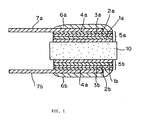
- FIG. 1 is a cross-sectional view of a ceramic electronic component having lead terminals (single sheet ceramic capacitor having lead terminals) according to a preferred embodiment of the present invention.
- a single sheet type ceramic capacitor is described as an example, which has the structure in which lead terminals are bonded to electrodes disposed on both of the front and back surfaces of a sheet ceramic body (ceramic element for a single sheet ceramic capacitor).
- a single sheet ceramic capacitor having lead terminals (hereinafter, referred to as a capacitor briefly) of this preferred embodiment includes a sheet ceramic body 10 made of a dielectric ceramic, electrodes 5a and 5b disposed on both of the front and back surfaces of the ceramic body 10, and lead terminals 7a and 7b bonded to the electrodes 5a and 5b preferably via solder members 6a and 6b.
- the ceramic body 10 is preferably made from a dielectric ceramic such as a BaTiO 3 type, an SrTiO 3 type, a TiO 2 type, or other suitable material.
- the electrodes 5a and 5b to be disposed on both major surfaces of the ceramic body 10 are heated up to a predetermined temperature, by a magnetron sputtering method.
- the temperature at which the ceramic body 10 is heated for sputtering is optional.
- the temperature is set at about 150°C or lower from the standpoint of a reduced residual heat stress in the ceramic body 10.
- the electrodes 5a and 5b include a four-layer structure, that is, first electrode layers 1a and 1b, second electrode layers 2a and 2b, third electrode layers 3a and 3b, and fourth electrode layers 4a and 4b, respectively.
- the first electrode layers 1a and 1b partially constituting the electrodes 5a and 5b are preferably made of an Ni-Ti alloy, respectively, and formed so as to bond closely to both sides (surfaces) of the ceramic body 10.
- the Ni-Ti alloy With respect to the Ni-Ti alloy, an appropriate bonding force can be provided between the Ni-Ti alloy and a ceramic constituting the ceramic body 10.
- the Ni-Ti alloy is an electrode material of which deterioration of the characteristics is minimized when the ceramic is reduced.
- Compositions each having a Ti content (ratio of Ti) in a range of about 5% to about 20% by weight are used as the Ni-Ti alloy. The reason is as follows. If the Ti content of the Ni-Ti alloy is less than about 5% by weight, the bonding force between the alloy and the ceramic is insufficient. That is, a desired bonding strength cannot be obtained. If the Ti content is greater than about 20% by weight, the characteristics of the Ni - Ti alloy are deteriorated due to reduction of the ceramic.
- the second electrode layers 2a and 2b partially constituting the electrodes 5a and 5b are formed on the surface of the first electrode layers 1a and 1b, respectively, and are made of at least one selected from the group consisting of Cu, Ag, and Au.
- the second electrode layers 2a and 2b are provided in order to secure the conductivity.
- the third electrode layers 3a and 3b partially constituting the electrodes 5a and 5b are provided in order to prevent degradation of the conductivity, caused by oxidation of the second electrode layers 2a and 2b, or diffusion of solder components from the solder members 6a and 6b used for bonding of the lead terminals 7a and 7b.
- the third electrode layers 3a and 3b are preferably made of an Ni-Ti alloy. That is, the third electrode layers, preferably made of the Ni-Ti alloy, have a high corrosion resistance, and perform a function of preventing diffusion of Sn and Pb as solder components to protect the second electrode layers 2a and 2b.
- the fourth electrode layers 4a and 4b partially constituting the electrodes 5a and 5b have high wettability for the solders 6a and 6b, and carry out a function of securing soldering-properties of the lead terminals.
- a single sheet ceramic capacitor having lead terminals was prepared by the following method.
- a capacitor (example 1) prepared as described above was left to stand for 1000 hrs while the capacitor was kept at a temperature of about 125°C.
- the electrical characteristics (dielectric constant, dielectric loss, and insulation resistance) of the capacitor taken as a sample were measured.
- TABLE 1 also lists data concerning the wettability of the electrodes and the adhesion force of the electrodes to the ceramic body.
- the electrical characteristics that is, the dielectric constants, the dielectric losses, and the insulation resistances, the wettability of the electrodes for the solders, and the adhesion forces of the electrodes for the ceramic body are comparable to or higher than those of the comparative examples.
- the single sheet type ceramic capacitor having lead terminals is described as an example.
- the present invention is not limited to the single sheet type ceramic capacitor.
- the present invention can be applied to different types of ceramic electronic devices having the structure in which lead terminals are bonded to electrodes bonded on a ceramic element via solder.
- electrode layers of Cu are preferably formed.
- the material for constituting the second and fourth electrode layers is not limited to Cu.
- Various types of combinations including at least one of Cu, Ag, and Au may be used.
- the present invention is not limited to the above-described preferred embodiments.
- the specific shape and size of the ceramic element and the lead terminals, the arrangement patterns of the electrodes, and so forth various applications and modifications can be made without departing from the sprit and the scope of the present invention.
- the electrodes each have the four layer structure including the first electrode made of an Ni-Ti alloy and adapted to be bonded to the surface of the ceramic material constituting the ceramic element, the second electrode layer made of at least one selected from the group consisting of Cu, Ag, and Au and disposed on the first electrode layer, the third electrode layer made of an Ni-Ti alloy and disposed on the second electrode layer, and the fourth electrode layer made of at least one selected from the group consisting of Cu, Ag, and Au and disposed on the third electrode layer, and the lead terminals are bonded to the electrodes having the four layer structure via solder, respectively.
- the lead terminals can be securely bonded to the electrodes, and moreover, deterioration of the characteristics of a product, caused by use in a high temperature environment can be reliably prevented.
- the electrodes each having the four layer structure are preferably formed as follows. (1) as the first electrode layer (undercoat electrode layer), the Ni-Ti alloy having high adhesion to the ceramic is used, (2) the second electrode layer made of Cu or other material suitable for securing the electric conductivity is formed thereon, (3) in addition, the third electrode layer made of an Ni-Ti alloy to suppress a solder component from diffusing is formed thereon, and (4) the fourth electrode layer made of Cu or other material having high soldering properties is formed as the surface layer, and each of the electrode layers performs the functions described above, respectively.
- the bonding strength of the lead terminals is greatly enhanced, and deterioration of the characteristics, caused by use in a high temperature environment is efficiently prevented, so that the reliability is greatly increased.
- the electrodes having high adhesion and soldering properties for the ceramic material constituting the ceramic element can be formed easily and securely by forming the first, second, third, and fourth electrode layers constituting the electrode preferably by a sputtering method, respectively.
- the present invention is highly and practically effective.
- the electrodes having high adhesion and soldering properties for the ceramic material constituting the ceramic element can be formed easily and securely by setting the content of Ti of the Ni-Ti alloy constituting the first and third electrode layers to be in the range of from about 5% to about 20% by weight.
- the present invention is again highly and practically effective.
- the present invention is applied to the single sheet type ceramic capacitor in which the ceramic element is a sheet ceramic body for the single type ceramic capacitor.
- the single sheet ceramic capacitor having lead terminals can be obtained in which adhesion of the ceramic element to the electrodes is very high, the soldering strength of the lead terminals to the electrodes is very high, and moreover, the stability of the characteristics when the capacitor is used in a high temperature environment is excellent.
Landscapes
- Engineering & Computer Science (AREA)
- Power Engineering (AREA)
- Manufacturing & Machinery (AREA)
- Microelectronics & Electronic Packaging (AREA)
- Ceramic Capacitors (AREA)
- Fixed Capacitors And Capacitor Manufacturing Machines (AREA)
- Details Of Resistors (AREA)
Abstract
Description
That is, a desired bonding strength cannot be obtained. If the Ti content is greater than about 20% by weight, the characteristics of the Ni - Ti alloy are deteriorated due to reduction of the ceramic.
The
| Electrode | Electrical characteristics at 125°C after 1000 hrs. | Solder wettability | Adhesion force (N) | ||
| Apparent dielectric constant εr | Dielectric loss (%) | Insulation resistance (MΩ) | |||
| Example 1 | 8250 | 0.35 % | 70000 | good | 37 |
| Comparative Example 1 Cu thick film electrode | 6800 | 0.78 % | 68000 | good | 33 |
| Comparative Example 2 sputtering electrode Cu/Ti/Ni-Cu 300nm/100nm/300nm | 8250 | 0.50 % | 70000 | good | 18 |
| Comparative Example 3 sputtering electrode Cu/Ni-Cu 300nm/300nm | 7200 | 0.78 % | 70000 | good | 13 |
| Ti content (Ti ratio) | |||||
| 5% by | 10% by weight | 15% by weight | 20% by weight | 25% by weight | |
| Dielectric loss (%) | 0.35 | 0.35 | 0.41 | 0.47 | 1.21 |
| Adhesion force (N) | 37 | 38 | 49 | 57 | 57 |
(1) as the first electrode layer (undercoat electrode layer), the Ni-Ti alloy having high adhesion to the ceramic is used, (2) the second electrode layer made of Cu or other material suitable for securing the electric conductivity is formed thereon, (3) in addition, the third electrode layer made of an Ni-Ti alloy to suppress a solder component from diffusing is formed thereon, and (4) the fourth electrode layer made of Cu or other material having high soldering properties is formed as the surface layer, and each of the electrode layers performs the functions described above, respectively. Thus, the bonding strength of the lead terminals is greatly enhanced, and deterioration of the characteristics, caused by use in a high temperature environment is efficiently prevented, so that the reliability is greatly increased.
Claims (18)
- A ceramic electronic component comprising:a ceramic element (10) made of ceramic material;a plurality of electrodes (5a, 5b) disposed on the surface of the ceramic element (10); anda plurality of lead terminals (7a, 7b) attached to the electrodes (5a, 5b); whereinat least one of said electrodes (5a, 5b) has a four layer structure including:(a) a first electrode layer (1a, 1b) made of an Ni-Ti alloy and adapted to adhere to the surface of the ceramic material constituting the ceramic element (10);(b) a second electrode layer (2a, 2b) made of at least one selected from the group consisting of Cu, Ag, and Au and disposed on the first electrode layer (1a, 1b);(c) a third electrode layer (3a, 3b) made of an Ni-Ti alloy and disposed on the second electrode layer (2a, 2b); and(d) a fourth electrode layer (4a, 4b) made of at least one selected from the group consisting of Cu, Ag, and Au and disposed on the third electrode layer (3a, 3b);said lead terminals (7a, 7b) each being bonded to the electrodes (5a, 5b) via solder.
- A ceramic electronic component according to claim 1, wherein the first electrode layer (1a, 1b), the second electrode layer (2a, 2b), the third electrode layer (3a, 3b), and the fourth electrode layer (4a, 4b) constituting the electrode (5a, 5b) are sputtered electrode.
- A ceramic electronic component according to claim 1 or 2, wherein the content of Ti of the Ni-Ti alloy constituting the first (1a, 1b) and third (3a, 3b) electrode layers is in the range of from about 5% to about 20% by weight.
- A ceramic electronic component according to claim 1 or 2, wherein the content of Ti of the Ni-Ti alloy constituting the first (1a, 1b) and third (3a, 3b) electrode layers is in the range of from about 5% to about 10% by weight.
- A ceramic electronic component according to one of the claims 1 to 4, wherein the ceramic element (10) is a sheet ceramic body made of a dielectric ceramic for a single sheet type ceramic capacitor, and the ceramic electronic component is the single sheet type ceramic capacitor.
- A ceramic electronic component according to one of the claims 1 to 5, wherein each of the electrodes (5a, 5b) has the four layer structure.
- A ceramic electronic component according to claim 1, wherein the ceramic element (10) is made of one of BaTiO3, SrTiO3, and TiO2.
- A ceramic electronic component according to one of the claims 1 to 7, wherein the second (2a, 2b) and fourth (4a, 4b) electrode layers are made of Cu.
- A ceramic electronic component according to one of the claims 1 to 7, wherein the second (2a, 2b) and fourth (4a, 4b) electrode layers are made of a combination of Cu, Ag, and Au.
- A method of forming a ceramic electronic component comprising the steps of:providing a ceramic element (10) made of a ceramic material;forming a plurality of electrodes (5a, 5b) on the surface of the ceramic element (10); andforming a plurality of lead terminals (7a, 7b) so as to be attached to the electrodes (5a, 5b); whereinat least one of the plurality of electrodes (7a, 7b) is formed by the following steps:(a) forming a first electrode layer (1a, 1b) on the ceramic element (10), the first electrode being formed of an Ni-Ti alloy and formed to adhere to the surface of the ceramic material constituting the ceramic element (10);(b) forming a second electrode layer (2a, 2b) of at least one selected from the group consisting of Cu, Ag, and Au on the first electrode layer (1a, 1b);(c) forming a third electrode layer (3a, 3b) made of an Ni-Ti alloy on the second electrode layer (2a, 2b); and(d) forming a fourth electrode layer (4a, 4b) of at least one selected from the group consisting of Cu, Ag, and Au on the third electrode layer (3a, 3b); andbonding said lead terminals (7a, 7b) to the electrodes (5a, 5b) via solder.
- A method of forming a ceramic electronic component according to claim 10, wherein the first electrode layer (1a, 1b), the second electrode layer (2a, 2b), the third electrode layer (3a, 3b), and the fourth electrode layer (4a, 4b) constituting the electrode (5a, 5b) are formed via electrode sputtering.
- A method of forming a ceramic electronic component according to claim 10 or 11, wherein the content of Ti of the Ni-Ti alloy constituting the first (1a, 1b) and third (3a, 3b) electrode layers is in the range of from about 5% to about 20% by weight.
- A method of forming a ceramic electronic component according to claim 10 or 11, wherein the content of Ti of the Ni-Ti alloy constituting the first (1a, 1b) and third (3a, 3b) electrode layers is in the range of from about 5% to about 10% by weight.
- A method of forming a ceramic electronic component according to one of the claims 10 to 13, wherein the ceramic element (10) is a sheet ceramic body made of a dielectric ceramic for a single sheet type ceramic capacitor, and the ceramic electronic component is the single sheet type ceramic capacitor.
- A method of forming a ceramic electronic component according to one of the claims 10 to 14, wherein each of the electrodes (5a, 5b) has the four layer structure.
- A method of forming a ceramic electronic component according to claim 10, wherein the ceramic element (10) is formed of one of BaTiO3, SrTiO3, and TiO2.
- A method of forming a ceramic electronic component according to one of the claims 10 to 16, wherein the second (2a, 2b) and fourth (4a, 4b) electrode layers are formed of Cu.
- A method of forming a ceramic electronic component according to one of the claims 10 to 16, wherein the second (2a, 2b) and fourth (4a, 4b) electrode layers are formed of a combination of Cu, Ag, and Au.
Applications Claiming Priority (2)
| Application Number | Priority Date | Filing Date | Title |
|---|---|---|---|
| JP2000070002A JP3446713B2 (en) | 2000-03-14 | 2000-03-14 | Ceramic electronic components with lead terminals |
| JP2000070002 | 2000-03-14 |
Publications (3)
| Publication Number | Publication Date |
|---|---|
| EP1134757A2 true EP1134757A2 (en) | 2001-09-19 |
| EP1134757A3 EP1134757A3 (en) | 2004-01-21 |
| EP1134757B1 EP1134757B1 (en) | 2004-11-24 |
Family
ID=18588795
Family Applications (1)
| Application Number | Title | Priority Date | Filing Date |
|---|---|---|---|
| EP01105906A Expired - Lifetime EP1134757B1 (en) | 2000-03-14 | 2001-03-09 | Ceramic electronic component having lead terminal |
Country Status (6)
| Country | Link |
|---|---|
| US (1) | US6373684B2 (en) |
| EP (1) | EP1134757B1 (en) |
| JP (1) | JP3446713B2 (en) |
| KR (1) | KR100371574B1 (en) |
| CN (1) | CN1192402C (en) |
| DE (1) | DE60107311T2 (en) |
Cited By (1)
| Publication number | Priority date | Publication date | Assignee | Title |
|---|---|---|---|---|
| EP1622216A1 (en) * | 2004-06-30 | 2006-02-01 | Kabushiki Kaisha Kobe Seiko Sho | Titanium material and method for manufacturing the same |
Families Citing this family (11)
| Publication number | Priority date | Publication date | Assignee | Title |
|---|---|---|---|---|
| US6498561B2 (en) * | 2001-01-26 | 2002-12-24 | Cornerstone Sensors, Inc. | Thermistor and method of manufacture |
| TW200412603A (en) * | 2003-10-02 | 2004-07-16 | wei-hao Zhang | Electrode layer manufacturing method to inhibit the corona effect of ceramic capacitor body |
| US7119655B2 (en) * | 2004-11-29 | 2006-10-10 | Therm-O-Disc, Incorporated | PTC circuit protector having parallel areas of effective resistance |
| US20090140423A1 (en) * | 2007-11-29 | 2009-06-04 | International Business Machines Corporation | Underbump metallurgy employing sputter-deposited nickel titanium alloy |
| KR101018645B1 (en) * | 2008-11-03 | 2011-03-03 | 삼화콘덴서공업주식회사 | High Voltage and High Frequency Ceramic Capacitors |
| JP2010129621A (en) * | 2008-11-26 | 2010-06-10 | Murata Mfg Co Ltd | Laminated ceramic electronic component and manufacturing method of the same |
| CN102800475B (en) * | 2012-08-03 | 2015-12-09 | 广东风华高新科技股份有限公司 | Vacuum sputtering multilayer metallic electrode disk ceramic capacitor and preparation method thereof |
| KR101656723B1 (en) * | 2015-06-30 | 2016-09-12 | 재단법인 오송첨단의료산업진흥재단 | Feedthrough making method |
| CN105355348A (en) * | 2015-11-30 | 2016-02-24 | 兴勤(常州)电子有限公司 | Electronic component multi-layer composite metal electrode and making process thereof |
| CN107331489A (en) * | 2017-05-16 | 2017-11-07 | 揭阳空港经济区弘新电子有限公司 | A kind of manufacturing process of combination electrode electronic ceramic component |
| KR102742471B1 (en) * | 2024-05-14 | 2024-12-16 | 주식회사 에스엠티 | Heater Power Supply Unit for Semiconductor CVD Process |
Family Cites Families (6)
| Publication number | Priority date | Publication date | Assignee | Title |
|---|---|---|---|---|
| US3581167A (en) * | 1970-02-19 | 1971-05-25 | Erie Technological Prod Inc | Reinforced ceramic capacitor and method of making the same |
| DE3638286A1 (en) * | 1986-11-10 | 1988-05-11 | Siemens Ag | Electrical component, made of ceramic and having multilayer metallisation, and a method for its production |
| JP2803227B2 (en) * | 1989-09-29 | 1998-09-24 | 株式会社村田製作所 | Multilayer electronic components |
| EP0514149B1 (en) * | 1991-05-16 | 1995-09-27 | Nec Corporation | Thin film capacitor |
| JP3031268B2 (en) * | 1996-11-20 | 2000-04-10 | 株式会社村田製作所 | Porcelain capacitors |
| JP3468122B2 (en) * | 1998-09-17 | 2003-11-17 | 住友金属鉱山株式会社 | TiNi-based target material and electrode material |
-
2000
- 2000-03-14 JP JP2000070002A patent/JP3446713B2/en not_active Expired - Lifetime
-
2001
- 2001-02-07 CN CNB011026596A patent/CN1192402C/en not_active Expired - Lifetime
- 2001-02-16 US US09/784,844 patent/US6373684B2/en not_active Expired - Lifetime
- 2001-03-08 KR KR10-2001-0011997A patent/KR100371574B1/en not_active Expired - Lifetime
- 2001-03-09 EP EP01105906A patent/EP1134757B1/en not_active Expired - Lifetime
- 2001-03-09 DE DE60107311T patent/DE60107311T2/en not_active Expired - Lifetime
Cited By (1)
| Publication number | Priority date | Publication date | Assignee | Title |
|---|---|---|---|---|
| EP1622216A1 (en) * | 2004-06-30 | 2006-02-01 | Kabushiki Kaisha Kobe Seiko Sho | Titanium material and method for manufacturing the same |
Also Published As
| Publication number | Publication date |
|---|---|
| CN1192402C (en) | 2005-03-09 |
| US6373684B2 (en) | 2002-04-16 |
| KR100371574B1 (en) | 2003-02-07 |
| EP1134757B1 (en) | 2004-11-24 |
| JP3446713B2 (en) | 2003-09-16 |
| KR20010091933A (en) | 2001-10-23 |
| DE60107311T2 (en) | 2005-11-24 |
| US20010048580A1 (en) | 2001-12-06 |
| JP2001267174A (en) | 2001-09-28 |
| CN1313616A (en) | 2001-09-19 |
| EP1134757A3 (en) | 2004-01-21 |
| DE60107311D1 (en) | 2004-12-30 |
Similar Documents
| Publication | Publication Date | Title |
|---|---|---|
| JP3031268B2 (en) | Porcelain capacitors | |
| JP3376970B2 (en) | Ceramic electronic components | |
| JP4423707B2 (en) | Manufacturing method of multilayer ceramic electronic component | |
| KR100908985B1 (en) | Ceramic Electronic Components and Manufacturing Method Thereof | |
| JP2017191929A (en) | Multilayer capacitor and manufacturing method thereof | |
| US11682526B2 (en) | Multilayer ceramic electronic component and board for mounting of the same | |
| JP2001307947A (en) | Laminated chip component and its manufacturing method | |
| EP1134757B1 (en) | Ceramic electronic component having lead terminal | |
| JP3494431B2 (en) | Manufacturing method of ceramic electronic component and ceramic electronic component | |
| KR102946062B1 (en) | Multilayer elcetronic component | |
| JP2002203737A (en) | Laminated ceramic electronic parts and its manufacturing method | |
| US11551872B2 (en) | Multilayer ceramic capacitor | |
| JP2001237137A (en) | Multilayer capacitor and external electrode conductor paste therefor | |
| JP3436127B2 (en) | Terminal electrodes for electronic components and electronic components | |
| JPH10163067A (en) | External electrodes for chip-type electronic components | |
| JPH08203769A (en) | Ceramic electronic component | |
| JP3458701B2 (en) | Electronic component and method of manufacturing the same | |
| JPH09115772A (en) | External electrodes for chip-type electronic components | |
| JP2002252124A (en) | Chip-type electronic component and method of manufacturing the same | |
| JP2002198253A (en) | Ceramic electronic components and conductive paste | |
| JP4556337B2 (en) | Manufacturing method of multilayer ceramic electronic component | |
| US20240249885A1 (en) | Multilayer ceramic electronic component | |
| JP2006332284A (en) | Electronic component and method for manufacturing electronic component | |
| JP3556377B2 (en) | Wiring board | |
| JP2773314B2 (en) | Multilayer ceramic capacitors |
Legal Events
| Date | Code | Title | Description |
|---|---|---|---|
| PUAI | Public reference made under article 153(3) epc to a published international application that has entered the european phase |
Free format text: ORIGINAL CODE: 0009012 |
|
| 17P | Request for examination filed |
Effective date: 20010309 |
|
| AK | Designated contracting states |
Kind code of ref document: A2 Designated state(s): AT BE CH CY DE DK ES FI FR GB GR IE IT LI LU MC NL PT SE TR |
|
| AX | Request for extension of the european patent |
Free format text: AL;LT;LV;MK;RO;SI |
|
| PUAL | Search report despatched |
Free format text: ORIGINAL CODE: 0009013 |
|
| AK | Designated contracting states |
Kind code of ref document: A3 Designated state(s): AT BE CH CY DE DK ES FI FR GB GR IE IT LI LU MC NL PT SE TR |
|
| AX | Request for extension of the european patent |
Extension state: AL LT LV MK RO SI |
|
| RIC1 | Information provided on ipc code assigned before grant |
Ipc: 7H 01L 41/047 B Ipc: 7H 01C 1/142 B Ipc: 7H 01G 4/252 A Ipc: 7H 01G 1/14 B Ipc: 7H 01G 4/12 B |
|
| GRAP | Despatch of communication of intention to grant a patent |
Free format text: ORIGINAL CODE: EPIDOSNIGR1 |
|
| RIC1 | Information provided on ipc code assigned before grant |
Ipc: 7H 01G 4/252 A |
|
| GRAS | Grant fee paid |
Free format text: ORIGINAL CODE: EPIDOSNIGR3 |
|
| GRAA | (expected) grant |
Free format text: ORIGINAL CODE: 0009210 |
|
| AKX | Designation fees paid |
Designated state(s): DE FR GB |
|
| AK | Designated contracting states |
Kind code of ref document: B1 Designated state(s): DE FR GB |
|
| PG25 | Lapsed in a contracting state [announced via postgrant information from national office to epo] |
Ref country code: FR Free format text: LAPSE BECAUSE OF FAILURE TO SUBMIT A TRANSLATION OF THE DESCRIPTION OR TO PAY THE FEE WITHIN THE PRESCRIBED TIME-LIMIT Effective date: 20041124 |
|
| REG | Reference to a national code |
Ref country code: GB Ref legal event code: FG4D |
|
| REF | Corresponds to: |
Ref document number: 60107311 Country of ref document: DE Date of ref document: 20041230 Kind code of ref document: P |
|
| REG | Reference to a national code |
Ref country code: IE Ref legal event code: FG4D |
|
| PG25 | Lapsed in a contracting state [announced via postgrant information from national office to epo] |
Ref country code: GB Free format text: LAPSE BECAUSE OF NON-PAYMENT OF DUE FEES Effective date: 20050309 |
|
| PLBE | No opposition filed within time limit |
Free format text: ORIGINAL CODE: 0009261 |
|
| STAA | Information on the status of an ep patent application or granted ep patent |
Free format text: STATUS: NO OPPOSITION FILED WITHIN TIME LIMIT |
|
| 26N | No opposition filed |
Effective date: 20050825 |
|
| GBPC | Gb: european patent ceased through non-payment of renewal fee |
Effective date: 20050309 |
|
| EN | Fr: translation not filed | ||
| PGFP | Annual fee paid to national office [announced via postgrant information from national office to epo] |
Ref country code: DE Payment date: 20200320 Year of fee payment: 20 |
|
| REG | Reference to a national code |
Ref country code: DE Ref legal event code: R071 Ref document number: 60107311 Country of ref document: DE |