EP1130722A2 - Semiconductor laser device - Google Patents
Semiconductor laser device Download PDFInfo
- Publication number
- EP1130722A2 EP1130722A2 EP00311645A EP00311645A EP1130722A2 EP 1130722 A2 EP1130722 A2 EP 1130722A2 EP 00311645 A EP00311645 A EP 00311645A EP 00311645 A EP00311645 A EP 00311645A EP 1130722 A2 EP1130722 A2 EP 1130722A2
- Authority
- EP
- European Patent Office
- Prior art keywords
- layer
- semiconductor laser
- laser device
- depletion enhancement
- current blocking
- Prior art date
- Legal status (The legal status is an assumption and is not a legal conclusion. Google has not performed a legal analysis and makes no representation as to the accuracy of the status listed.)
- Granted
Links
Images











Classifications
-
- H—ELECTRICITY
- H01—ELECTRIC ELEMENTS
- H01S—DEVICES USING THE PROCESS OF LIGHT AMPLIFICATION BY STIMULATED EMISSION OF RADIATION [LASER] TO AMPLIFY OR GENERATE LIGHT; DEVICES USING STIMULATED EMISSION OF ELECTROMAGNETIC RADIATION IN WAVE RANGES OTHER THAN OPTICAL
- H01S5/00—Semiconductor lasers
- H01S5/30—Structure or shape of the active region; Materials used for the active region
-
- H—ELECTRICITY
- H01—ELECTRIC ELEMENTS
- H01S—DEVICES USING THE PROCESS OF LIGHT AMPLIFICATION BY STIMULATED EMISSION OF RADIATION [LASER] TO AMPLIFY OR GENERATE LIGHT; DEVICES USING STIMULATED EMISSION OF ELECTROMAGNETIC RADIATION IN WAVE RANGES OTHER THAN OPTICAL
- H01S5/00—Semiconductor lasers
- H01S5/20—Structure or shape of the semiconductor body to guide the optical wave ; Confining structures perpendicular to the optical axis, e.g. index or gain guiding, stripe geometry, broad area lasers, gain tailoring, transverse or lateral reflectors, special cladding structures, MQW barrier reflection layers
- H01S5/22—Structure or shape of the semiconductor body to guide the optical wave ; Confining structures perpendicular to the optical axis, e.g. index or gain guiding, stripe geometry, broad area lasers, gain tailoring, transverse or lateral reflectors, special cladding structures, MQW barrier reflection layers having a ridge or stripe structure
- H01S5/223—Buried stripe structure
- H01S5/2231—Buried stripe structure with inner confining structure only between the active layer and the upper electrode
-
- H—ELECTRICITY
- H01—ELECTRIC ELEMENTS
- H01S—DEVICES USING THE PROCESS OF LIGHT AMPLIFICATION BY STIMULATED EMISSION OF RADIATION [LASER] TO AMPLIFY OR GENERATE LIGHT; DEVICES USING STIMULATED EMISSION OF ELECTROMAGNETIC RADIATION IN WAVE RANGES OTHER THAN OPTICAL
- H01S5/00—Semiconductor lasers
- H01S5/06—Arrangements for controlling the laser output parameters, e.g. by operating on the active medium
- H01S5/062—Arrangements for controlling the laser output parameters, e.g. by operating on the active medium by varying the potential of the electrodes
- H01S5/06226—Modulation at ultra-high frequencies
-
- H—ELECTRICITY
- H01—ELECTRIC ELEMENTS
- H01S—DEVICES USING THE PROCESS OF LIGHT AMPLIFICATION BY STIMULATED EMISSION OF RADIATION [LASER] TO AMPLIFY OR GENERATE LIGHT; DEVICES USING STIMULATED EMISSION OF ELECTROMAGNETIC RADIATION IN WAVE RANGES OTHER THAN OPTICAL
- H01S5/00—Semiconductor lasers
- H01S5/20—Structure or shape of the semiconductor body to guide the optical wave ; Confining structures perpendicular to the optical axis, e.g. index or gain guiding, stripe geometry, broad area lasers, gain tailoring, transverse or lateral reflectors, special cladding structures, MQW barrier reflection layers
- H01S5/22—Structure or shape of the semiconductor body to guide the optical wave ; Confining structures perpendicular to the optical axis, e.g. index or gain guiding, stripe geometry, broad area lasers, gain tailoring, transverse or lateral reflectors, special cladding structures, MQW barrier reflection layers having a ridge or stripe structure
- H01S5/2205—Structure or shape of the semiconductor body to guide the optical wave ; Confining structures perpendicular to the optical axis, e.g. index or gain guiding, stripe geometry, broad area lasers, gain tailoring, transverse or lateral reflectors, special cladding structures, MQW barrier reflection layers having a ridge or stripe structure comprising special burying or current confinement layers
- H01S5/2206—Structure or shape of the semiconductor body to guide the optical wave ; Confining structures perpendicular to the optical axis, e.g. index or gain guiding, stripe geometry, broad area lasers, gain tailoring, transverse or lateral reflectors, special cladding structures, MQW barrier reflection layers having a ridge or stripe structure comprising special burying or current confinement layers based on III-V materials
-
- H—ELECTRICITY
- H01—ELECTRIC ELEMENTS
- H01S—DEVICES USING THE PROCESS OF LIGHT AMPLIFICATION BY STIMULATED EMISSION OF RADIATION [LASER] TO AMPLIFY OR GENERATE LIGHT; DEVICES USING STIMULATED EMISSION OF ELECTROMAGNETIC RADIATION IN WAVE RANGES OTHER THAN OPTICAL
- H01S5/00—Semiconductor lasers
- H01S5/20—Structure or shape of the semiconductor body to guide the optical wave ; Confining structures perpendicular to the optical axis, e.g. index or gain guiding, stripe geometry, broad area lasers, gain tailoring, transverse or lateral reflectors, special cladding structures, MQW barrier reflection layers
- H01S5/22—Structure or shape of the semiconductor body to guide the optical wave ; Confining structures perpendicular to the optical axis, e.g. index or gain guiding, stripe geometry, broad area lasers, gain tailoring, transverse or lateral reflectors, special cladding structures, MQW barrier reflection layers having a ridge or stripe structure
- H01S5/2205—Structure or shape of the semiconductor body to guide the optical wave ; Confining structures perpendicular to the optical axis, e.g. index or gain guiding, stripe geometry, broad area lasers, gain tailoring, transverse or lateral reflectors, special cladding structures, MQW barrier reflection layers having a ridge or stripe structure comprising special burying or current confinement layers
- H01S5/2222—Structure or shape of the semiconductor body to guide the optical wave ; Confining structures perpendicular to the optical axis, e.g. index or gain guiding, stripe geometry, broad area lasers, gain tailoring, transverse or lateral reflectors, special cladding structures, MQW barrier reflection layers having a ridge or stripe structure comprising special burying or current confinement layers having special electric properties
-
- H—ELECTRICITY
- H01—ELECTRIC ELEMENTS
- H01S—DEVICES USING THE PROCESS OF LIGHT AMPLIFICATION BY STIMULATED EMISSION OF RADIATION [LASER] TO AMPLIFY OR GENERATE LIGHT; DEVICES USING STIMULATED EMISSION OF ELECTROMAGNETIC RADIATION IN WAVE RANGES OTHER THAN OPTICAL
- H01S5/00—Semiconductor lasers
- H01S5/20—Structure or shape of the semiconductor body to guide the optical wave ; Confining structures perpendicular to the optical axis, e.g. index or gain guiding, stripe geometry, broad area lasers, gain tailoring, transverse or lateral reflectors, special cladding structures, MQW barrier reflection layers
- H01S5/22—Structure or shape of the semiconductor body to guide the optical wave ; Confining structures perpendicular to the optical axis, e.g. index or gain guiding, stripe geometry, broad area lasers, gain tailoring, transverse or lateral reflectors, special cladding structures, MQW barrier reflection layers having a ridge or stripe structure
- H01S5/2205—Structure or shape of the semiconductor body to guide the optical wave ; Confining structures perpendicular to the optical axis, e.g. index or gain guiding, stripe geometry, broad area lasers, gain tailoring, transverse or lateral reflectors, special cladding structures, MQW barrier reflection layers having a ridge or stripe structure comprising special burying or current confinement layers
- H01S5/2222—Structure or shape of the semiconductor body to guide the optical wave ; Confining structures perpendicular to the optical axis, e.g. index or gain guiding, stripe geometry, broad area lasers, gain tailoring, transverse or lateral reflectors, special cladding structures, MQW barrier reflection layers having a ridge or stripe structure comprising special burying or current confinement layers having special electric properties
- H01S5/2226—Structure or shape of the semiconductor body to guide the optical wave ; Confining structures perpendicular to the optical axis, e.g. index or gain guiding, stripe geometry, broad area lasers, gain tailoring, transverse or lateral reflectors, special cladding structures, MQW barrier reflection layers having a ridge or stripe structure comprising special burying or current confinement layers having special electric properties semiconductors with a specific doping
-
- H—ELECTRICITY
- H01—ELECTRIC ELEMENTS
- H01S—DEVICES USING THE PROCESS OF LIGHT AMPLIFICATION BY STIMULATED EMISSION OF RADIATION [LASER] TO AMPLIFY OR GENERATE LIGHT; DEVICES USING STIMULATED EMISSION OF ELECTROMAGNETIC RADIATION IN WAVE RANGES OTHER THAN OPTICAL
- H01S5/00—Semiconductor lasers
- H01S5/20—Structure or shape of the semiconductor body to guide the optical wave ; Confining structures perpendicular to the optical axis, e.g. index or gain guiding, stripe geometry, broad area lasers, gain tailoring, transverse or lateral reflectors, special cladding structures, MQW barrier reflection layers
- H01S5/22—Structure or shape of the semiconductor body to guide the optical wave ; Confining structures perpendicular to the optical axis, e.g. index or gain guiding, stripe geometry, broad area lasers, gain tailoring, transverse or lateral reflectors, special cladding structures, MQW barrier reflection layers having a ridge or stripe structure
- H01S5/2205—Structure or shape of the semiconductor body to guide the optical wave ; Confining structures perpendicular to the optical axis, e.g. index or gain guiding, stripe geometry, broad area lasers, gain tailoring, transverse or lateral reflectors, special cladding structures, MQW barrier reflection layers having a ridge or stripe structure comprising special burying or current confinement layers
- H01S5/2222—Structure or shape of the semiconductor body to guide the optical wave ; Confining structures perpendicular to the optical axis, e.g. index or gain guiding, stripe geometry, broad area lasers, gain tailoring, transverse or lateral reflectors, special cladding structures, MQW barrier reflection layers having a ridge or stripe structure comprising special burying or current confinement layers having special electric properties
- H01S5/2227—Structure or shape of the semiconductor body to guide the optical wave ; Confining structures perpendicular to the optical axis, e.g. index or gain guiding, stripe geometry, broad area lasers, gain tailoring, transverse or lateral reflectors, special cladding structures, MQW barrier reflection layers having a ridge or stripe structure comprising special burying or current confinement layers having special electric properties special thin layer sequence
Definitions
- the present invention relates to a semiconductor laser device having a current blocking layer.
- FIG. 34 is a typical sectional view showing a conventional semiconductor laser device 120 described in Japanese Patent Laying-Open No. 8-222801 (1996).
- an n-type cladding layer 122, an active layer 123, a p-type cladding layer 124 and a p-type contact layer 127 are successively formed on an n-type substrate 121, and the p-type contact layer 127 and the p-type cladding layer 124 are etched for forming flat portions on a ridge portion and on both sides of the ridge portion.
- a first current blocking layer 125 having a low carrier concentration is formed on the flat portions of the p-type cladding layer 124 located on both sides of the ridge portion, and an n-type current blocking layer 126 is formed on the first current blocking layer 125 having a low carrier concentration.
- a p-type contact layer 128 is formed on the p-type contact layer 127 and the n-type current blocking layer 126.
- n-type current blocking layer 126 cuts off a current so that the current is injected into the ridge portion in a narrowed state.
- a p-n junction formed between an n-type current blocking layer and a p-type cladding layer has large electric capacitance, and hence serves as a factor inhibiting high-speed operation of a semiconductor laser device.
- the electric capacitance of the p-n junction is increased as the carrier concentration in this p-n junction is increased.
- the semiconductor laser device 120 shown in Fig .34 is provided with the current blocking layer 125 having a low carrier concentration, in order to reduce the electric capacitance in the p-n junction between the n-type current blocking layer 126 and the p-type cladding layer 124.
- This current blocking layer 125 has a lower carrier concentration than the n-type current blocking layer 126. Therefore, the current blocking layer 125 having a low carrier concentration defines a depletion region in the p-n junction between the n-type current blocking layer 126 and the p-type cladding layer 124, for reducing the electric capacitance.
- the semiconductor laser device 120 is enabled to operate at a high frequency.
- valence bands of the p-type cladding layer 124 and the current blocking layer 125 of a low carrier concentration have energy band structures shown in Fig. 35.
- Fig. 35 is a model diagram showing the energy band structures of the valence bands of the p-type cladding layer 124 and the current blocking layer 125 having a low carrier concentration.
- the band gap of the current blocking layer 125 having a low carrier concentration is sufficiently smaller than the band gap of the p-type cladding layer 124, and hence carriers are readily injected from the p-type cladding layer 124 into the current blocking layer 125 having a low carrier concentration and stored therein.
- An object of the present invention is to provide a semiconductor laser device sufficiently increased in operating speed.
- a semiconductor laser device comprises an active layer, a first cladding layer of a first conduction type provided on the active layer, a current blocking layer of a second conduction type provided on the first cladding layer except a current injection region, a low carrier concentration layer provided on the side of the current blocking layer between the first cladding layer and the current blocking layer and having a lower carrier concentration than the current blocking layer and a depletion enhancement layer provided on the side of the first cladding layer between the first cladding layer and the current blocking layer for inhibiting storage of carriers in the low carrier concentration layer.
- the depletion enhancement layer inhibits storage of carriers from the first cladding layer into the low carrier concentration layer.
- the low carrier concentration layer is kept in a depleted state. Therefore, electric capacitance between the current blocking layer and the first cladding layer is kept small for sufficiently increasing the operating speed of the semiconductor laser device.
- the band gaps of the first cladding layer, the depletion enhancement layer and the low carrier concentration layer may be reduced in this order.
- the depletion enhancement layer having an intermediate band gap is provided between the first cladding layer having a large band gap and the low carrier concentration layer having a small band gap.
- the band offset between the first cladding layer and the depletion enhancement layer is smaller than the band offset between the first cladding layer and the low carrier concentration layer, whereby carriers are hardly injected from the first cladding layer into the depletion enhancement layer while carriers are more hardly injected into the low carrier concentration layer. Further, the carriers are injected from the first cladding layer into both of the low carrier concentration layer and the depletion enhancement layer in a divided manner, whereby the quantity of carriers stored in the low carrier concentration layer is reduced.
- storage of carriers in the low carrier concentration layer can be inhibited by the simple structure of setting the band gap of the depletion enhancement layer to the intermediate level between the low carrier concentration layer and the first cladding layer.
- the first cladding layer may have a flat portion formed on the active layer and a ridge portion formed on the flat portion in the current injection region, the depletion enhancement layer may be formed on the flat portion located on both sides of the ridge portion and on the side surfaces of the ridge portion, and the low carrier concentration layer and the current blocking layer may be successively formed on the depletion enhancement layer.
- the depletion enhancement layer inhibits storage of carriers from the flat portion of the first cladding layer into the low carrier concentration layer.
- the low carrier concentration layer is kept in the depleted state, and the electric capacitance between the flat portion of the first cladding layer and the current blocking layer is kept small.
- the thickness of the depletion enhancement layer is preferably at least 10 nm.
- the semiconductor laser device is more improved in high-frequency characteristic.
- the thickness of the depletion enhancement layer is preferably at least 15 nm.
- the semiconductor laser device is further improved in high-frequency characteristic.
- the semiconductor laser device may further comprise a ridge-shaped second cladding layer of a first conduction type provided on the depletion enhancement layer in the current injection region, the depletion enhancement layer may be formed on the first cladding layer, and the lower carrier concentration layer and the current blocking layer may be successively formed on the depletion enhancement layer located on both sides of the second cladding layer and on the side surfaces of the second cladding layer.
- the depletion enhancement layer inhibits storage of carriers from the first cladding layer into the low carrier concentration layer.
- the low carrier concentration layer is kept in the depleted state and the electric capacitance between the first cladding layer and the current blocking layer is kept small.
- the thickness of the depletion enhancement layer is preferably at least 15 nm.
- the semiconductor laser device is more improved in high-frequency characteristic.
- the thickness of the depletion enhancement layer is preferably at least 20 nm.
- the semiconductor laser device is further improved in high-frequency characteristic.
- the depletion enhancement layer, the low carrier concentration layer and the current blocking layer may be successively formed on the first cladding layer except the current injection region, and the semiconductor laser device may further comprise a second cladding layer of a first conduction type provided to fill up a space enclosed with the side surfaces of the depletion enhancement layer, the low carrier concentration layer and the current blocking layer and the upper surface of the first cladding layer in the current injection region.
- the depletion enhancement layer inhibits storage of carriers from the first cladding layer into the low carrier concentration layer.
- the low carrier concentration layer is kept in the depleted state and the electric capacitance between the first cladding layer and the current blocking layer is kept small.
- the thickness of the depletion enhancement layer is preferably at least 15 nm.
- the semiconductor laser device is more improved in high-frequency characteristic.
- the thickness of the depletion enhancement layer is preferably at least 20 nm.
- the semiconductor laser device is further improved in high-frequency characteristic.
- the depletion enhancement layer may have a single-layer structure or a superlattice structure.
- the active layer may include a layer made of (Al x1 Ga 1- x1 )y1In 1-y1 P
- the depletion enhancement layer may be made of (Al x2 Ga 1-x2 ) y2 In 1-y2 P or Al x2 Ga 1-x2 As
- the low carrier concentration layer may be made of (Al x3 Ga 1-x3 ) y3 In 1-y3 P or Al x3 Ga 1-x3 As
- the current blocking layer may be made of (Al x4 Ga 1-x4 ) y4 In 1-y4 P or Al x4 Ga 1-x4 As
- x1, x2, x3, x4, y1, y2, y3 and y4 may be at least zero and not more than 1 respectively.
- the active layer may include a layer made of Al x1 Ga 1-x1 As, the depletion enhancement layer may be made of Al x2 Ga 1-x2 As, the low carrier concentration layer may be made of Al x3 Ga 1-x3 As, the current blocking layer may be made of Al x4 Ga 1-x4 As , and x1, x2, x3 and x4 may be at least zero and not more than 1 respectively.
- the active layer may be made of In x1 Ga 1-x1 N
- the depletion enhancement layer may be made of Al x2 Ga 1-x2 N
- the low carrier concentration layer may be made of Al x3 Ga 1-x3 N
- the current blocking layer may be made of Al x4 Ga 1-x4 N
- x1, x2, x3 and x4 may be at least zero and not more than 1 respectively.
- the active layer preferably includes a layer made of (Al x1 Ga 1-x1 ) y1 In 1-y1 P, the depletion enhancement layer is preferably made of (Al x2 Ga 1-x2 ) y2 In 1-y2 P, the low carrier concentration layer is preferably made of Al x3 Ga 1-x3 As, the current blocking layer is preferably made of Al x4 Ga 1-x4 As, x1, x2, x3, x4, y1 and y2 are preferably at least zero and not more than 1 respectively, and the first conduction type is preferably the p type, and the second conduction type is preferably the n type.
- a semiconductor laser device comprises an active layer, a first claddinglayer of a first conduction type provided on the active layer, a first current blocking layer having a low carrier concentration provided on the first cladding layer except a current injection region and a depletion enhancement layer formed between the first cladding layer and the first current blocking layer for inhibiting storage of carriers in the first current blocking layer, while the depletion enhancement layer has an energy level in band gap supplying second conduction type carriers to compensate for first conduction type carriers supplied from the first cladding layer due to a modulation doping effect.
- the first current blocking layer having a low carrier concentration is an undoped layer or a layer doped with a low density of impurity in a range capable of blocking a current.
- the depletion enhancement layer formed with the energy level in band gap supplying the second conduction type carriers is formed between the first cladding layer and the first current blocking layer.
- the second conduction type carriers supplied from the energy level in band gap of the depletion enhancement layer compensate for the first conduction type carriers supplied from the first cladding layer. Therefore, storage of carriers can be prevented in the first current blocking layer having a low carrier concentration. Thus, the first current blocking layer is kept in a depleted state. Therefore, electric capacitance generated between the first current blocking layer and the first cladding layer can be reduced and the operating speed of the semiconductor laser device can be sufficiently increased.
- the first current blocking layer has a narrower band gap than the first cladding layer.
- the first current blocking layer has a narrower band gap than the first cladding layer, carriers are readily injected from the first cladding layer into the first current blocking layer and stored therein.
- the depletion enhancement layer formed between the first cladding layer and the first current blocking layer can inhibit storage of carriers in the first current blocking layer.
- the energy level in band gap preferably has such density that substantially all energy level in band gap ionize under a condition applying no bias voltage voltage. In this case, it is possible to effectively compensate for the first conduction type carriers supplied from the first cladding layer. Therefore, storage of carriers in the first current blocking layer having a low carrier concentration can be more effectively inhibited.
- the energy level in band gap may be formed by doping with a second conduction type impurity.
- the depletion enhancement layer provided with the energy level in band gap can be readily formed.
- the material of the depletion enhancement layer may be the same as the material of the first current blocking layer. In this case, the band gap width of the depletion enhancement layer and the first current blocking layer are equalized with each other.
- the first cladding layer may have a larger band gap than the depletion enhancement layer
- the semiconductor laser device may further comprise an intermediate band gap layer provided between the first cladding layer and the depletion enhancement layer and having a band gap smaller than the band gap of the first cladding layer and larger than the band gap of the depletion enhancement layer.
- carriers are hardly injected from the first cladding layer into the depletion enhancement layer and hardly injected into the first current blocking layer having a low carrier concentration either due to the intermediate band gap layer provided between the first cladding layer and the depletion enhancement layer.
- the carriers are injected into both of the depletion enhancement layer and the intermediate band gap layer in a divided manner, and hence hardly injected into the first current blocking layer.
- the ranges of the thickness and the carrier concentration of the depletion enhancement layer capable increasing the operating speed of the semiconductor layer device are widened by providing the intermediate band gap layer in the aforementioned manner. Therefore, the thickness and the carrier concentration of the depletion enhancement layer can be readily set so that the depletion enhancement layer can be readily prepared.
- the depletion enhancement layer may have a band gap smaller than the band gap of the first cladding layer and larger than the band gap of the first current blocking layer.
- the depletion enhancement layer serves as the aforementioned intermediate band gap layer, thereby further inhibiting storage of carriers in the first current blocking layer.
- the ranges of the thickness and the carrier concentration of the depletion enhancement layer capable of increasing the operating speed of the semiconductor laser device are widened.
- the thickness and the carrier concentration of the depletion enhancement layer can be readily set so that the depletion enhancement layer can be readily prepared.
- the first cladding layer may have a flat portion formed on the active layer and a ridge portion formed on the flat portion in the current injection region, the depletion enhancement layer may be formed on the flat portion located on both sides of the ridge portion and on the side surfaces of the ridge portion, and the first current blocking layer may be formed on the depletion enhancement layer.
- a ridge guided semiconductor laser device improved in-operating speed is implemented.
- the depletion enhancement layer and the first current blocking layer may be successively formed on the first cladding layer except the current injection region, and the semiconductor laser device may further comprise a second cladding layer of a first conduction type provided to fill up a space enclosed with the side surfaces of the depletion enhancement layer and the first current blocking layer and the upper surface of the first cladding layer in the current injection region.
- a self-aligned semiconductor laser device improved in operating speed is implemented.
- the depletion enhancement layer may be formed on a region excluding the current injection region. In this case, a current is quickly injected into the current injection region provided with no depletion enhancement layer of the opposite conduction type.
- the semiconductor laser device may further comprise a second current blocking layer of a second conduction type provided on the first current blocking layer.
- a semiconductor laser device comprises an active layer, a first cladding layer of a first conduction type provided on the active layer, a first current blocking layer having a low carrier concentration provided on the first cladding layer except a current injection region and a depletion enhancement layer formed between the first cladding layer and the first current blocking layer for inhibiting storage of carriers in the first current blocking layer.
- the depletion enhancement layer inhibits storage of carriers from the first cladding layer into the first current blocking layer having a low carrier concentration.
- the first current blocking layer having a low carrier concentration is kept in a depleted state. Therefore, electric capacitance between the first current blocking layer having a low carrier concentration and the first cladding layer is kept small for sufficiently increasing the operating speed of the semiconductor laser device.
- the first current blocking layer having a low concentration has a narrower band gap than the first cladding layer.
- the first current blocking layer having a low carrier concentration has a narrower band gap than the first cladding layer, carriers are readily injected from the first cladding layer into the first current blocking layer having a low carrier concentration and stored therein.
- the depletion enhancement layer formed between the first cladding layer and the first current blocking layer having a low carrier concentration can inhibit storage of carriers in the first current blocking layer having a low carrier concentration.
- the band gaps of the first cladding layer, the depletion enhancement layer and the first current blocking layer having a low carrier concentration may be reduced in this order.
- the depletion enhancement layer having an intermediate band gap is provided between the first cladding layer having a large band gap and the first current blocking layer having a low carrier concentration having a small band gap.
- the band offset between the first cladding layer and the depletion enhancement layer is smaller than the band offset between the first cladding layer and the first current blocking layer having a low carrier concentration, whereby carriers are hardly injected from the first cladding layer into the depletion enhancement layer while carriers are more hardly injected into the first current blocking layer having a low carrier concentration. Further, the carriers are injected from the first cladding layer into both of the first current blocking layer having a low carrier concentration and the depletion enhancement layer in a divided manner, whereby the quantity of carriers stored in the low carrier concentration layer is reduced.
- storage of carriers in the first current blocking layer having a low carrier concentration can be inhibited by the simple structure of setting the band gap of the depletion enhancement layer to the intermediate level between the first current blocking layer having a low carrier concentration and the first cladding layer.
- the first cladding layer may have a flat portion formed on the active layer and a ridge portion formed on the flat portion in the current injection region, the depletion enhancement layer may be formed on the flat portion located on both sides of the ridge portion and on the side surfaces of the ridge portion, and the first current blocking layer having a low carrier concentration may be formed on the depletion enhancement layer.
- the depletion enhancement layer inhibits storage of carriers from the flat portion of the first cladding layer into the first current blocking layer having a low carrier concentration.
- the first current blocking layer having a low carrier concentration is kept in the depleted state, and the electric capacitance between the flat portion of the first cladding layer and the first current blocking layer having a low carrier concentration is kept small.
- the semiconductor laser device may further comprise a ridge-shaped second cladding layer of a first conduction type provided on the depletion enhancement layer in the current injection region, the depletion enhancement layer may be formed on the first cladding layer, and the first current blocking layer having a lower carrier concentration may be formed on the depletion enhancement layer located on both sides of the second cladding layer and on the side surfaces of the second cladding layer.
- the depletion enhancement layer inhibits storage of carriers from the first cladding layer into the first current blocking layer having a low carrier concentration layer.
- the first current blocking layer having a low carrier concentration is kept in the depleted state and the electric capacitance between the first cladding layer and the first current blocking layer having a low carrier concentration is kept small.
- the depletion enhancement layer and the first current blocking layer having a low carrier concentration may be successively formed on the first cladding layer except the current injection region, and the semiconductor laser device may further comprise a second cladding layer of a first conduction type provided to fill up a space enclosed with the side surfaces of the depletion enhancement layer and the first current blocking layer having a low carrier concentration layer and the upper surface of the first cladding layer in the current injection region.
- the depletion enhancement layer inhibits storage of carriers from the first cladding layer into the first current blocking layer having a low carrier concentration.
- the first current blocking layer having a low carrier concentration is kept in the depleted state and the electric capacitance between the first cladding layer and the first current blocking layer having a low concentration is kept small.
- Fig. 1 is a typical sectional view of a semiconductor laser device according to a first embodiment of the present invention.
- a cladding layer 2 of n-(Al 0.7 Ga 0.3 ) 0.5 In 0.5 P having a thickness of 1500 nm and an emission layer 14 described later are successively formed on an n-GaAs substrate 1.
- a cladding layer 2 of p-(Al 0.7 Ga 0.3 ) 0.5 In 0.5 P having a thickness of 1500 nm and a contact layer of p-Ga 0.5 In 0.5 P having a thickness of 200 nm are successively formed on the emission layer 14.
- the p-type cladding layer 6 and the p-type contact layer 7 are etched to define a ridge portion.
- the carrier concentration of the n-GaAs substrate 1 is 1 ⁇ 10 18 cm -3
- the carrier concentration of the n-type cladding layer 2 is 3 x 10 17 cm -3
- the carrier concentration of the p-type contact layer 7 is 2 ⁇ 10 18 cm -3 respectively.
- a depletion enhancement layer 8 of a thickness t having a striped opening on the upper surface of the ridge portion is formed on the p-type cladding layer 6.
- a low carrier concentration layer 9 of GaAs of 1000 nm in thickness having a striped opening on the upper surface of the ridge portion is formed on the depletion enhancement layer 8.
- An n-type current blocking layer 10 of n-GaAs of 500 nm in thickness having a striped opening on the upper surface of the ridge portion is formed on the low carrier concentration layer 9.
- the carrier concentration of the n-type current blocking layer 10 is 8 x 10 17 cm -3 .
- the carrier concentration of the low carrier concentration layer 9 is lower than that of the n-type current blocking layer 10.
- a contact layer 11 of p-GaAs having a thickness of 3000 nm is formed on the p-type contact layer 7 located in the striped opening of the n-type current blocking layer 10 and on the n-type current blocking layer 10.
- the carrier concentration of the p-type contact layer is 3 ⁇ 10 19 cm -3 .
- a p-electrode 12 having a thickness of 300 nm is formed on the p-type contact layer 11.
- An n electrode 13 having a thickness of 300 nm is formed on the back side of the n-GaAs substrate 1.
- the emission layer 14 includes a guide layer 3 of (Al 0.5 Ga 0.5 ) 0.5 In 0.5 P having a thickness of 30 nm formed on the n-type cladding layer 2, a quantum well active layer 4 formed on the guide layer 3 and a guide layer 5 of (Al 0.5 Ga 0.5 ) 0.5 In 0.5 P having a thickness of 30 nm formed on the quantum well active layer 4.
- the quantum well active layer 4 has a superlattice structure formed by alternately stacking a plurality of quantum well layers 15 of Ga 0.5 In 0.5 P each having a thickness of 5 nm and a plurality of barrier layers 16 of (Al 0.5 Ga 0.5 ) 0.5 In 0.5 P each having a thickness of 5 nm.
- the number of the barrier layers 16 is 2,and the number of the quantumwell layers 15 is 3.
- Table 1 shows the aforementioned structure.
- Fig. 2 typically shows an energy band diagram of valence bands of the p-type cladding layer 6, the depletion enhancement layer 8 and the low carrier concentration layer 9 of the semiconductor laser device shown in Fig. 1.
- the band gaps of the p-type cladding layer 6, the depletion enhancement layer 8 and the low carrier concentration layer 9 are reduced in this order. Therefore, the band offset between the p-type cladding layer 6 and the depletion enhancement layer 8 in contact therewith is reduced as compared with the band offset between the p-type cladding layer 6 and the low carrier concentration layer 9 so that carriers are hardly injected from the p-type cladding layer 6 into the depletion enhancement layer 8 and hardly injected into the low carrier concentration layer 9 either. Consequently, the quantity of carriers stored in the low carrier concentration layer 9 is reduced. Further, carriers are injected into both of the low carrier concentration layer 9 and the depletion enhancement layer 8 in a divided manner, whereby the quantity of the carriers stored in the low carrier concentration layer 9 is reduced.
- the low carrier concentration layer 9, storing a small quantity of carriers, is kept in a depleted state, whereby the electric capacitance between the n-type current blocking layer 10 and the p-type cladding layer 6 is kept small for sufficiently increasing the operating speed of the semiconductor laser device.
- the high-frequency characteristic of the semiconductor laser device shown in Fig. 1 is improved through the simple structure of setting the band gap of the depletion enhancement layer 8 to the intermediate level between those of the low carrier concentration layer 9 and the p-type cladding layer 6.
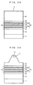
- Figs. 3, 4 and 5 are typical sectional views showing steps in a method of fabricating the semiconductor laser device shown in Fig. 1.
- MOCVD metal-organic chemical vapor deposition
- an SiO 2 film is formed on the p-type contact layer 7 and patterned for forming a striped SiO 2 film 17. Thereafter the p-type contact layer 7 and the p-type cladding layer 6 are partially removed by etching through the SiO 2 film 17 serving as a mask, for forming the ridge portion.
- the depletion enhancement layer 8 of Ga 0.5 In 0.5 P, the low carrier concentration layer 9 of GaAs and the current blocking layer 10 of n-GaAs are successively grown on the p-type cladding layer 6 by MOCVD through the SiO 2 film 17 serving as a selective growth mask.
- the SiO 2 film 17 is removed and thereafter the contact layer 11 of p-GaAs is formed on the n-type current blocking layer 10 and on the p-type contact layer 7 by MOCVD as shown in Fig. 1, while the p-electrode 12 of Cr/Au is formed on the surface of the p-type contact layer 11 and the n electrode 13 of AuGe/Ni/Au is formed on the back side of the n-GaAs substrate 1.
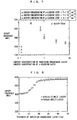
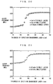
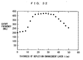
- Fig. 6 is a diagram showing the results of measurement of a cutoff frequency of the semiconductor laser device shown in Table 1 with variation of the thickness t of the depletion enhancement layer 8.
- the cutoff frequency is such a frequency that the amplitude of a laser beam superposed with a sine wave output from the object semiconductor laser device is reduced by 3 dB as compared with the case of superposing a low frequency (the superposed frequency is not more than 10 MHz in this example).
- ⁇ denotes a case of employing a depletion enhancement layer 8 of Ga 0.5 In 0.5 P having a single-layer structure
- ⁇ denotes a case of employing a depletion enhancement layer 8 of a superlattice structure alternately having (Al 0.7 Ga 0.3 ) 0.5 In 0.5 P barrier layers and Ga 0.5 In 0.5 P well layers (the thickness t is the sum of the thicknesses of the well layers)
- ⁇ denotes a case of employing a depletion enhancement layer 8 of Al 0.45 Ga 0.55 As having a single-layer structure respectively.
- Fig. 7 illustrates an effect of improving the cutoff frequency by doping the depletion enhancement layer 8 of the semiconductor laser device shown in Fig. 1.
- the horizontal axis shows the ratio of the carrier concentration of the depletion enhancement layer 8 to the carrier concentration of the p-type cladding layer 6, and the vertical axis shows the cutoff frequency.
- the depletion enhancement layer 8 of this semiconductor laser device is made of p-type GaInP, and the thickness t thereof is 25 nm.
- the effect of improving the cutoff frequency is small when the carrier concentration of the depletion enhancement layer 8 is higher than that of the p-type cladding layer 6, while a large effect of improving the cutoff frequency is attained when the carrier concentration of the depletion enhancement layer 8 is lower than that of the p-type cladding layer 6. Therefore, the carrier concentration of the depletion enhancement layer 8 is preferably lower than that of the p-type cladding layer 6.
- the structure of the semiconductor laser device according to the second embodiment is similar to that shown in Fig. 1, while the materials, thicknesses and carrier concentrations of respective layers are different from those in the first embodiment.
- Table 2 shows the materials, thicknesses and carrier concentrations of the respective layers forming the semiconductor laser device according to this embodiment.
- Fig. 8 illustrates results of measurement of a cutoff frequency of the semiconductor laser device shown in Table 2 with variation of the thickness t of a depletion enhancement layer 8.
- ⁇ denotes a case of employing a depletion enhancement layer 8 of Al 0.25 Ga 0.75 As having a single-layer structure
- ⁇ denotes a case of employing a depletion enhancement layer 8 of a superlattice structure alternately having Al 0.45 Ga 0.55 As barrier layers and Al 0.25 Ga 0.75 As well layers (the thickness t is the sum of the thicknesses of the well layers).
- the cutoff frequency, 400 MHz when the semiconductor laser device is formed with no depletion enhancement layer 8, is improved when the thickness t of the depletion enhancement layer 8 is increased, remarkably improved when the thickness t of the depletion enhancement layer 8 exceeds 10 nm, and substantially saturated when the thickness t is about 20 nm. Therefore, the thickness t of the depletion enhancement layer 8 is preferably at least 10 nm, and more preferably at least 20 nm saturating improvement of the cutoff frequency. When the thickness t of the depletion enhancement layer 8 is at least 15 nm, the intermediate level between 10 nm and 20 nm, the high-frequency characteristic can be sufficiently improved.
- a semiconductor laser device according to a third embodiment of the present invention is now described.
- the structure of the semiconductor laser device according to the third embodiment is similar to that shown in Fig. 1, while the materials, thicknesses and carrier concentrations of respective layers are different from those in the first embodiment.
- Table 3 shows the materials, thicknesses and carrier concentrations of the respective layers forming the semiconductor laser device according to this embodiment.
- Fig. 9 illustrates results of measurement of a cutoff frequency of the semiconductor laser device shown in Table 3 with variation of the thickness t of a depletion enhancement layer 8.
- ⁇ denotes a case of employing a depletion enhancement layer 8 of Al 0.07 Ga 0.93 N having a single-layer structure
- ⁇ denotes a case of employing a depletion enhancement layer 8 of a superlattice structure alternately having Al 0.15 Ga 0.85 N barrier layers and Al 0.07 Ga 0.93 N well layers (the thickness t is the sum of the thicknesses of the well layers).
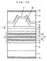
- Fig. 10 is a typical sectional view showing a semiconductor laser device according to a fourth embodiment of the present invention.
- respective layers 2 to 5 are formed on an n-GaAs substrate 1, similarly to the semiconductor laser device shown in Fig. 1.
- a cladding layer 61 of p-(Al 0.7 Ga 0.3 ) 0.5 In 0.5 P having a thickness of 200 nm and a depletion enhancement layer 62 of Ga 0.5 In 0.5 P are successively formed on the guide layer 5.
- the carrier concentration of the p-type cladding layer 61 is 3 ⁇ 10 17 cm -3 .
- a cladding layer 63 of p-(Al 0.7 Ga 0.3 ) 0.5 In 0.5 P of 1300 nm in thickness having a ridge shape is formed on the depletion enhancement layer 62.
- the carrier concentration of the p-type cladding layer 63 is 3 ⁇ 10 17 cm -3 .
- a contact layer 7 of p-Ga 0.5 In 0.5 P is formed on the upper surface of the p-type cladding layer 63.
- a low carrier concentration layer 9 of GaAs of 1000 nm in thickness having a striped opening on the upper surface of the p-type contact layer 7 is formed on portions of the depletion enhancement layer 62 located on both sides of the p-type cladding layer 63 and on the side surfaces of the p-type cladding layer 63.
- a current blocking layer 10 of n-GaAs of 500 nm in thickness having a striped opening on the upper surface of the ridge portion is formed on the low carrier concentration layer 9.
- a p-type contact layer 11 is formed on the p-type contact layer 7 and the n-type current blocking layer 10.
- Table 4 shows the aforementioned structure.
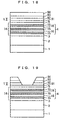
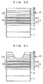
- Figs. 11, 12 and 13 are typical sectional views showing steps in a method of fabricating the semiconductor layer device shown in Fig. 10.
- an SiO 2 film is formed on the p-type contact layer 7 and patterned for forming a striped SiO 2 film 64. Thereafter the p-type contact layer 7 and the p-type cladding layer 63 are removed by etching through the SiO 2 film 64 serving as a mask, for forming the ridge portion.
- the low carrier concentration layer 9 of GaAs and the current blocking layer 10 of n-GaAs are successively grown on the side surfaces of the depletion enhancement layer 62 and the p-type cladding layer 63 located on both sides of the ridge portion by MOCVD through the SiO 2 film 64 serving as a selective growth mask.
- the SiO 2 film 64 is removed and thereafter the contact layer 11 of p-GaAs is formed on the n-type current blocking layer 10 and the p-type contact layer 7 by MOCVD, while forming a p-electrode 12 of Cr/Au on the surface of the p-type contact layer 11 and forming an n electrode 13 of AuGe/Ni/Au on the back side of the n-GaAs substrate 1, as shown in Fig. 10.
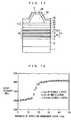
- Fig. 14 is a diagram showing the results of measurement of a cutoff frequency of the semiconductor laser device shown in Table 4 with variation of the thickness t of the depletion enhancement layer 62.
- ⁇ denotes a case of employing a depletion enhancement layer 62 of Ga 0.5 In 0.5 P having a single-layer structure
- the cutoff frequency 200 MHz when the semiconductor laser device is formed with no depletion enhancement layer 62, is gradually improved when the thickness t of the depletion enhancement layer 62 is increased, remarkably improved when the thickness t of the depletion enhancement layer 62 exceeds 15 nm, and substantially saturated when the thickness t is about 20 nm. Therefore, the thickness t of the depletion enhancement layer 62 is preferably at least 15 nm, and more preferably at least 20 nm saturating improvement of the cutoff frequency. When the thickness t of the depletion enhancement layer 62 is at least 18 nm, the intermediate level between 15 nm and 20 nm, the high-frequency characteristic can be sufficiently improved.
- a semiconductor laser device according to a fifth embodiment of the present invention is now described.
- the structure of the semiconductor laser device according to the fifth embodiment is similar to that shown in Fig. 10, except the material, thicknesses and carrier concentrations of respective layers.
- Table 5 shows the materials, thicknesses and carrier concentrations of the respective layers of the semiconductor laser device according to this embodiment.
- Fig. 15 is a diagram showing the results of measurement of a cutoff frequency of the semiconductor laser device shown in Table 5 with variation of the thickness t of a depletion enhancement layer 62.
- ⁇ denotes a case of employing a depletion enhancement layer 62 of Al 0.25 Ga 0.75 As having a single-layer structure
- ⁇ denotes a case of employing a depletion enhancement layer 62 of a superlattice structure alternately having Al 0.45 Ga 0.55 As barrier layers and Al 0.25 Ga 0.75 As well layers (the thickness t is the sum of the thicknesses of the well layers) respectively.
- a semiconductor laser device according to a sixth embodiment of the present invention is now described.
- the structure of the semiconductor laser device according to the sixth embodiment is similar to that shown in Fig. 10, except the materials, thicknesses and carrier concentrations of respective layers.
- Table 6 shows the materials, thicknesses and carrier concentrations of the respective layers of the semiconductor laser device according to this embodiment.
- Fig. 16 is a diagram showing the results of measurement of a cutoff frequency of the semiconductor laser device shown in Table 6 with variation of the thickness t of a depletion enhancement layer 62.
- ⁇ denotes a case of employing a depletion enhancement layer 62 of Al 0.07 Ga 0.93 N having a single-layer structure
- ⁇ denotes a case of employing a depletion enhancement layer 62 of a superlattice structure alternately having Al 0.15 Ga 0.85 N barrier layers and Al 0.07 Ga 0.93 N well layers (the thickness t is the sum of the thicknesses of the well layers) respectively.
- Fig. 17 is a typical sectional view of a semiconductor laser device according to a seventh embodiment of the present invention.
- respective layers 2 to 5 are formed on an n-GaAs substrate 1, similarly to the semiconductor laser device shown in Fig. 1.
- a cladding layer 91 of p-(Al 0.7 Ga 0.3 ) 0.5 In 0.5 P having a thickness of 200 nm is formed on the guide layer 5.
- the carrier concentration of the p-type cladding layer 91 is 3 x 10 17 cm -3 .
- a depletion enhancement layer 92 of Ga 0.5 In 0.5 P, a low carrier concentration 93 of GaAs having a thickness of 1000 nm and a current blocking layer 94 of n-GaAs having a thickness of 500 nm are successively formed on the p-type cladding layer 91.
- the carrier concentration of the n-type current blocking layer 94 is 8 ⁇ 10 17 cm -3 .
- the carrier concentration of the low carrier concentration layer 93 is lower than that of the n-type current blocking layer 94.
- the carrier concentration of the p-type cladding layer 95 is 3 ⁇ 10 17 cm -3 .
- a contact layer 96 of p-Ga 0.5 In 0.5 P having a thickness of 200 nm is formed on the p-type cladding layer 95.
- a contact layer 97 of p-GaAs having a thickness of 3000 nm is formed on the p-type contact layer 96.
- the carrier concentration of the p-type contact layer 96 is 2 ⁇ 10 18 cm -3 .
- the carrier concentration of the p-type contact layer 97 is 3 ⁇ 10 19 cm -3 .
- Table 7 shows the aforementioned structure.
- Figs. 18 and 19 are typical sectional views showing steps in a method of fabricating the semiconductor laser device shown in Fig. 17.
- a mask (not shown) is formed on the n-type current blocking layer 94 and patterned to have a striped opening. Thereafter the central portions of the n-type current blocking layer 94, the low carrier concentration layer 93 and the depletion enhancement layer 92 are removed by etching for forming the striped opening, as shown in Fig. 19.
- the cladding layer 95 of p-(Al 0.7 Ga 0.3 ) 0.5 In 0.5 P, the contact layer 96 of p-Ga 0.5 In 0.5 P and the contact layer 97 of p-GaAs are successively formed on the n-type current blocking layer 94 and on the p-type cladding layer 91 located in the striped opening by MOCVD, as shown in Fig. 17.
- a p-electrode 12 of Cr/Au is formed on the surface of the p-type contact layer 97, and an n electrode 13 of AuGe/Ni/Au is formed on the back side of the n-GaAs substrate 1.
- Fig. 20 is a diagram showing the results of measurement of a cutoff frequency of the semiconductor laser device shown in Table 7 with variation of the thickness t of the depletion enhancement layer 92.
- ⁇ denotes a case of employing a depletion enhancement layer 92 of Ga 0.5 In 0.5 P having a single-layer structure
- ⁇ denotes a case of employing a depletion enhancement layer 92 of a superlattice structure alternately having (Al 0.7 Ga 0.3 ) 0.5 In 0.5 P barrier layers and Ga 0.5 In 0.5 P well layers (the thickness t is the sum of the thicknesses of the well layers)
- ⁇ denotes a case of employing a depletion enhancement layer 92 of Al 0.45 Ga 0.55 As having a single-layer structure respectively.
- the cutoff frequency 200 MHz when the semiconductor laser device is formed with no depletion enhancement layer 92, is gradually improved when the thickness t of the depletion enhancement layer 92 is increased, remarkably improved when the thickness t of the depletion enhancement layer 92 exceeds 10 nm, and substantially saturated when the thickness t is about 20 nm. Therefore, the thickness t of the depletion enhancement layer 92 is preferably at least 15 nm, and more preferably at least 20 nm saturating improvement of the cutoff frequency. When the thickness t of the depletion enhancement layer 92 is at least 18 nm, the intermediate level between 15 nm and 20 nm, the high-frequency characteristic can be sufficiently improved.
- a semiconductor laser device according to an eighth embodiment of the present invention is now described.
- the structure of the semiconductor laser device according to the eighth embodiment is similar to that shown in Fig. 17, except the materials, thicknesses and carrier concentrations of respective layers.
- Table 8 shows the materials, thicknesses and carrier concentrations of the respective layers in the semiconductor laser device according to this embodiment.
- Fig. 21 is a diagram showing the results of measurement of a cutoff frequency of the semiconductor laser device shown in Table 8 with variation of the thickness t of a depletion enhancement layer 92.
- ⁇ denotes a case of employing a depletion enhancement layer 92 of Al 0.25 Ga 0.75 As having a single-layer structure
- ⁇ denotes a case of employing a depletion enhancement layer 92 of a superlattice structure alternately having Al 0.45 Ga 0.75 As barrier layers and Al 0.25 Ga 0.75 As well layers (the thickness t is the sum of the thicknesses of the well layers) respectively.
- a semiconductor laser device according to a ninth embodiment of the present invention is now described.
- the structure of the semiconductor laser device according to the ninth embodiment is similar to that shown in Fig. 17, except the materials, thicknesses and carrier concentrations of respective layers.
- Table 9 shows the materials, thicknesses and carrier concentrations of the respective layers in the semiconductor laser device according to this embodiment.
- Fig. 22 is a diagram showing the results of measurement of a cutoff frequency of the semiconductor laser device shown in Table 9 with variation of the thickness t of a depletion enhancement layer 92.
- ⁇ denotes a case of employing a depletion enhancement layer 92 of Al 0.07 Ga 0.93 N having a single-layer structure
- ⁇ denotes a case of employing a depletion enhancement layer 92 of a superlattice structure alternately having Al 0.15 Ga 0.85 N barrier layers and Al 0.07 Ga 0.93 N well layers (the thickness t is the sum of the thicknesses of the well layers) respectively.
- the cutoff frequency 320 MHz when the semiconductor laser device is formed with no depletion enhancement layer 92, is gradually improved when the thickness t of the depletion enhancement layer 92 is increased, remarkably improved when the thickness t of the depletion enhancement layer 92 exceeds 15 nm, and substantially saturated when the thickness t is about 20 nm. Therefore, the thickness t of the depletion enhancement layer 92 is preferably at least 15 nm, and more preferably at least 20 nm saturating improvement of the cutoff frequency. When the thickness t of the depletion enhancement layer 92 is at least 18 nm, the intermediate level between 15 nm and 20 nm, the high-frequency characteristic can be sufficiently improved.
- the materials for the active layer, the depletion enhancement layer, the low carrier concentration layer and the current blocking layer are not restricted to those in the aforementioned embodiments.
- any arbitrary combination of an active layer of (Al x1 Ga 1-x1 ) y1 In 1-y1 P, a depletion enhancement layer of (Al x2 Ga 1-x2 ) y2 In 1-y2 P or Al x2 Ga 1-x2 As, a low carrier concentration layer of (Al x3 Ga 1-x3 ) y3 In 1-y3 P or Al x3 Ga 1-x3 As and a current blocking layer of (Al x4 Ga 1-x4 ) y4 In 1-y4 P or Al x4 Ga 1- x4 AS can be employed.
- Each of x1, x2, x3, x4, y1, y2, y3 and y4 is at least zero and not more than 1.
- Fig. 23 is a typical sectional view of a semiconductor laser device according to a tenth embodiment of the present invention.
- a cladding layer 2 of n-(Al 0.7 Ga 0.3 ) 0.5 In 0.5 P having a thickness of 1500 nm and an emission layer 14 described later are successively formed on an n-GaAs substrate 1.
- a cladding layer 6 of p-(Al 0.7 Ga 0.3 ) 0.5 In 0.5 P having a thickness of 1500 nm and a contact layer 7 of p-Ga 0.5 In 0.5 P having a thickness of 200 nm are successively formed on the emission layer 14.
- the p-type cladding layer 6 and the p-type contact layer 7 are etched for defining a ridge portion.
- the carrier concentration of the n-GaAs substrate 1 is 1 ⁇ 10 18 cm -3
- the carrier concentration of the n-type cladding layer 2 is 3 ⁇ 10 17 cm -3
- the carrier concentration of the p-type cladding layer 6 is 3 x 10 17 cm -3
- the carrier concentration of the p-type contact layer 7 is 2 x 10 18 cm -3 .
- a n-type depletion enhancement layer 8n of n-GaAs having a thickness t, having a striped opening on the upper surface of the ridge portion is formed on the p-type cladding layer 6.
- a reverse conduction type second current blocking layer 10 of n-GaAs of 500 nm in thickness having a striped opening on the upper surface of the ridge portion is formed on the first current blocking layer 9 having a low carrier concentration.
- the carrier concentration of the n-type depletion enhancement layer 8n is 5 ⁇ 10 17 cm -3 .
- the carrier concentration of the second current blocking layer 10 is 8 ⁇ 10 17 cm -3 .
- a contact layer 11 of p-GaAs having a thickness of 3000 nm is formed on the p-type contact layer 7 located in the striped opening of the second current blocking layer 10 and on the second current blocking layer 10.
- the carrier concentration of the p-type contact layer 11 is 3 x 10 19 cm -3 .
- a p-electrode 12 having a thickness of 300 nm is formed on the p-type contact layer 11.
- An n electrode 13 having a thickness of 300 nm is formed on the back side of the n-GaAs substrate 1.
- the semiconductor laser device shown in Fig. 23 has a ridge guided structure.
- the emission layer 14 includes a guide layer 3 of (Al 0.5 Ga 0.5 ) 0.5 In 0.5 P having a thickness of 30 nm formed on the n-type cladding layer 2, a quantum well active layer 4 formed on the guide layer 3 and a guide layer 5 of (Al 0.5 Ga 0.5 ) 0.5 In 0.5 P having a thickness of 30 nm formed on the quantum well layer 4.
- the quantum well active layer 4 has a superlattice structure formed by alternately stacking a plurality of quantum well layers 15 of Ga 0.5 In 0.5 P each having a thickness of 5 nm and a plurality of barrier layers 16 of (Al 0.5 Ga 0.5 ) 0.5 In 0.5 P each having a thickness of 5 nm.
- the number of the barrier layers 16 is 2,and the number of the quantumwell layers 15 is 3.
- Table 10 shows the aforementioned structure.
- Figs. 24(a) and 24 (b) typically show energy band diagrams of the p-type cladding layer 6, the n-type depletion enhancement layer 8 and the first current blocking layer 9 having a low carrier concentration in the semiconductor laser device shown in Fig. 23.
- the band gap of the n-type depletion enhancement layer 8n and that of the first current blocking layer 9 having a low carrier concentration are equal to each other, and the band gaps of these layers 8n and 9 are smaller than that of the p-type cladding layer 6.
- the first current blocking layer 9 having a low carrier concentration is kept in a depleted state due to such reduction of the quantity of carriers stored therein, whereby electric capacitance generated between the first current blocking layer 9 having a low carrier concentration and the p-type cladding layer 6 can be reduced for sufficiently increasing the operating speed of the semiconductor laser device.
- the high-frequency characteristic of the semiconductor laser device shown in Fig. 23 is readily improved by forming the n-type depletion enhancement layer 8 formed with the impurity levels of the opposite conduction type to the p-type cladding layer 6 between the p-type cladding layer 6 and the first current blocking layer 9 having a low carrier concentration.
- Figs. 25, 26 and 27 are typical sectional views showing steps in a method of fabricating the semiconductor laser device shown in Fig. 23.
- an SiO 2 film is formed on the p-type contact layer 7 and patterned for forming a striped SiO 2 film 17. Thereafter the p-type contact layer 7 and the p-type cladding layer 6 are partially removed by etching through the SiO 2 film 17 serving as a mask, for defining the ridge portion.
- the depletion enhancement layer 8n of n-GaAs, the first current blocking layer 9 of undoped GaAs having a low carrier concentration and the second current blocking layer 10 of n-GaAs are successively formed on the p-type cladding layer 6 by MOCVD through the SiO 2 film 17 serving as a selective growth mask.
- the SiO 2 film 17 is removed and thereafter the contact layer 11 of p-GaAs is formed on the second current blocking layer 10 and the p-type contact layer 7 by MOCVD, while the p-electrode 12 of Cr/Au is formed on the surface of the p-type contact layer 11 and the n electrode 13 of AuGe/Ni/Au is formed on the back side of the n-GaAs substrate 1 as shown in Fig. 23.
- the thickness t of the depletion enhancement layer 8n having a carrier concentration of 5 ⁇ 10 17 cm -3 is varied for measuring the cutoff frequency of the semiconductor laser device at each level of the thickness t. Consequently, it is proved that the cutoff frequency is remarkably improved when the thickness t of the n-type depletion enhancement layer 8n is in the range of 20 to 35 nm.
- the thickness t of the n-type depletion enhancement layer 8n is set to 30 nm and the carrier concentration thereof is varied for measuring the cutoff frequency of the semiconductor laser device at each level of the carrier concentration. Consequently, it is provided that the cutoff frequency is remarkably improved when the carrier concentration of the n-type depletion enhancement layer 8n is in the range of 3 x 10 17 to 6 x 10 17 cm -3 .
- a semiconductor laser device according to an eleventh embodiment of the present invention is now described.
- the structure of the semiconductor laser device according to the eleventh embodiment is similar to that shown in Fig. 23, except the materials, thicknesses and carrier concentrations of respective layers.
- Table 11 shows the materials, thicknesses and carrier concentrations of the respective layers of the semiconductor laser device according to this embodiment.
- an n-type depletion enhancement layer 8n formed with impurity levels (donor levels) of the opposite conduction type to a p-type cladding layer 6 is formed between the p-type cladding layer 6 and a first current blocking layer 9 having a low carrier concentration in the semiconductor laser device according to this embodiment.
- carriers supplied from the donor levels formed on the n-type depletion enhancement layer 8n compensate for those supplied from the p-type cladding layer 6, similarly to the tenth embodiment. Therefore, the quantity of carriers stored in the first current blocking layer 9 having a low carrier concentration is reduced.
- the first current blocking layer 9 having a low carrier concentration is kept in a depleted state due to such reduction of the quantity of carriers stored therein, whereby electric capacitance generated between the first current blocking layer 9 having a low carrier concentration and the p-type cladding layer 6 can be reduced for sufficiently increasing the operating speed of the semiconductor laser device.
- the high-frequency characteristic of the semiconductor laser device is readily improved in this embodiment.
- the semiconductor laser device is so set that the band gap of the n-type depletion enhancement layer 8n is smaller than that of the p-type cladding layer 6 and larger than that of the first current blocking layer 9 having a low carrier concentration.
- the n-type depletion enhancement layer 8n according to this embodiment also has a function as an intermediate band gap layer described later with reference to a thirteenth embodiment.
- the band gaps of the p-type cladding layer 6, the n-type depletion enhancement layer 8n and the first current blocking layer 9 having a low carrier concentration are reduced in this order. Therefore, the band offset between the p-type cladding layer 6 and the n-type depletion enhancement layer 8n is smaller than that between the p-type cladding layer 6 and the first current blocking layer 9 having a low carrier concentration.
- carriers are hardly injected from the p-type cladding layer 6 into the n-type depletion enhancement layer 8n, and hardly injected into the first current blocking layer 9 having a low carrier concentration either.
- carriers are injected into both of the n-type depletion enhancement layer 8n and the first current blocking layer 9 having a low carrier concentration in a divided manner, whereby the quantity of carriers injected into the first current blocking layer 9 having a low carrier concentration is reduced.
- the quantity of carriers stored in the first current blocking layer 9 having a low carrier concentration can be further reduced by forming the n-type depletion enhancement layer 8n having the intermediate band gap between the p-type cladding layer 6 and the first current blocking layer 9 having a low carrier concentration.
- electric capacitance generated between the first current blocking layer 9 having a low carrier concentration and the p-type cladding layer 6 can be further reduced in the embodiment having the n-type depletion enhancement layer 8n, having the intermediate band gap between the p-type cladding layer 6 and the first current blocking layer 9 having a low carrier concentration, whereby the operating speed of the semiconductor laser device is further improved.
- the thickness t of the n-type depletion enhancement layer 8n having a carrier concentration of 5 ⁇ 10 17 cm -3 is varied for measuring the cutoff frequency of the semiconductor laser device at each level of the thickness t. Consequently, it is proved that the cutoff frequency is remarkably improved when the thickness t of the n-type depletion enhancement layer 8n is in the range of 10 to 40 nm.
- the thickness t of the n-type depletion enhancement layer 8n is set to 25 nm and the carrier concentration thereof is varied for measuring the cutoff frequency of the semiconductor laser device at each level of the carrier concentration. Consequently, it is proved that the cutoff frequency is remarkably improved when the carrier concentration of the n-type depletion enhancement layer 8n is in the range of 2.5 ⁇ 10 17 to 8.5 ⁇ 10 17 cm -3 .
- the n-type depletion enhancement layer 8n has the intermediate band gap between the p-type cladding layer 6 and the first current blocking layer 9 having a low carrier concentration in this embodiment, whereby the ranges of the thickness and the carrier concentration of the n-type depletion enhancement layer 8n capable of remarkably improving the cutoff frequency of the semiconductor laser device are widened as compared with the first embodiment provided with the n-type depletion enhancement layer 8 and the first current blocking layer 9 of a low carrier concentration having the same band gaps.
- the thickness and the carrier concentration of the n-type depletion enhancement layer 8n can be readily set and the n-type depletion enhancement layer 8n can be readily prepared.
- an undoped layer may be formed between the n-type depletion enhancement layer 8n and the p-type cladding layer 6.
- an undoped layer may be formed between the n-type depletion enhancement layer 8n and the first current blocking layer 9 having a low carrier concentration.
- an undoped layer made of a material having a larger band gap than the first current blocking layer 9 having a low carrier concentration is preferably formed.
- the material for the undoped layer preferably has a band gap smaller than that of the p-type cladding layer 6 and larger than that of the first current blocking layer 9 having a low carrier concentration.
- the structure of the semiconductor laser device according to the twelfth embodiment is similar to that shown in Fig. 23, except the materials, thicknesses and carrier concentrations of respective layers.
- Table 12 shows the materials, thicknesses and carrier concentrations of the respective layers of the semiconductor laser device according to this embodiment.
- a n-type depletion enhancement layer 8n formed with n impurity levels (donor levels) of the opposite conduction type to a p-type cladding layer 6 is formed between the p-type cladding layer 6 and a first current blocking layer 9 having a low carrier concentration in the semiconductor laser device according to this embodiment.
- carriers supplied from the donor levels formed on the n-type depletion enhancement layer 8n compensate for those supplied from the p-type cladding layer 6, similarly to the tenth embodiment. Therefore, the quantity of carriers stored in the first current blocking layer 9 having a low carrier concentration is reduced.
- the band gap of the n-type depletion enhancement layer 8n and that of the first current blocking layer 9 having a low carrier concentration are equal to each other, and the band gaps of these layers 8n and 9 are smaller than that of the p-type cladding layer 6.
- the first current blocking layer 9 having a low carrier concentration is kept in a depleted state due to reduction of the quantity of carriers stored therein, whereby electric capacitance generated between the first current blocking layer 9 having a low carrier concentration and the p-type cladding layer 6 can be reduced for sufficiently increasing the operating speed of the semiconductor laser device. In this embodiment, therefore, the high-frequency characteristic of the semiconductor laser device is improved.
- the thickness t of the n-type depletion enhancement layer 8n having a carrier concentration of 5 x 10 17 cm -3 is varied for measuring the cutoff frequency of the semiconductor laser device at each level of the thickness t. Consequently, it is proved that the cutoff frequency is remarkably improved when the thickness t of the n-type depletion enhancement layer 8n is 35 nm.
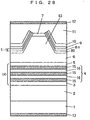
- Fig. 28 is a typical sectional view showing a semiconductor laser device according to a thirteenth embodiment of the present invention.
- the structure of the semiconductor laser device shown in Fig. 28 is similar to that of the semiconductor laser device shown in Fig. 23 except the following point:
- an intermediate band gap layer 80 having a band gap smaller than that of a p-type cladding layer 6 and larger than that of a n-type depletion enhancement layer 8n is formed between the p-type cladding layer 6 and the n-type depletion enhancement layer 8n.
- Table 13 shows the structure of the semiconductor laser device shown in Fig. 28.
- the n-type depletion enhancement layer 8n formed with n impurity levels (donor levels) of the opposite conduction type to the p-type cladding layer 6 is formed between the p-type cladding layer 6 and a first current blocking layer 9 having a low carrier concentration in the semiconductor laser device according to this embodiment.
- carriers supplied from the donor levels formed on the n-type depletion enhancement-layer 8n compensate for those supplied from the p-type cladding layer 6, similarly to the tenth embodiment. Therefore, the quantity of carriers stored in the first current blocking layer 9 having a low carrier concentration is reduced.
- the first current blocking layer 9 having a low carrier concentration is kept in a depleted state due to such reduction of the quantity of carriers stored therein, whereby electric capacitance generated between the first current blocking layer 9 having a low carrier concentration and the p-type cladding layer 6 can be reduced for sufficiently increasing the operating speed of the semiconductor laser device.
- the high-frequency characteristic of the semiconductor laser device is improved in the present invention.
- the band gap of the n-type depletion enhancement layer 8n and that of the first current blocking layer 9 having a low carrier concentration are equal to each other, and the band gaps of these layers 8n and 9 are smaller than that of the p-type cladding layer 6.
- the intermediate band gap layer 80 having the intermediate band gap between the p-type cladding layer 6 and the n-type depletion enhancement layer 8n is formed between the p-type cladding layer 6 and the n-type depletion enhancement layer 8n.
- the embodiment having such an intermediate band gap layer 80 attains the following effect:
- the band gaps of the p-type cladding layer 6, the intermediate band gap layer 8 and the n-type depletion enhancement layer 8n are reduced in this order, whereby the band offset between the p-type cladding layer 6 and the intermediate band gap layer 80 is smaller than that between the p-type cladding layer 6 and the n-type depletion enhancement layer 8n.
- carriers are hardly injected from the p-type cladding layer 6 into the intermediate band gap layer 80, and hardly injected into the n-type depletion enhancement layer 8n either.
- carriers are injected into both of the intermediate band gap layer 80 and the n-type depletion enhancement layer 8n in a divided manner, whereby the quantity of carriers injected into the n-type depletion enhancement layer 8n is reduced.
- the quantities of carriers injected into the n-type depletion enhancement layer 8n as well as those injected into the first current blocking layer 9 having a low carrier concentration can be reduced by forming the intermediate band gap layer 80. Therefore, the quantity of carriers stored in the first current blocking layer 9 having a low carrier concentration can be further reduced.
- electric capacitance generated between the first current blocking layer 9 having a low carrier concentration and the p-type cladding layer 6 can be further reduced, thereby more improving the operating speed of the semiconductor laser device.
- the thickness t of the n-type depletion enhancement layer 8n having a carrier concentration of 5 ⁇ 10 17 cm -3 is varied for measuring the cutoff frequency of the semiconductor laser device at each level of the thickness t. Consequently, it is proved that the cutoff frequency is remarkably improved when the thickness t of the n-type depletion enhancement layer 8n is in the range of 15 to 35 nm.
- the thickness t of the n-type depletion enhancement layer 8n was set to 30 nm and the carrier concentration thereof is varied for measuring the cutoff frequency of the semiconductor laser device at each level of the carrier concentration. Consequently, it is proved that the cutoff frequency is remarkably improved when the carrier concentration of the n-type depletion enhancement layer 8n is in the range of 2.5 ⁇ 10 17 to 6 ⁇ 10 17 cm -3 .
- the ranges of the thickness t and the carrier concentration of the n-type depletion enhancement layer 8n capable of remarkably improving the cutoff frequency of the semiconductor laser device are widened in the embodiment provided with the intermediate band gap layer 80 as compared with the first embodiment having no intermediate band gap layer. Therefore, the thickness t and the carrier concentration of the n-type depletion enhancement layer 8n can be readily set and the n-type depletion enhancement layer 8n can be readily prepared.
- Fig. 29 is a typical sectional view of a semiconductor laser device according to a fourteenth embodiment of the present invention.
- respective layers 2 to 5 are formed on an n-GaAs substrate 1, similarly to the semiconductor laser device shown in Fig. 23.
- a cladding layer 91 of p-(Al 0.7 Ga 0.3 ) 0.5 In 0.5 P having a thickness of 200 nm is formed on the guide layer 5.
- the carrier concentration of the p-type cladding layer 91 is 3 ⁇ 10 17 cm -3 .
- Central regions of the n-type depletion enhancement layer 92n, the first current blocking layer 93 having a low carrier concentration layer and the second current blocking layer 94 are removed to define a striped opening.
- the carrier concentration of the n-type depletion enhancement layer 92n is 5 ⁇ 10 17 cm -3 .
- the carrier concentration of the second current blocking layer 94 is 8 ⁇ 10 17 cm -3 .
- a cladding layer 95 of p-(Al 0.7 Ga 0.3 ) 0.5 In 0.5 P having a thickness of 1300 nm is formed on the p-type cladding layer 91 and the second current blocking layer 94 to fill up the striped opening.
- the carrier concentration of the p-type cladding layer 95 is 3 x 10 17 cm -3 .
- a contact layer 96 of p-Ga 0.5 In 0.5 P having a thickness of 200 nm is formed on the p-type cladding layer 95.
- a contact layer 97 of p-GaAs having a thickness of 3000 nm is formed on the p-type contact layer 96.
- the carrier concentration of the p-type contact layer 96 is 2 ⁇ 10 18 cm -3 .
- the carrier concentration of the p-type contact layer 97 is 3 ⁇ 10 19 cm -3 .
- Table 14 shows the aforementioned structure.
- Figs. 30 and 31 are typical sectional views showing steps in a method of fabricating the semiconductor laser device shown in Fig. 29.
- a mask (not shown) is formed on the second current blocking layer 94 and patterned to have a striped opening. Thereafter the central portions of the second current blocking layer 94, the first current blocking layer 93 having a low carrier concentration and the depletion enhancement layer 92n are removed by etching for forming the striped opening, as shown in Fig. 31.
- the cladding layer 95 of p-(Al 0.7 Ga 0.3 ) 0.5 In 0.5 P, the contact layer 96 of p-Ga 0.5 In 0.5 P and the contact layer 97 of p-GaAs are successively formed on the second current blocking layer 94 and on the p-type cladding layer 91 located in the striped opening by MOCVD, as shown in Fig. 29.
- a p-electrode 12 of Cr/Au is formed on the surface of the p-type contact layer 97, and an n electrode 13 of AuGe/Ni/Au is formed on the back side of the n-GaAs substrate 1.
- the n-type depletion enhancement layer 92n formed with impurity levels (donor levels) of the opposite conduction type to the p-type cladding layer 91 is formed between the p-type cladding layer 91 and the first current blocking layer 93 having a low carrier concentration.
- carriers supplied from the donor levels formed on the n-type depletion enhancement layer 92n compensate for those supplied from the p-type cladding layer 91, similarly to the tenth embodiment. Therefore, the quantity of carriers stored in the first current blocking layer 93 having a low carrier concentration is reduced.
- the first current blocking layer 93 having a low carrier concentration is kept in a depleted state due to such reduction of the quantity of carriers stored therein, whereby electric capacitance generated between the first current blocking layer 93 having a low carrier concentration and the p-type cladding layer 91 can be reduced for sufficiently increasing the operating speed of the semiconductor laser device.
- the high-frequency characteristic of the semiconductor laser device is improved in this embodiment.
- the thickness t of the n-type depletion enhancement layer 92n having a carrier concentration of 5 x 10 17 cm -3 is varied for measuring the cutoff frequency of the semiconductor laser device at each level of the thickness t. Consequently, it is proved that the cutoff frequency is remarkably improved when the thickness t of the n-type depletion enhancement layer 92n is in the range of 20 to 35 nm.
- the thickness t of the n-type depletion enhancement layer 92n is set to 30 nm and the carrier concentration thereof is varied for measuring the cutoff frequency of the semiconductor laser device at each level of the carrier concentration. Consequently, it is proved that the cutoff frequency is remarkably improved when the carrier concentration of the n-type depletion enhancement layer 92n is in the range of 3 x 10 17 to 6 x 10 17 cm -3 .
- a semiconductor laser device according to a fifteenth embodiment of the present invention is now described.
- the structure of the semiconductor laser device according to the fifteenth embodiment is similar to that shown in Fig. 29, except the materials, thicknesses and carrier concentrations of respective layers.
- Table 15 shows the materials, thicknesses and carrier concentrations of the respective layers of the semiconductor laser device according to this embodiment.
- an-type depletion enhancement layer 92n formed with impurity levels (donor levels) of the opposite conduction type to a p-type cladding layer 91 is formed between the p-type cladding layer 91 and a first current blocking layer 93 having a low carrier concentration in the semiconductor laser device according to this embodiment.
- carriers supplied from the donor levels formed on the n-type depletion enhancement layer 92n compensate-for those supplied from the p-type cladding layer 91, similarly to the tenth embodiment. Therefore, the quantity of carriers stored in the first current blocking layer 93 having a low carrier concentration is reduced.
- the first current blocking layer 93 having a low carrier concentration is kept in a depleted state due to such reduction of the quantity of carriers stored therein, whereby electric capacitance generated between the first current blocking layer 93 having a low carrier concentration and the p-type cladding layer 91 can be reduced for sufficiently increasing the operating speed of the semiconductor laser device.
- the high-frequency characteristic of the semiconductor laser device is improved in this embodiment.
- Fig. 32 is a diagram showing the results of measurement of a cutoff frequency of the semiconductor laser device shown in Table 15 with variation of the thickness t of the n-type depletion enhancement layer 92n.
- the carrier concentration of the n-type depletion enhancement layer 92n is 5 x 10 17 cm -3 .
- the thickness t of the n-type depletion enhancement layer 92n is set to 25 nm and the carrier concentration thereof is varied for measuring the cutoff frequency of the semiconductor laser device at each level of the carrier concentration. Consequently, it is proved that the cutoff frequency is remarkably improved when the carrier concentration of the n-type depletion enhancement layer 92n is in the range of 3.5 ⁇ 10 17 to 8 ⁇ 10 17 cm -3 .
- a semiconductor laser device according to a sixteenth embodiment of the present invention is now described.
- the structure of the semiconductor laser device according to the sixteenth embodiment is similar to that shown in Fig. 29, except the materials, thicknesses and carrier concentrations of respective layers.
- Table 16 shows the materials, thicknesses and carrier concentrations of the respective layers of the semiconductor laser device according to this embodiment.
- an-type depletion enhancement layer 92n formed with impurity levels (donor levels) of the opposite conduction type to a p-type cladding layer 91 is formed between the p-type cladding layer 91 and a first current blocking layer 93 having a low carrier concentration in the semiconductor laser device according to this embodiment.
- carriers supplied from the donor levels formed in the n-type depletion enhancement layer 92n compensate for those supplied from the p-type cladding layer 91, similarly to the tenth embodiment. Therefore, the quantity of carriers stored in the first current blocking layer 93 having a low carrier concentration is reduced.
- the first current blocking layer 93 having a low carrier concentration is kept in a depleted state due to such reduction of the quantity of carriers stored therein, whereby electric capacitance generated between the first current blocking layer 93 having a low carrier concentration and the p-type cladding layer 91 can be reduced for sufficiently increasing the operating speed of the semiconductor laser device.
- the high-frequency characteristic of the semiconductor laser device is improved in this embodiment.
- the semiconductor laser device is so set that the band gap of the n-type depletion enhancement layer 92n is smaller than that of the p-type cladding layer 91 and larger than that of the first current blocking layer 93 having a low carrier concentration.
- the n-type depletion enhancement layer 92n according to this embodiment also has the function as the intermediate band gap layer 80 in the thirteenth embodiment.
- the band gaps of the p-type cladding layer 91, the n-type depletion enhancement layer 92n and the first current blocking layer 93 having a low carrier concentration are reduced in this order. Therefore, the band offset between the p-type cladding layer 91 and the n-type depletion enhancement layer 92n is smaller than that between the p-type cladding layer 91 and the first current blocking layer 93 having a low carrier concentration.
- carriers are hardly injected from the p-type cladding layer 91 into the n-type depletion enhancement layer 92n, and hardly injected into the first current blocking layer 93 having a low carrier concentration either.
- carriers are injected into both of the n-type depletion enhancement layer 92n and the first current blocking layer 93 having a low carrier concentration in a divided manner, whereby the quantity of carriers injected into the first current blocking layer 93 having a low carrier concentration is reduced.
- the quantity of carriers stored in the first current blocking layer 93 having a low carrier concentration can be further reduced by forming the n-type depletion enhancement layer 92n also serving as the intermediate band gap layer.
- electric capacitance generated between the first current blocking layer 93 having a low carrier concentration and the p-type cladding layer 91 can be further reduced in the embodiment having the n-type depletion enhancement layer 92n also serving as the intermediate band gap layer, whereby the operating speed of the semiconductor laser device is further improved.
- the thickness t of the n-type depletion enhancement layer 92n having a carrier concentration of 5 x 10 17 cm -3 is varied for measuring the cutoff frequency of the semiconductor laser device at each level of the thickness t. Consequently, it is proved that the cutoff frequency is remarkably improved when the thickness t of the n-type depletion enhancement layer 92n is 40 nm.
- an undoped layer may be formed between the n-type depletion enhancement layer 92n and the p-type cladding layer 91.
- an undoped layer may be formed between the n-type depletion enhancement layer 92n and the first current blocking layer 93 having a low carrier concentration.
- an undoped layer made of a material having a larger band gap than the first current blocking layer 93 having a low carrier concentration is preferably formed.
- the material for the undoped layer preferably has a band gap smaller than that of the p-type cladding layer 91 and larger than that of the first current blocking layer 93 having a low carrier concentration.
- the donor levels are formed on the depletion enhancement layer by doping the same with an n-type impurity.
- the donor levels formed on the depletion enhancement layer are preferably set to such density that most of the donor levels ionize in a state applying no bias voltage voltage.
- the n-type depletion enhancement layer of the opposite conduction type is formed on the region of the p-type cladding layer excluding the current injection region in each of the aforementioned tenth to sixteenth embodiments
- the n-type depletion enhancement layer may alternatively be formed on the current injection region of the p-type cladding layer. In this case, however, the thickness of the n-type depletion enhancement layer is reduced not to inhibit the current injection.
- the reverse conduction type second current blocking layer is provided on the first current blocking layer having a low carrier concentration in each of the aforementioned tenth to sixteenth embodiments, the reverse conduction type second current blocking layer is not necessarily required in the present invention but only the first current blocking layer having a low carrier concentration may be formed as the current blocking layer.
- the semiconductor laser device is prepared from a group III nitride semiconductor, an AlGaInP based semiconductor or an AlGaAs based semiconductor in each of the aforementioned tenth to sixteenth embodiments, the present invention is also applicable to other group III-V, group II-VI, group IV and group IV-IV semiconductors such as GaInAs.
- the present invention is particularly effective for a semiconductor laser device employing a semiconductor such as a group III nitride semiconductor, an AlGaInP based semiconductor or an AlGaAs based semiconductor, for example, hardly allowing formation of a semi-insulating semiconductor during epitaxy.
- ⁇ c represents the dielectric constant of a cladding layer
- ⁇ represents the dielectric constant of a depletion enhancement layer
- N c represents the carrier concentration of the cladding layer
- N represents the carrier concentration of the depletion enhancement layer
- E gc represents the band gap of the cladding layer
- ⁇ E v represents the valence band discontinuity at interface of the cladding layer and the depletion enhancement layer
- ⁇ E c represents the quantity of conduction band discontinuity between the cladding layer and the depletion enhancement layer.
- the cladding layer is of the n type and acceptor levels are formed on the depletion enhancement layer, as shown in Figs. 33(a) and 33(b).
- the energy of the lowest portion (the interface between the depletion enhancement layer and the cladding layer) of the conduction band of the depletion enhancement layer is equal to that of the lowest portion of the conduction band of the cladding layer. Therefore, no carriers are stored on the interface between the conduction band of the depletion enhancement layer and that of the gadding layer.
- the energy of the highest portion (the interface between the depletion enhancement layer and a first current blocking layer having a low carrier concentration) of the valence band of the depletion enhancement layer is equal that of the lowest portion of the conduction band of the cladding layer. Therefore, all acceptor levels of the depletion enhancement layer ionize to supply no carriers the current blocking layer having a low carrier concentration.
- the thickness t of the depletion enhancement layer is in the range of t A ⁇ t ⁇ t B , the quantity of charges stored on the interface between the cladding layer and the depletion enhancement layer remains unchanged with respect to small change of an electric field applied to the interface. In other words, transient electric capacitance can be approximated to zero on the interface between the cladding layer and the depletion enhancement layer.
- the thickness t of the depletion enhancement layer is preferably set in the aforementioned range in particular.
- ⁇ c is substantially equal to ⁇
- ⁇ E c is less than the band gap (E gc - ⁇ E c - ⁇ E v ) of the depletion enhancement layer.
- ⁇ c N c ⁇ E c / ( ⁇ N) may be greater than E gc - ⁇ E v - ⁇ E c when N c » N
- the relation ⁇ c N c ⁇ E c / ( ⁇ N) ⁇ E gc - ⁇ E c - ⁇ E v can be readily satisfied when N » N c or N is substantially equal to N c .
- the cladding layer is of the n type and the acceptor levels are formed on the depletion enhancement layer has been considered in the above discussion, a similar effect is attained also when the cladding layer is of the p type and the depletion enhancement layer is formed with donor levels as in the aforementioned embodiments.
- the thickness t of the depletion enhancement layer formed with the donor levels is preferably set in the aforementioned range in particular.
- the carrier concentration N c of the p-type cladding layer and the carrier concentration N of the depletion enhancement layer formed with the donor levels further preferably satisfy N c ⁇ N.
Landscapes
- Physics & Mathematics (AREA)
- Condensed Matter Physics & Semiconductors (AREA)
- General Physics & Mathematics (AREA)
- Electromagnetism (AREA)
- Optics & Photonics (AREA)
- Geometry (AREA)
- Semiconductor Lasers (AREA)
Abstract
Description
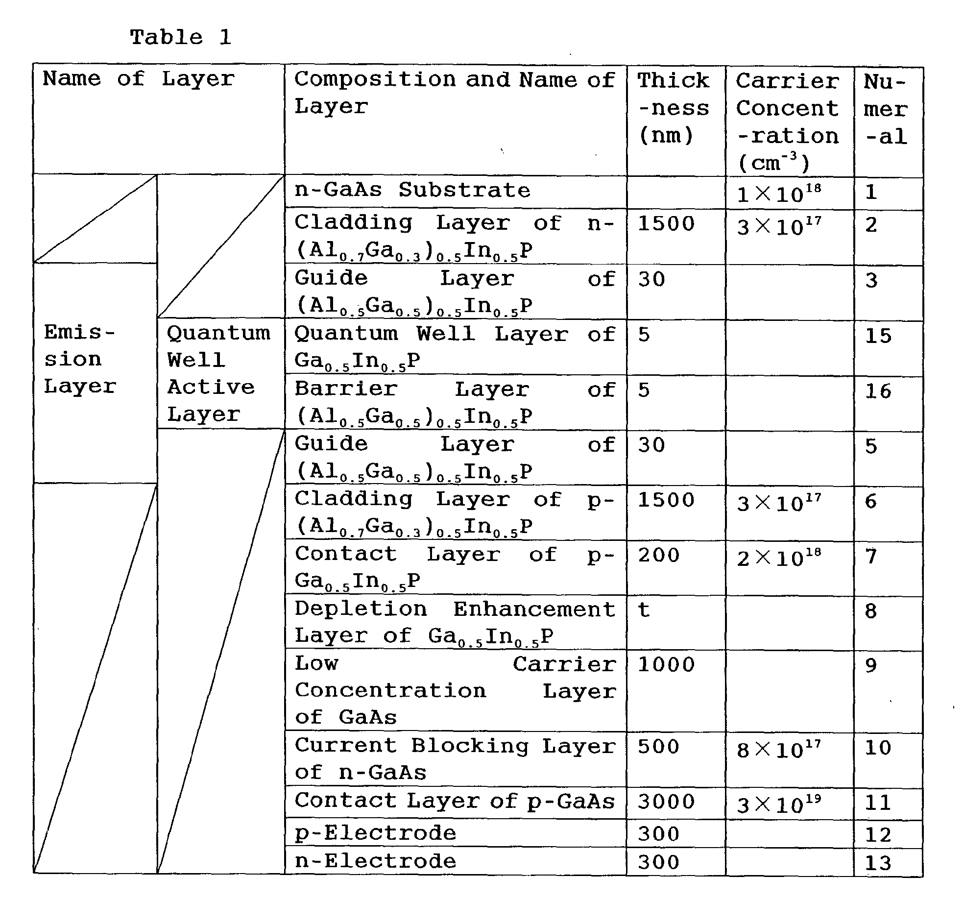


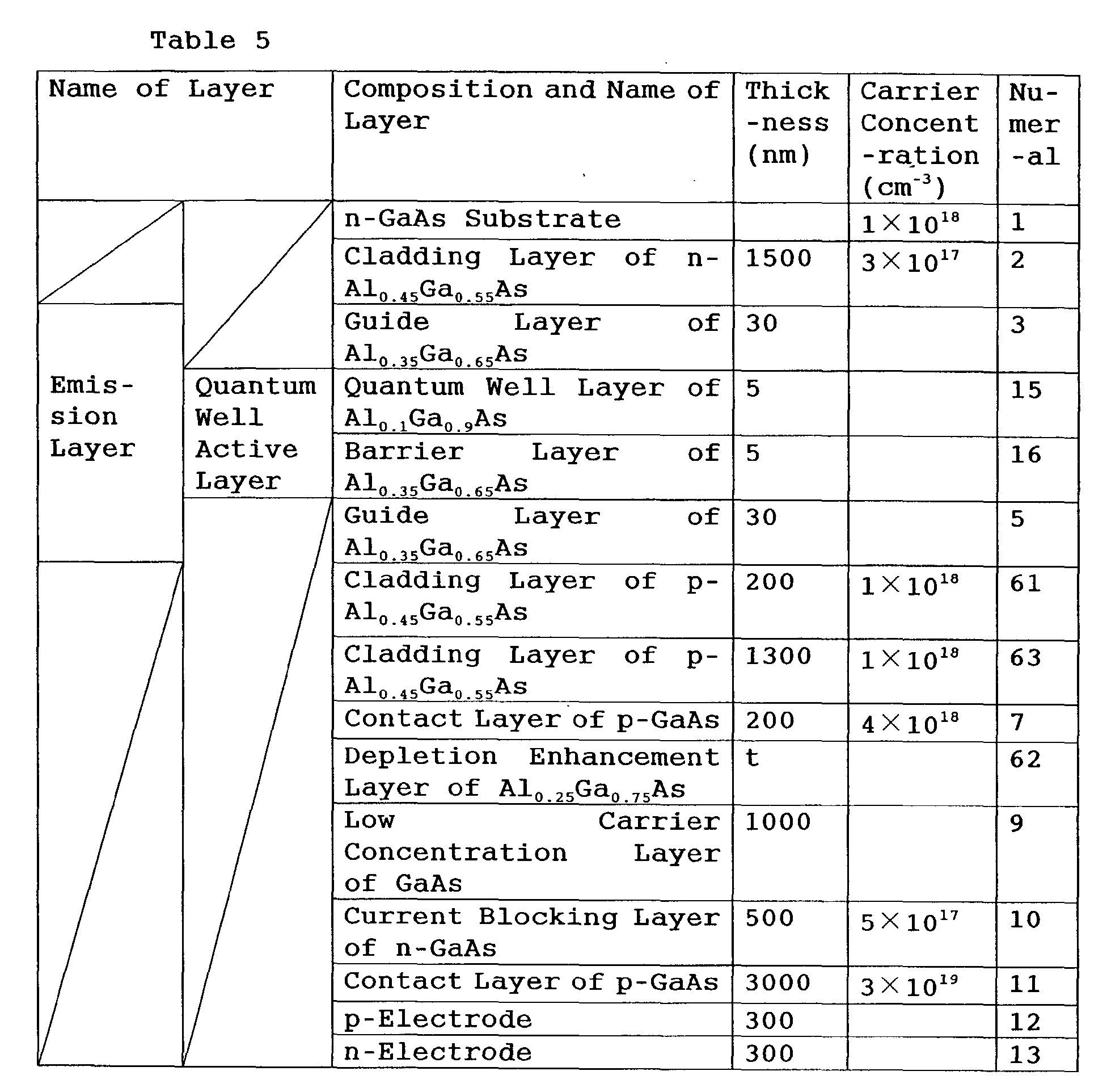


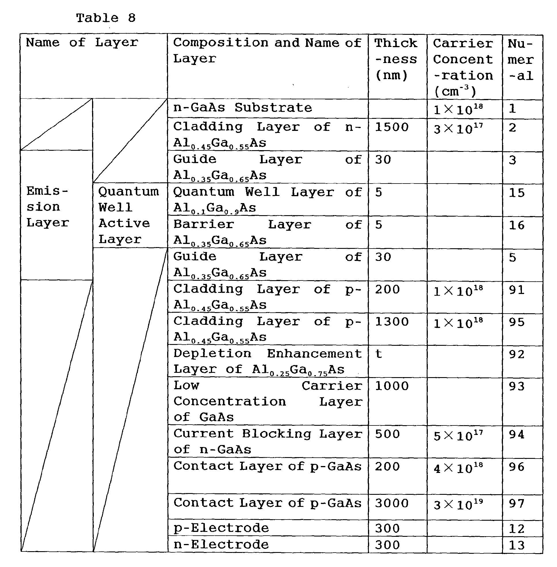
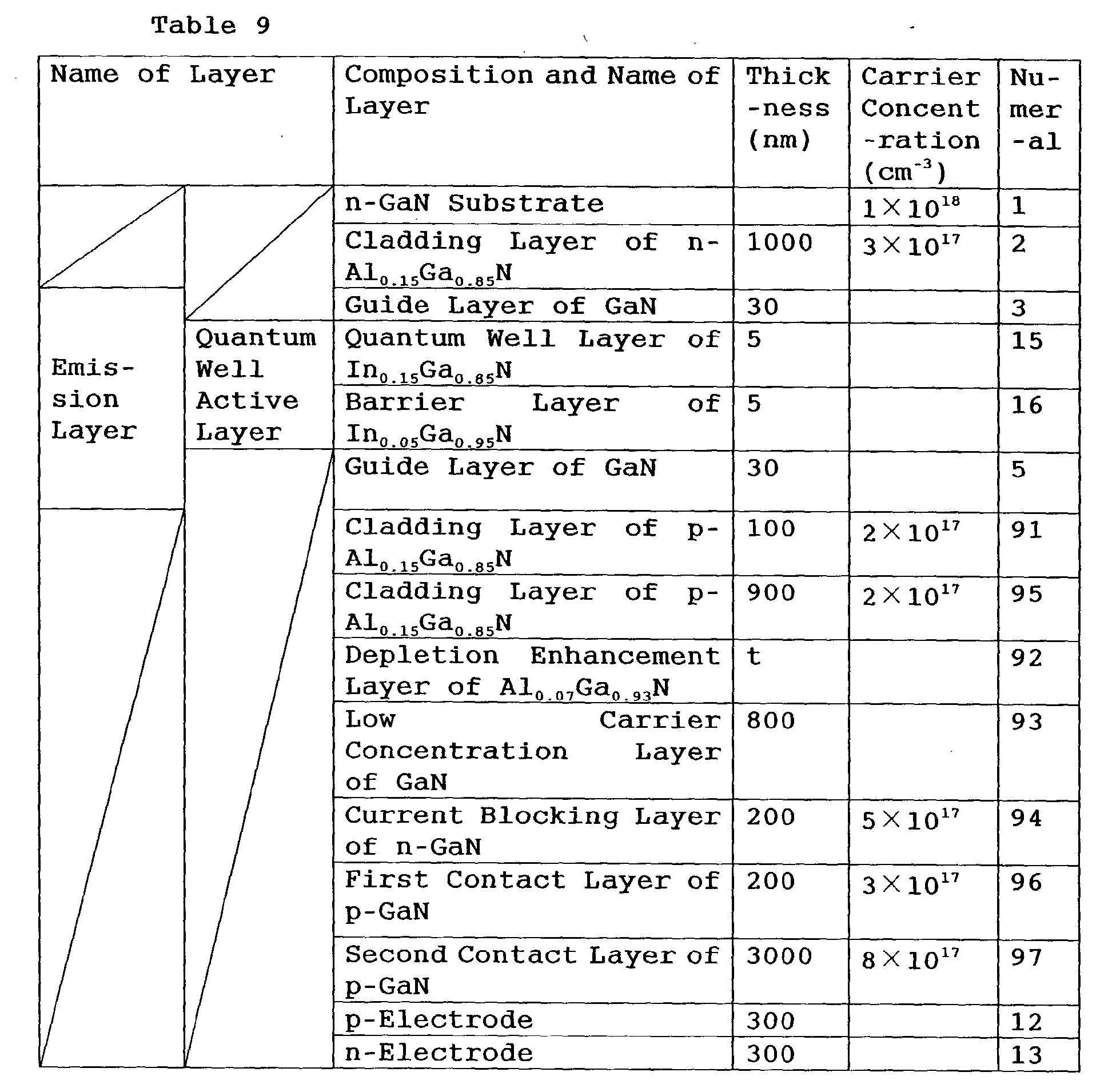

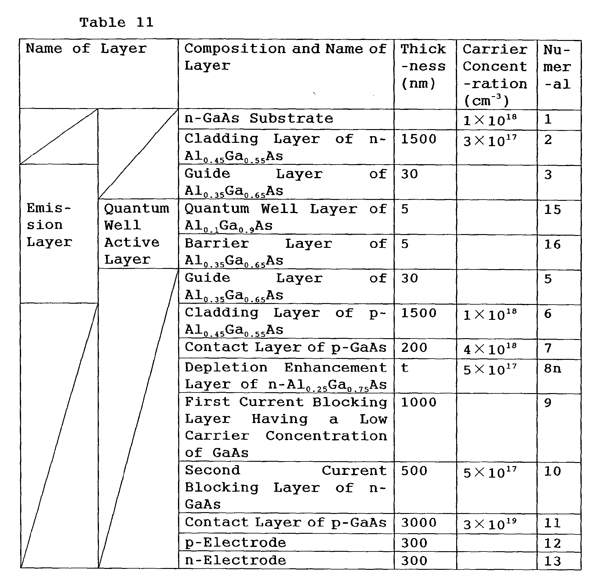
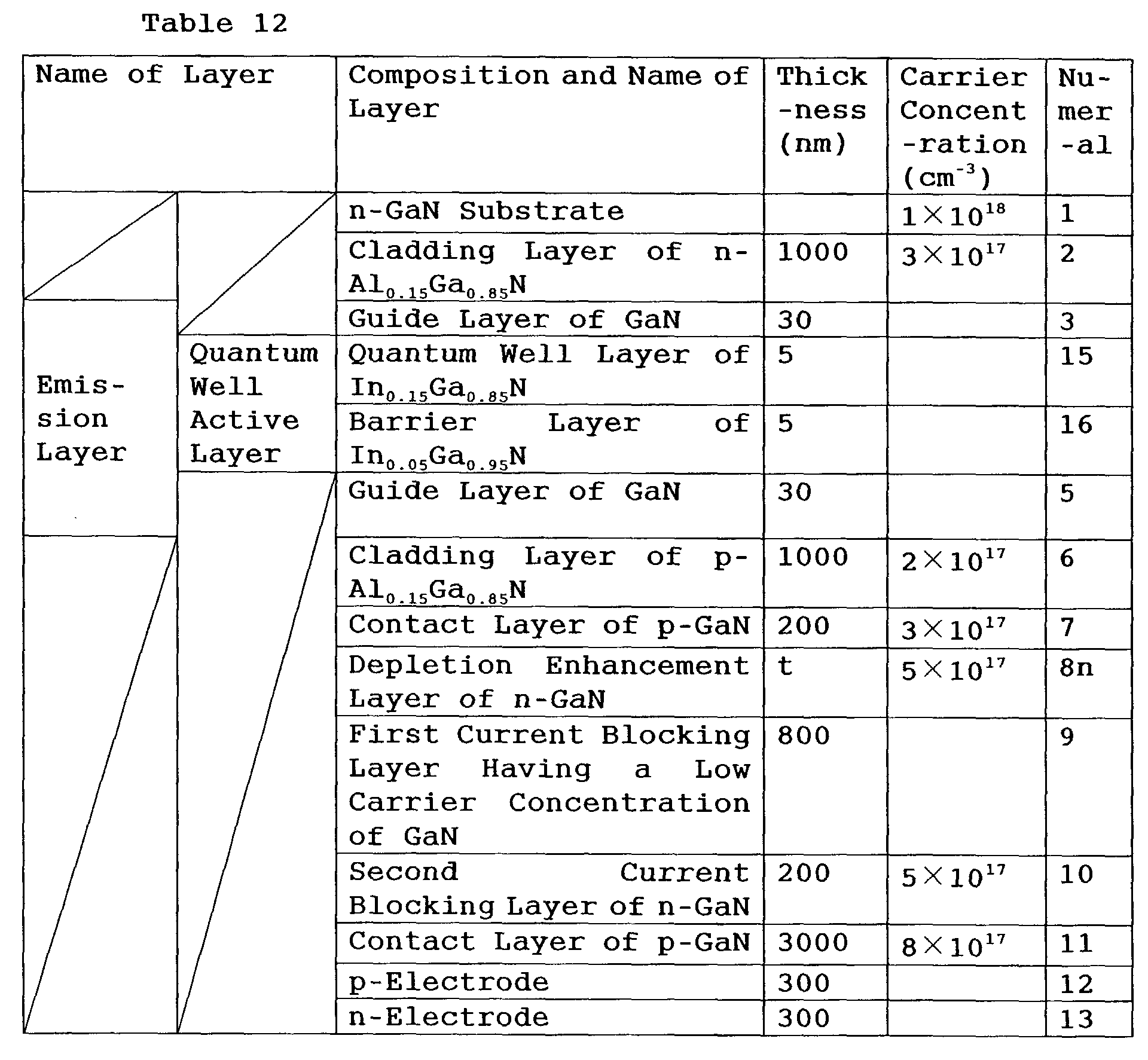

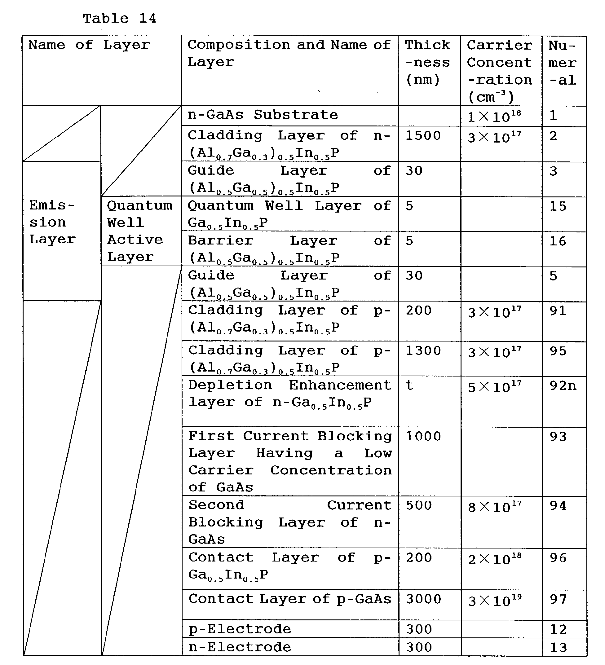
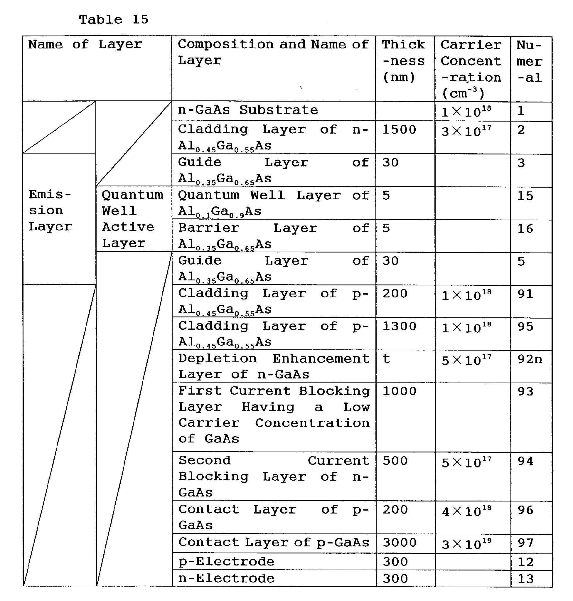

Claims (33)
- A semiconductor laser device comprising:an active layer;a first cladding layer of a first conduction type provided on said active layer;a current blocking layer of a second conduction type provided on said first cladding layer except a current injection region;a low carrier concentration layer provided on the side of said current blocking layer between said first cladding layer and said current blocking layer and having a lower carrier concentration than said current blocking layer; anda depletion enhancement layer provided on the side of said first cladding layer between said first cladding layer and said current blocking layer for inhibiting storage of carriers in said low carrier concentration layer.
- The semiconductor laser device according to claim 1, wherein
the band gaps of said first cladding layer, said depletion enhancement layer and said low carrier concentration layer are reduced in this order. - The semiconductor laser device according to claim 1, whereinsaid first cladding layer has a flat portion formed on said active layer and a ridge portion formed on said flat portion in said current injection region,said depletion enhancement layer is formed on said flat portion located on both sides of said ridge portion and on the side surfaces of said ridge portion, andsaid low carrier concentration layer and said current blocking layer are successively formed on said depletion enhancement layer.
- The semiconductor laser device according to claim 3, wherein
the thickness of said depletion enhancement layer is at least 10 nm. - The semiconductor laser device according to claim 4, wherein
the thickness of said depletion enhancement layer is at least 15 nm. - The semiconductor laser device according to claim 1, further comprising a ridge-shaped second cladding layer of a first conduction type provided on said depletion enhancement layer in said current injection region, whereinsaid depletion enhancement layer is formed on said first cladding layer, andsaid lower carrier concentration layer and said current blocking layer are successively formed on said depletion enhancement layer located on both sides of said second cladding layer and on the side surfaces of said second cladding layer.
- The semiconductor laser device according to claim 1, whereinsaid depletion enhancement layer, said low carrier concentration layer and said current blocking layer are successively formed on said first cladding layer except said current injection region,said semiconductor laser device further comprising a second cladding layer of a first conduction type provided to fill up a space enclosed with the side surfaces of said depletion enhancement layer, said low carrier concentration layer and said current blocking layer and the upper surface of said first cladding layer in said current injection region.
- The semiconductor laser device according to claim 6, wherein
the thickness of said depletion enhancement layer is at least 15 nm. - The semiconductor laser device according to claim 8, wherein
the thickness of said depletion enhancement layer is at least 20 nm. - The semiconductor laser device according to claim 7, wherein
the thickness of said depletion enhancement layer is at least 15 nm. - The semiconductor laser device according to claim 10, wherein
the thickness of said depletion enhancement layer is at least 20 nm. - The semiconductor laser device according to claim 1, wherein
said depletion enhancement layer has a single-layer structure or a superlattice structure. - The semiconductor laser device according to claim 1, whereinsaid active layer includes a layer made of (Alx1Ga1- x1)y1In1-y1P,said depletion enhancement layer is made of (Alx2Ga1- x2)y2In1-y2P or Alx2Ga1-x2As,said low carrier concentration layer is made of (Alx3Ga1-x3)y3In1-y3P or Alx3Ga1-x3As,said current blocking layer is made of (Alx4Ga1-x4)y4In1-y4P or Alx4Ga1-x4As, andsaid x1, said x2, said x3, said x4, said y1, said y2, said y3 and said y4 are at least zero and not more than 1 respectively.
- The semiconductor laser device according to claim 1, whereinsaid active layer includes a layer made of Alx1Ga1-x1As,said depletion enhancement layer is made of Alx2Ga1-x2As,said low carrier concentration layer is made of Alx3Ga1-x3As,said current blocking layer is made of Alx4Ga1-x4As, andsaid x1, said x2, said x3 and said x4 are at least zero and not more than 1 respectively.
- The semiconductor laser device according to claim 1, whereinsaid active layer is made of Inx1Ga1-x1N,said depletion enhancement layer is made of Alx2Ga1-x2N,said low carrier concentration layer is made of Alx3Ga1-x3N,said current blocking layer is made of Alx4Ga1-x4N, andsaid x1, said x2, said x3 and said x4 are at least zero and not more than 1 respectively.
- The semiconductor laser device according to claim 1, whereinsaid active layer includes a layer made of (Alx1Ga1- x1)y1In1-y1P,said depletion enhancement layer is made of (Alx2Ga1- x2)y2In1-y2P ,said low carrier concentration layer is made of Alx3Ga1-x3As,said current blocking layer is made of Alx4Ga1-x4As,said x1, said x2, said x3, said x4, said y1 and said y2 are at least zero and not more than 1 respectively, andsaid first conduction type is the p type, and said second conduction type is the n type.
- A semiconductor laser device comprising:an active layer;a first cladding layer of a first conduction type provided on said active layer;a first current blocking layer having a low carrier concentration provided on said first cladding layer except a current injection region; anda depletion enhancement layer formed between said first cladding layer and said first current blocking layer for inhibiting storage of carriers in said first current blocking layer, whereinsaid depletion enhancement layer has an energy level in band gap supplying second conduction type carriers to compensate for first conduction type carriers supplied from said first cladding layer due to a modulation doping effect.
- The semiconductor laser device according to claim 17, wherein
said first current blocking layer has a narrower band gap than said first cladding layer. - The semiconductor laser device according to claim 17, wherein
said energy level in band gap has such density that substantially all said band-to-band levels ionize under a condition applying no bias voltage. - The semiconductor laser device according to claim 17, wherein
said energy level in band gap is formed by doping with a second conduction type impurity. - The semiconductor laser device according to claim 17, wherein
the material of said depletion enhancement layer is the same as the material of said first current blocking layer. - The semiconductor laser device according to claim 17, whereinsaid first cladding layer has a larger band gap than said depletion enhancement layer,said semiconductor laser device further comprising an intermediate band gap layer provided between said first cladding layer and said depletion enhancement layer and having a band gap smaller than the band gap of said first cladding layer and larger than the band gap of said depletion enhancement layer.
- The semiconductor laser device according to claim 17, wherein
said depletion enhancement layer has a band gap smaller than the band gap of said first cladding layer and larger than the band gap of said first current blocking layer. - The semiconductor laser device according to claim 17, whereinsaid first cladding layer has a flat portion formed on said active layer and a ridge portion formed on said flat portion in said current injection region,said depletion enhancement layer is formed on-said flat portion located on both sides of said ridge portion and on the side surfaces of said ridge portion, andsaid first current blocking layer is formed on said depletion enhancement layer.
- The semiconductor laser device according to claim 17, whereinsaid depletion enhancement layer and said first current blocking layer are successively formed on said first cladding layer except said current injection region,said semiconductor laser device further comprising a second cladding layer of a first conduction type provided to fill up a space enclosed with the side surfaces of said depletion enhancement layer and said first current blocking layer and the upper surface of said first cladding layer in said current injection region.
- The semiconductor laser device according to claim 17, wherein
said depletion enhancement layer is formed on a region excluding said current injection region. - The semiconductor laser device according to claim 17, further comprising a second current blocking layer of a second conduction type provided on said first current blocking layer.
- A semiconductor laser device comprising:an active layer;a first cladding layer of a first conduction type provided on said active layer;a first current blocking layer having a low carrier concentration provided on said first cladding layer except a current injection region; anda depletion enhancement layer formed between said first cladding layer and said first current blocking layer for inhibiting storage of carriers in said first current blocking layer.
- The semiconductor laser device according to claim 28, wherein
said first current blocking layer having a low carrier concentration has a narrower band gap than said first cladding layer. - The semiconductor laser device according to claim 28, wherein
the band gaps of said first cladding layer, said depletion enhancement layer and said first current blocking layer having a low carrier concentration are reduced in this order. - The semiconductor laser device according to claim 28, whereinsaid first cladding layer has a flat portion formed on said active layer and a ridge portion formed on said flat portion in said current injection region,said depletion enhancement layer is formed on said flat portion located on both sides of said ridge portion and on the side surfaces of said ridge portion, andsaid first current blocking layer having a low carrier concentration is formed on said depletion enhancement layer.
- The semiconductor laser device according to claim 28, further comprising a ridge-shaped second cladding layer of a first conduction type provided on said depletion enhancement layer in said current injection region, whereinsaid depletion enhancement layer is formed on said first cladding layer, andsaid first current blocking layer having a lower carrier concentration is formed on said depletion enhancement layer located on both sides of said second cladding layer and on the side surfaces of said second cladding layer.
- The semiconductor laser device according to claim 28, whereinsaid depletion enhancement layer and said first current blocking layer having a low carrier concentration are successively formed on said first cladding layer except said current injection region,said semiconductor laser device further comprising a second cladding layer of a first conduction type provided to fill up a space enclosed with the side surfaces of said depletion enhancement layer and said first current blocking layer having a low carrier concentration and the upper surface of said first cladding layer in said current injection region.
Applications Claiming Priority (4)
| Application Number | Priority Date | Filing Date | Title |
|---|---|---|---|
| JP37449799 | 1999-12-28 | ||
| JP37449799A JP2001189528A (en) | 1999-12-28 | 1999-12-28 | Semiconductor laser device |
| JP2000092303 | 2000-03-29 | ||
| JP2000092303A JP3561676B2 (en) | 2000-03-29 | 2000-03-29 | Semiconductor laser device |
Publications (3)
| Publication Number | Publication Date |
|---|---|
| EP1130722A2 true EP1130722A2 (en) | 2001-09-05 |
| EP1130722A3 EP1130722A3 (en) | 2005-02-09 |
| EP1130722B1 EP1130722B1 (en) | 2007-02-14 |
Family
ID=26582593
Family Applications (1)
| Application Number | Title | Priority Date | Filing Date |
|---|---|---|---|
| EP00311645A Expired - Lifetime EP1130722B1 (en) | 1999-12-28 | 2000-12-22 | Semiconductor laser device |
Country Status (5)
| Country | Link |
|---|---|
| US (1) | US6768755B2 (en) |
| EP (1) | EP1130722B1 (en) |
| KR (1) | KR100734457B1 (en) |
| CN (1) | CN1182637C (en) |
| DE (1) | DE60033369T2 (en) |
Families Citing this family (4)
| Publication number | Priority date | Publication date | Assignee | Title |
|---|---|---|---|---|
| US6836495B2 (en) * | 2003-05-07 | 2004-12-28 | Eastman Kodak Company | Vertical cavity laser including inorganic spacer layers |
| US7773650B2 (en) | 2006-12-28 | 2010-08-10 | Nichia Corporation | Nitride semiconductor laser element |
| KR101984163B1 (en) * | 2014-12-03 | 2019-05-30 | 알페스 라제르스 에스아 | Quantum Cascade Laser with Current Blocking Layers |
| JP7323783B2 (en) | 2019-07-19 | 2023-08-09 | 日亜化学工業株式会社 | Light-emitting device manufacturing method and light-emitting device |
Family Cites Families (9)
| Publication number | Priority date | Publication date | Assignee | Title |
|---|---|---|---|---|
| JP2997573B2 (en) * | 1991-02-19 | 2000-01-11 | 株式会社東芝 | Semiconductor laser device |
| JP2914833B2 (en) * | 1992-09-14 | 1999-07-05 | シャープ株式会社 | Semiconductor laser |
| JPH08222801A (en) | 1995-02-17 | 1996-08-30 | Mitsubishi Electric Corp | Semiconductor laser |
| JPH0983071A (en) * | 1995-09-08 | 1997-03-28 | Rohm Co Ltd | Semiconductor laser |
| US5963572A (en) * | 1995-12-28 | 1999-10-05 | Sanyo Electric Co., Ltd. | Semiconductor laser device and manufacturing method thereof |
| JP3429407B2 (en) * | 1996-01-19 | 2003-07-22 | シャープ株式会社 | Semiconductor laser device and method of manufacturing the same |
| TW342545B (en) | 1996-03-28 | 1998-10-11 | Sanyo Electric Co | Semiconductor laser element and method for designing same |
| EP0828324B1 (en) * | 1996-09-06 | 2003-06-25 | Sanyo Electric Co. Ltd | Semiconductor laser device |
| US6181723B1 (en) * | 1997-05-07 | 2001-01-30 | Sharp Kabushiki Kaisha | Semiconductor light emitting device with both carbon and group II element atoms as p-type dopants and method for producing the same |
-
2000
- 2000-12-22 EP EP00311645A patent/EP1130722B1/en not_active Expired - Lifetime
- 2000-12-22 DE DE60033369T patent/DE60033369T2/en not_active Expired - Lifetime
- 2000-12-26 US US09/746,065 patent/US6768755B2/en not_active Expired - Fee Related
- 2000-12-27 KR KR1020000082568A patent/KR100734457B1/en not_active Expired - Fee Related
- 2000-12-28 CN CNB001377221A patent/CN1182637C/en not_active Expired - Fee Related
Also Published As
| Publication number | Publication date |
|---|---|
| EP1130722B1 (en) | 2007-02-14 |
| US6768755B2 (en) | 2004-07-27 |
| DE60033369D1 (en) | 2007-03-29 |
| KR100734457B1 (en) | 2007-07-03 |
| EP1130722A3 (en) | 2005-02-09 |
| CN1182637C (en) | 2004-12-29 |
| KR20010062730A (en) | 2001-07-07 |
| US20010006527A1 (en) | 2001-07-05 |
| DE60033369T2 (en) | 2007-11-29 |
| CN1302103A (en) | 2001-07-04 |
Similar Documents
| Publication | Publication Date | Title |
|---|---|---|
| US4809287A (en) | Double-heterostructure semiconductor with mesa stripe waveguide | |
| EP0616400B1 (en) | Semiconductor laser | |
| US5321712A (en) | Semiconductor light-emitting device having a cladding layer composed of an InGaAlp-based compound | |
| EP0227865B1 (en) | Light emitting semiconductor device | |
| EP0111650A2 (en) | Double-channel planar heterostructure semiconductor laser | |
| KR100271674B1 (en) | Semiconductor laser device | |
| EP0549103B1 (en) | A semiconductor laser device | |
| US5305341A (en) | Semiconductor laser whose active layer has an ordered structure | |
| US5574741A (en) | Semiconductor laser with superlattice cladding layer | |
| EP0536757B1 (en) | Semiconductor laser | |
| EP1130722B1 (en) | Semiconductor laser device | |
| US6078602A (en) | Separate confinement heterostructured semiconductor laser device having high speed characteristics | |
| JPH0786678A (en) | Semiconductor laser device | |
| US6411637B1 (en) | Semiconductor laser and method of manufacturing the same | |
| US5170404A (en) | Semiconductor laser device suitable for optical communications systems drive | |
| US6350629B1 (en) | Optical semiconductor device having active layer and carrier recombination layer different from each other | |
| JP3403915B2 (en) | Semiconductor laser | |
| JP2748570B2 (en) | Semiconductor laser device | |
| EP0867949B1 (en) | Semiconductor light-emitting device | |
| JP3561676B2 (en) | Semiconductor laser device | |
| JPH0669589A (en) | Semiconductor laser element | |
| JPH01184972A (en) | Semiconductor laser device | |
| US7208774B2 (en) | Semiconductor optical device | |
| JP2555984B2 (en) | Semiconductor laser and manufacturing method thereof | |
| JPS63133587A (en) | Buried structure semiconductor laser |
Legal Events
| Date | Code | Title | Description |
|---|---|---|---|
| PUAI | Public reference made under article 153(3) epc to a published international application that has entered the european phase |
Free format text: ORIGINAL CODE: 0009012 |
|
| AK | Designated contracting states |
Kind code of ref document: A2 Designated state(s): AT BE CH CY DE DK ES FI FR GB GR IE IT LI LU MC NL PT SE TR |
|
| AX | Request for extension of the european patent |
Free format text: AL;LT;LV;MK;RO;SI |
|
| PUAL | Search report despatched |
Free format text: ORIGINAL CODE: 0009013 |
|
| AK | Designated contracting states |
Kind code of ref document: A3 Designated state(s): AT BE CH CY DE DK ES FI FR GB GR IE IT LI LU MC NL PT SE TR |
|
| AX | Request for extension of the european patent |
Extension state: AL LT LV MK RO SI |
|
| 17P | Request for examination filed |
Effective date: 20050419 |
|
| AKX | Designation fees paid |
Designated state(s): DE FR GB NL |
|
| GRAP | Despatch of communication of intention to grant a patent |
Free format text: ORIGINAL CODE: EPIDOSNIGR1 |
|
| GRAS | Grant fee paid |
Free format text: ORIGINAL CODE: EPIDOSNIGR3 |
|
| GRAA | (expected) grant |
Free format text: ORIGINAL CODE: 0009210 |
|
| AK | Designated contracting states |
Kind code of ref document: B1 Designated state(s): DE FR GB NL |
|
| REG | Reference to a national code |
Ref country code: GB Ref legal event code: FG4D |
|
| REF | Corresponds to: |
Ref document number: 60033369 Country of ref document: DE Date of ref document: 20070329 Kind code of ref document: P |
|
| RIN2 | Information on inventor provided after grant (corrected) |
Inventor name: TAKEUCHI, KUNIO Inventor name: NOMURA, YASUHIKO Inventor name: HIROYAMA, RYOJI Inventor name: HATA, MASAYUKI Inventor name: INOUE, DAIJIRO |
|
| ET | Fr: translation filed | ||
| PLBE | No opposition filed within time limit |
Free format text: ORIGINAL CODE: 0009261 |
|
| STAA | Information on the status of an ep patent application or granted ep patent |
Free format text: STATUS: NO OPPOSITION FILED WITHIN TIME LIMIT |
|
| 26N | No opposition filed |
Effective date: 20071115 |
|
| PGFP | Annual fee paid to national office [announced via postgrant information from national office to epo] |
Ref country code: FR Payment date: 20081212 Year of fee payment: 9 |
|
| PGFP | Annual fee paid to national office [announced via postgrant information from national office to epo] |
Ref country code: GB Payment date: 20081217 Year of fee payment: 9 |
|
| GBPC | Gb: european patent ceased through non-payment of renewal fee |
Effective date: 20091222 |
|
| REG | Reference to a national code |
Ref country code: FR Ref legal event code: ST Effective date: 20100831 |
|
| PG25 | Lapsed in a contracting state [announced via postgrant information from national office to epo] |
Ref country code: FR Free format text: LAPSE BECAUSE OF NON-PAYMENT OF DUE FEES Effective date: 20091231 |
|
| PG25 | Lapsed in a contracting state [announced via postgrant information from national office to epo] |
Ref country code: GB Free format text: LAPSE BECAUSE OF NON-PAYMENT OF DUE FEES Effective date: 20091222 |
|
| PGFP | Annual fee paid to national office [announced via postgrant information from national office to epo] |
Ref country code: DE Payment date: 20101215 Year of fee payment: 11 |
|
| PGFP | Annual fee paid to national office [announced via postgrant information from national office to epo] |
Ref country code: NL Payment date: 20111221 Year of fee payment: 12 |
|
| REG | Reference to a national code |
Ref country code: NL Ref legal event code: V1 Effective date: 20130701 |
|
| REG | Reference to a national code |
Ref country code: DE Ref legal event code: R119 Ref document number: 60033369 Country of ref document: DE Effective date: 20130702 |
|
| PG25 | Lapsed in a contracting state [announced via postgrant information from national office to epo] |
Ref country code: NL Free format text: LAPSE BECAUSE OF NON-PAYMENT OF DUE FEES Effective date: 20130701 Ref country code: DE Free format text: LAPSE BECAUSE OF NON-PAYMENT OF DUE FEES Effective date: 20130702 |