EP1130714A2 - Laser elements having different wavelenghts formed from one semiconductor substrate - Google Patents
Laser elements having different wavelenghts formed from one semiconductor substrate Download PDFInfo
- Publication number
- EP1130714A2 EP1130714A2 EP00403634A EP00403634A EP1130714A2 EP 1130714 A2 EP1130714 A2 EP 1130714A2 EP 00403634 A EP00403634 A EP 00403634A EP 00403634 A EP00403634 A EP 00403634A EP 1130714 A2 EP1130714 A2 EP 1130714A2
- Authority
- EP
- European Patent Office
- Prior art keywords
- semiconductor laser
- diffraction grating
- laser elements
- length
- elements
- Prior art date
- Legal status (The legal status is an assumption and is not a legal conclusion. Google has not performed a legal analysis and makes no representation as to the accuracy of the status listed.)
- Withdrawn
Links
Images




















Classifications
-
- H—ELECTRICITY
- H01—ELECTRIC ELEMENTS
- H01S—DEVICES USING THE PROCESS OF LIGHT AMPLIFICATION BY STIMULATED EMISSION OF RADIATION [LASER] TO AMPLIFY OR GENERATE LIGHT; DEVICES USING STIMULATED EMISSION OF ELECTROMAGNETIC RADIATION IN WAVE RANGES OTHER THAN OPTICAL
- H01S5/00—Semiconductor lasers
- H01S5/02—Structural details or components not essential to laser action
- H01S5/026—Monolithically integrated components, e.g. waveguides, monitoring photo-detectors, drivers
-
- H—ELECTRICITY
- H01—ELECTRIC ELEMENTS
- H01S—DEVICES USING THE PROCESS OF LIGHT AMPLIFICATION BY STIMULATED EMISSION OF RADIATION [LASER] TO AMPLIFY OR GENERATE LIGHT; DEVICES USING STIMULATED EMISSION OF ELECTROMAGNETIC RADIATION IN WAVE RANGES OTHER THAN OPTICAL
- H01S5/00—Semiconductor lasers
- H01S5/02—Structural details or components not essential to laser action
-
- H—ELECTRICITY
- H01—ELECTRIC ELEMENTS
- H01S—DEVICES USING THE PROCESS OF LIGHT AMPLIFICATION BY STIMULATED EMISSION OF RADIATION [LASER] TO AMPLIFY OR GENERATE LIGHT; DEVICES USING STIMULATED EMISSION OF ELECTROMAGNETIC RADIATION IN WAVE RANGES OTHER THAN OPTICAL
- H01S5/00—Semiconductor lasers
- H01S5/10—Construction or shape of the optical resonator, e.g. extended or external cavity, coupled cavities, bent-guide, varying width, thickness or composition of the active region
- H01S5/12—Construction or shape of the optical resonator, e.g. extended or external cavity, coupled cavities, bent-guide, varying width, thickness or composition of the active region the resonator having a periodic structure, e.g. in distributed feedback [DFB] lasers
-
- H—ELECTRICITY
- H01—ELECTRIC ELEMENTS
- H01S—DEVICES USING THE PROCESS OF LIGHT AMPLIFICATION BY STIMULATED EMISSION OF RADIATION [LASER] TO AMPLIFY OR GENERATE LIGHT; DEVICES USING STIMULATED EMISSION OF ELECTROMAGNETIC RADIATION IN WAVE RANGES OTHER THAN OPTICAL
- H01S5/00—Semiconductor lasers
- H01S5/02—Structural details or components not essential to laser action
- H01S5/0201—Separation of the wafer into individual elements, e.g. by dicing, cleaving, etching or directly during growth
-
- H—ELECTRICITY
- H01—ELECTRIC ELEMENTS
- H01S—DEVICES USING THE PROCESS OF LIGHT AMPLIFICATION BY STIMULATED EMISSION OF RADIATION [LASER] TO AMPLIFY OR GENERATE LIGHT; DEVICES USING STIMULATED EMISSION OF ELECTROMAGNETIC RADIATION IN WAVE RANGES OTHER THAN OPTICAL
- H01S5/00—Semiconductor lasers
- H01S5/02—Structural details or components not essential to laser action
- H01S5/026—Monolithically integrated components, e.g. waveguides, monitoring photo-detectors, drivers
- H01S5/0265—Intensity modulators
-
- H—ELECTRICITY
- H01—ELECTRIC ELEMENTS
- H01S—DEVICES USING THE PROCESS OF LIGHT AMPLIFICATION BY STIMULATED EMISSION OF RADIATION [LASER] TO AMPLIFY OR GENERATE LIGHT; DEVICES USING STIMULATED EMISSION OF ELECTROMAGNETIC RADIATION IN WAVE RANGES OTHER THAN OPTICAL
- H01S5/00—Semiconductor lasers
- H01S5/10—Construction or shape of the optical resonator, e.g. extended or external cavity, coupled cavities, bent-guide, varying width, thickness or composition of the active region
- H01S5/1053—Comprising an active region having a varying composition or cross-section in a specific direction
-
- H—ELECTRICITY
- H01—ELECTRIC ELEMENTS
- H01S—DEVICES USING THE PROCESS OF LIGHT AMPLIFICATION BY STIMULATED EMISSION OF RADIATION [LASER] TO AMPLIFY OR GENERATE LIGHT; DEVICES USING STIMULATED EMISSION OF ELECTROMAGNETIC RADIATION IN WAVE RANGES OTHER THAN OPTICAL
- H01S5/00—Semiconductor lasers
- H01S5/10—Construction or shape of the optical resonator, e.g. extended or external cavity, coupled cavities, bent-guide, varying width, thickness or composition of the active region
- H01S5/12—Construction or shape of the optical resonator, e.g. extended or external cavity, coupled cavities, bent-guide, varying width, thickness or composition of the active region the resonator having a periodic structure, e.g. in distributed feedback [DFB] lasers
- H01S5/1203—Construction or shape of the optical resonator, e.g. extended or external cavity, coupled cavities, bent-guide, varying width, thickness or composition of the active region the resonator having a periodic structure, e.g. in distributed feedback [DFB] lasers over only a part of the length of the active region
-
- H—ELECTRICITY
- H01—ELECTRIC ELEMENTS
- H01S—DEVICES USING THE PROCESS OF LIGHT AMPLIFICATION BY STIMULATED EMISSION OF RADIATION [LASER] TO AMPLIFY OR GENERATE LIGHT; DEVICES USING STIMULATED EMISSION OF ELECTROMAGNETIC RADIATION IN WAVE RANGES OTHER THAN OPTICAL
- H01S5/00—Semiconductor lasers
- H01S5/20—Structure or shape of the semiconductor body to guide the optical wave ; Confining structures perpendicular to the optical axis, e.g. index or gain guiding, stripe geometry, broad area lasers, gain tailoring, transverse or lateral reflectors, special cladding structures, MQW barrier reflection layers
- H01S5/2054—Methods of obtaining the confinement
- H01S5/2077—Methods of obtaining the confinement using lateral bandgap control during growth, e.g. selective growth, mask induced
-
- H—ELECTRICITY
- H01—ELECTRIC ELEMENTS
- H01S—DEVICES USING THE PROCESS OF LIGHT AMPLIFICATION BY STIMULATED EMISSION OF RADIATION [LASER] TO AMPLIFY OR GENERATE LIGHT; DEVICES USING STIMULATED EMISSION OF ELECTROMAGNETIC RADIATION IN WAVE RANGES OTHER THAN OPTICAL
- H01S5/00—Semiconductor lasers
- H01S5/40—Arrangement of two or more semiconductor lasers, not provided for in groups H01S5/02 - H01S5/30
- H01S5/4025—Array arrangements, e.g. constituted by discrete laser diodes or laser bar
- H01S5/4087—Array arrangements, e.g. constituted by discrete laser diodes or laser bar emitting more than one wavelength
Definitions
- the present invention relates generally to a set of optical semiconductor devices having different wavelengths. More particularly, the present invention relates to a method of manufacturing a set of semiconductor laser elements having different oscillation wavelengths in which variation of coupling coefficients is minimized, so that uniformalization of laser oscillation thresholds, light emission efficiency and long-haul transmission characteristics and an improvement in the yield of single longitudinal mode oscillation can be attained.
- WDM optical communications system In order to cover communication demand which is increasing rapidly in recent years, a wavelength division multiplexing (WDM) optical communications system is progressing in which optical signals having different wavelengths are transmitted in one optical fiber and thereby communications capacity can be greatly increased without newly adding optical fibers.
- WDM optical communications system of course requires a plurality of light sources having different wavelengths. Therefore, there exists a great challenge in how efficiently the light sources having different wavelengths can be realized.
- the active layer optical absorption layer
- the band gap wavelength of the optical guide layer formed on the diffraction grating varies, and the film thickness of the active layer also varies.
- the bandgap wavelength of the guide layer varies, the absolute value of the refractive index on the diffraction grating varies and, therefore, the quantity of variation of periodic variation of the refractive index by the diffraction grating also varies.
- the optical confinement factor into the active layer varies and, as a result, intensity of light field in the diffraction grating area also varies.
- the quantity of variation of the periodic variation of the refractive index by the diffraction grating and light field intensity in the diffraction grating area are parameters which directly relate to the coupling coefficient ( ⁇ ). Therefore, in the method in which lasers having different wavelengths are fabricated all together but in which these both values vary, the value ( ⁇ ) varies depending on the oscillation wavelength.
- the mask width of the mask used in the selective growth is made large to make the oscillation wavelength long.
- the bandgap wavelength of the optical guide layer on the diffraction grating mentioned above also becomes long, the absolute value of the refractive index of the optical guide layer becomes large.
- the film thickness of the active layer becomes large, the optical confinement factor into the active layer becomes large and, as a result, the light field intensity in the diffraction grating area is decreased.
- the effect of item (1) functions to enlarge the coupling coefficient ( ⁇ )
- the effect of item (2) functions to decrease the coupling coefficient ( ⁇ ).
- the relationship between the oscillation wavelength (or the mask width of the selective growth) and the coupling coefficient ( ⁇ ) varies depending on an MOVPE apparatus for performing crystal growth or conditions in performing the growth.
- the coupling coefficient ⁇ is a parameter which closely relates to the oscillation threshold, the light emission efficiency, the oscillation yield of single longitudinal mode, the long-haul transmission characteristics and the like of the DFB laser. If unevenness occurs in the parameter, the yield of element is deteriorated.
- a first problem is that there occurs unevenness in the threshold current of the laser oscillation, the efficiency, the oscillation yield of single longitudinal mode.
- the second problem is that the yield of transmission characteristic when the long-haul transmission is performed varies depending on the wavelength.
- a set of semiconductor laser elements which perform single longitudinal mode oscillation by having periodically varying refractive index within the elements and which are formed together from one semiconductor substrate, the semiconductor laser elements having mutually different oscillation wavelengths, characterized in that each of the semiconductor laser elements comprises a diffraction grating, and a duty cycle of the diffraction grating varies so as to realize equal coupling coefficient.
- the duty cycle of the diffraction grating varies depending on the oscillation wavelength.
- each of the semiconductor laser elements comprises a distributed feedback (DFB) type semiconductor laser and an electro-absorption (EA) type optical modulator formed integrally.
- DFB distributed feedback
- EA electro-absorption
- the duty cycle of the diffraction grating is increased or decreased from 50%.
- a set of semiconductor laser elements which perform single longitudinal mode oscillation by having periodically varying refractive index within the elements and which are formed together from one semiconductor substrate, the semiconductor laser elements having mutually different oscillation wavelengths, characterized in that each of the semiconductor laser elements comprises a diffraction grating, and a product of a coupling coefficient and a length of area in which the diffraction grating is formed in each of the semiconductor laser elements or a product of a coupling coefficient and a length of each of the elements is substantially constant.
- the length of area in which the diffraction grating is formed or the length of the element varies depending on each of the oscillation wavelengths
- each of the semiconductor laser elements comprises a distributed feedback (DFB) type semiconductor laser and an electro-absorption (EA) type optical modulator formed integrally.
- DFB distributed feedback
- EA electro-absorption
- a method of manufacturing a set of semiconductor laser elements which perform single longitudinal mode oscillation by having periodically varying refractive index within the elements and which are formed together from one semiconductor substrate, the semiconductor laser elements having mutually different oscillation wavelengths, characterized in that the method comprises forming a diffraction grating for each of the semiconductor laser elements such that a duty cycle of the diffraction grating varies to realize equal coupling coefficient.
- the duty cycle of the diffraction grating varies depending on the oscillation wavelengths.
- the duty cycle of the diffraction grating varies depending on a width of a mask for selective growth of a laser element.
- the duty cycle of the diffraction grating varies depending on a location on the semiconductor substrate.
- the forming a diffraction grating for each of the semiconductor laser elements comprises: forming an electron beam sensitive resist film on a semiconductor substrate; patterning the electron beam sensitive resist film by electron beam exposure; and etching the semiconductor substrate by using the patterned electron beam sensitive resist film as a mask to produce the diffraction grating for each of the semiconductor laser elements; wherein the duty cycle of the diffraction grating is changed by changing an electron beam dosage in the electron beam exposure.
- a distributed feedback (DFB) type semiconductor laser and an electro-absorption (EA) type optical modulator are formed integrally.
- a method of manufacturing a set of semiconductor laser elements which perform single longitudinal mode oscillation by having periodically varying refractive index within the elements and which are formed together from one semiconductor substrate, the semiconductor laser elements having mutually different oscillation wavelengths, characterized in that the method comprises forming a diffraction grating for each of the semiconductor laser elements, wherein a length of area in which the diffraction grating is formed or a length of the element is adjusted every element such that a product of a coupling coefficient and the length of area in which the diffraction grating is formed in each of the semiconductor laser elements or a product of a coupling coefficient and the length of each of the elements becomes substantially constant.
- the length of area in which the diffraction grating is formed or the length of the element is varied depending on an oscillation wavelength of each laser element.
- the length of area in which the diffraction grating is formed or the length of the element is varied depending on a width of a mask for selective growth of a laser element.
- the length of area in which the diffraction grating is formed or the length of the element is varied depending on a location on the semiconductor substrate.
- a distributed feedback (DFB) type semiconductor laser and an electro-absorption (EA) type optical modulator are formed integrally.
- a coupling coefficient ( ⁇ ), which increases and decreases depending on the oscillation wavelength, varies depending on the duty cycle of each diffraction grating of the element having the coupling coefficient.
- the duty cycle of a diffraction grating is defined as [ ⁇ L M /(L M +L C ) ⁇ ⁇ 100] (%), where L M is a width of a peak and L C is a width of a valley of the diffraction grating.
- the coupling coefficient becomes maximum when the duty cycle of the diffraction grating is 50 %, and becomes small as the duty cycle of the diffraction grating departs from this value.
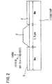
- Fig. 2 is a schematic cross sectional view of a wafer having an InGaAsP selective growth layer which is grown by the selective MOVPE method.
- an InGaAsP layer 3 By selectively growing an InGaAsP layer 3 by the MOVPE method by using a pair of SiO 2 stripe masks 2 which are formed in the direction [011] on a (100)InP substrate 1 and which have a space of 1.5 ⁇ m, an InGaAsP crystal grows into a trapezoid form whose side surface is the (111)B plane and whose top surface is the (100) plane.
- the mask width Wm is increased, the growth rate (film thickness) becomes large and indium composition increases due to the flow of raw material from top portions of the mask. By using this phenomenon, it is possible to form layer structures having different bandgap wavelengths within the same substrate surface.
- Fig. 3 is a schematic cross sectional view in the axial direction of a waveguide of a DFB laser.
- Fig. 3 shows a typical DFB laser layer structure in which a diffraction grating 100 is formed on an InP substrate 101, and, on the diffraction grating 100, an InGaAsP guide layer 104, a multi-quantum well (MQW) active layer 105 and an InP clad 106 are sequentially stacked.
- MQW multi-quantum well
- composition having a bandgap wavelength of 1.0 through 1.3 ⁇ m is preferably used in the InGaAsP guide layer 104.
- Fig. 4A shows relationships between photoluminescence wavelengths and mask widths (10-50 ⁇ m), when an InGaAsP [bandgap wavelengths 1.13 ⁇ m (Q1.13) and 1.20 ⁇ m (Q1.20)] as a guide layer on the diffraction grating of the 1.55 ⁇ m band DFB laser is grown by selective MOVPE method so as to lattice match to the InP substrate and in a condition the mask width is preferably 15 ⁇ m.
- the bandgap wavelength is 1.13 ⁇ m
- the photoluminescence wavelength increases up to 1.20 ⁇ m in length. This is because, the indium component increases due to an increase in the mask width and compressive strain is introduced.
- Fig. 4B shows an example of a relationship between photoluminescence wavelengths and mask widths (0-50 ⁇ m), when an InGaAsP/InGaAsP MQW structure is grown by selective MOVPE method.
- the mask width is set from 5 ⁇ m to 21 ⁇ m, it is possible to cover the wavelength range from 1.45 ⁇ m to 1.55 ⁇ m, which can be operating wavelengths of electro-absorption (EA) type modulators for the DFB lasers having wavelengths from 1.52 ⁇ m to 1.62 ⁇ m.
- EA electro-absorption
- the coupling coefficients ( ⁇ ) in different oscillation wavelengths.
- the bandgap wavelength of the guide layer also varies from 1.13 ⁇ m to 1.20 ⁇ m.
- an InGaAsP layer in which a bandgap wavelength becomes 1.13 ⁇ m when the mask width is 15 ⁇ m, is used as the guide layer on the diffraction grating.
- the variation of the bandgap wavelength of the guide layer means that the refractive index of the guide layer also varies. Therefore, due to the existence of the diffraction grating, the coupling coefficient ( ⁇ ) is also changed which is caused by the periodic variation of the refractive index.
- Fig. 5 shows relationships between a height of the diffraction grating, which is proportional to the quantity of variation of the periodic variation in the refractive index, and the ⁇ , obtained as a result of calculation by using guide layer composition as a parameter.
- the duty cycle of the diffraction grating ratio of the peak and the valley of the diffraction grating
- the height of the diffraction grating is 35nm, when the bandgap wavelength of the guide layer varies from 1.13 ⁇ m to 1.20 ⁇ m, it is expected that the ⁇ changes from 37.5 to 53cm -1 .
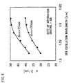
- Fig. 6 shows a result obtained by measuring the relationships between the ⁇ and the oscillation wavelengths in such DFB lasers.
- d GTG diffraction gratings
- the ⁇ varies from 30 to 40 cm -1 when the height of the diffraction grating is 30nm, and varies from 38 to 50 cm -1 when the height of the diffraction grating is 35nm.
- the quantity of variation is slightly smaller than the calculated value shown in Fig. 5. This is because, in the calculation of Fig. 5, consideration was not made on an increase in the optical confinement factor into the active layer due to an increase in the film thickness caused by an increase in the mask width.
- a carrier gas flow rate when a carrier gas flow rate is larger than that corresponding to the condition in which the uniformity of the grown film thickness within a surface becomes best, it is possible to increase the growth rate from the central portion of the substrate to the peripheral portion of the substrate (to deteriorate the uniformity).
- a carrier gas flow rate when a carrier gas flow rate is larger than that corresponding to the optimum condition for the uniformity of the grown film thickness, it is possible to realize a distribution in which the growth rate increases from the upper side to the lower side of the gas flow.
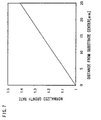
- Fig. 7 shows a normalized growth rates as a function of a distance from the center of a substrate in case the growth rate at the central portion of a 2-inch InP substrate is considered to be 1, and shows an example in which the carrier gas flow rate is set to 1.5 times the optimum condition for the uniformity, in the vertical MOVPE apparatus. It can be seen that the growth rate at the outermost periphery of the substrate is approximately 1.4 times the growth rate at the central portion of the substrate. By using this distribution of the film thickness within the surface, an InGaAsP/InGaAsP multi-quantum well structure was selectively grown.
- Fig. 8 shows a result of measurement of surface distributions of photoluminescence (PL) wavelengths thereof.
- PL photoluminescence
- Fig. 8 shows the distributions for two cases, that is, the case in which the mask width (Wm) is 6 ⁇ m and the case in which the mask width is 16 ⁇ m.
- Wm the mask width
- Fig. 8 shows the distributions for two cases, that is, the case in which the mask width (Wm) is 6 ⁇ m and the case in which the mask width is 16 ⁇ m.
- the DFB lasers having different wavelengths By utilizing these distributions, it is possible to form the DFB lasers having different wavelengths together on one semiconductor substrate.
- the mask width By setting the mask width at 16 ⁇ m, it is possible to realize the DFB lasers having a wavelength range from 1.53 ⁇ m to 1.58 ⁇ m, and, by setting the mask width at 6 ⁇ m, it is possible to realize a wavelength range from 1.46 ⁇ m to 1.51 ⁇ m, so that it is possible to obtain operation wavelengths of electro-absorption (EA) type modulator for the DFB lasers having a wavelength range from 1.53 ⁇ m to 1.58 ⁇ m.
- EA electro-absorption
- the thickness of the MQW active layers of the DFB lasers having different wavelengths in a range from 1.53 ⁇ m to 1.58 ⁇ m varies 1.4 times at maximum. Therefore, the optical confinement factor into the MQW active layer becomes larger as the thickness of the layer becomes larger in an element having longer wavelength, so that optical field in the diffraction grating portion becomes weaker. As a result, the ⁇ becomes smaller in an element having a longer wavelength.
- Fig. 9 shows a result of the actual measurement of the ⁇ .
- the depth of the diffraction grating was 35nm, and the duty cycle of the diffraction grating was 50 percent.
- the ⁇ of the element having an oscillation wavelength 1.58 ⁇ m decreases approximately to a half of that of an element having an oscillation wavelength 1.53 ⁇ m.
- the variation of the ⁇ causes problems of deterioration of the yield of single longitudinal mode oscillation and deterioration of long-haul transmission characteristic.
- the long-haul transmission characteristic is very important, because it is an item of final evaluation after fabricating the elements.
- a factor that the ⁇ affects the deterioration of the long-haul transmission characteristic is caused by a wavelength chirp induced by reflected return light in a modulation operation. Therefore, in order to enlarge the reflection immunity to suppress the wavelength chirp, it is preferable that the ⁇ is made as large as possible.
- Fig. 10 shows a relationship between the ⁇ and power penalty (shown by a dotted line and ⁇ ), and a relationship between the ⁇ and yield of single longitudinal mode oscillation (shown by a solid line and ⁇ ), with 2.5Gb/s modulation and after the transmission of 600km.
- the element used for the measurement comprises a uniform diffraction grating type DFB laser having 400 ⁇ m in length, and an EA modulator having 200 ⁇ m in length, which are monolithically integrated.
- the power penalty after the transmission of 600km becomes smaller as the ⁇ becomes larger, and when ⁇ > 37cm -1 , the power penalty equal to or smaller than 1dB is realized.
- the ⁇ becomes large, the yield of single longitudinal mode oscillation is deteriorated due to the influence of the spatial hole burning effect. Therefore, it becomes very important to control the ⁇ within a predetermined range.
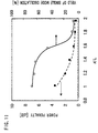
- Fig. 11 shows similar relationships as functions of the products ( ⁇ L) of the coupling coefficient and the length (L) of the DFB laser resonator. From Fig. 11, it can be seen that, in order to realize the power penalty equal to or smaller than 1dB, it is necessary that the ⁇ L is equal to or larger than 1.5.
- Fig. 12 and Fig. 13 show a relationship between the duty cycle of the diffraction grating and the ⁇ and a relationship between the duty cycle of the diffraction grating and the ⁇ L, respectively. It can be seen that each of the ⁇ and the ⁇ L becomes maximum when the duty cycle of the diffraction grating is 50 percent (when the ratio between the peak width and the valley width is 1:1). This is because, the quantity of variation of refractive index which varies due to the existence of the diffraction grating becomes maximum when the duty cycle of the diffraction grating is 50 percent.
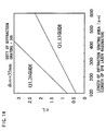
- a method in which the ⁇ is kept constant by modulating the duty cycle of the diffraction grating According to the prior art manufacturing method, the ⁇ varies depending on the oscillation wavelength. Also, as shown in Fig. 14, when the ⁇ is constant, the ⁇ L is proportional to the length L of the area where the diffraction grating is formed (the length of the laser resonator). Therefore, by adjusting the length L of the area where the diffraction grating is formed so as to cancel the variation of the ⁇ , it is possible to keep the value of the ⁇ L constant. This is the second characteristic feature of the present invention.
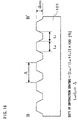
- FIG. 15A an electron beam exposure resist layer 102 is applied onto an InP substrate 101. Thereafter, an electron beam is irradiated at a period of the diffraction grating as shown in Fig. 15B and developed as shown in Fig. 15C. Then, opening portions of the resist are etched by chemical etching which uses etchant of HBr:H 2 O 2 system to form a diffraction grating structure as shown in Fig. 15D. When the resist portions are removed, the diffraction grating as shown in Fig. 16 is fabricated.
- the duty cycle of a diffraction grating is defined as [ ⁇ L M /L M +L C ) ⁇ ⁇ 100] (%), where L M is a width of a peak and L C is a width of a valley of the diffraction grating.
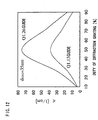
- Fig. 17 shows a relationship between the quantity of irradiation of the electron beam (electron dosage) and duty cycle of the diffraction grating obtained by experiment. As apparent from the drawing, when the electron dosage is increased, each exposure area in Fig.
- a (100)n-InP substrate 101 As shown in the drawing, positive resist 102 having electron beam sensitivity is applied on a (100)n-InP substrate 101. Then, patterns shown in Fig. 18A are written by an electron beam exposure method. Thereafter, the n-InP substrate 101 is etched by using the resist 102 as a mask and by using etching solution of HBr:H 2 O 2 system. Thereby, a diffraction grating as shown in Fig. 18B is fabricated.
- Fig. 16 corresponds to a cross sectional view taken along a line B-B' of Fig. 18B.
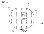
- the diffraction gratings are formed in patterns in which diffraction grating formed areas each having 800 ⁇ m in length and unformed areas each having 400 ⁇ m in length between the diffraction gratings are repeated in [011] direction, and in patterns in which diffraction gratings are repeatedly formed at a pitch of 300 ⁇ m in [01-1] direction.
- pitches of the diffraction gratings were changed from 235.05 to 250.85nm as shown in Fig.
- the duty cycles of the diffraction gratings were changed in a range from 50% to 35%, or from 50% to 67%, as shown in Figs. 21A and 21B, according to the oscillation wavelength of the DFB laser, or the mask width in the selective growth as described below.
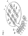
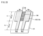
- a pair of SiO 2 stripe masks 103 for the selective MOVPE growth are patterned so as to synchronize with the diffraction gratings 100.
- Mask widths were set to W LD in each area where the diffraction grating was formed, and to W MOD in each area where the diffraction grating was not formed.
- Fig. 23 represents the SiO 2 mask patterns for only one element. That is, an area A1 having the mask width W LD (having a length of 400 ⁇ m) corresponds to a portion which becomes a DFB laser, and an area A2 having the mask width W MOD (having a length of 200 ⁇ m) corresponds to a portion which becomes an EA modulator. In this structure, the space between a pair of stripe masks had a fixed value of 1.5 ⁇ m.
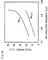
- Fig. 24 shows design values for W LD and W MOD with respect to the DFB oscillation wavelengths.
- Fig. 20, Figs. 21A and 21B and Fig. 24 show the pitches ⁇ of the diffraction gratings, the duty cycles of the diffraction gratings, W LD and W MOD , respectively, as continuous values with respect to the DFB oscillation wavelengths.
- the values in the graphs of Fig. 20, Figs. 21A and 21B and Fig. 24 have discontinuous values having 125 steps.
- a range of the DFB oscillation wavelengths from 1.52 to 1.62 ⁇ m is divided into 125 kinds of wavelengths having a space of 100GHz (approximately, a space of 0.8nm) therebetween.
- a laser active layer and a modulator absorption layer were grown thereon by the selective MOVPE growth, as shown in Fig. 25.
- Fig. 26 is a cross sectional view taken along line A-A' of Fig. 25, and shows a structure in which a dif
- Fig. 27A through 27C wherein Fig. 27A is a cross sectional view taken along line C-C' of Fig. 25, SiO 2 portions on both sides of the selective growth layer are partially removed (Fig. 27B), and, as shown in Fig.
- each portion having a total length of 600 ⁇ m including the DFB laser portion having a length of 400 ⁇ m and the EA modulator portion having a length of 200 ⁇ m was cut out.
- a high reflectance film having a reflectance of 95% was coated on the end facet on the DFB laser side, and an anti-reflective film having a reflectance equal to or lower than 0.1% was coated on the end facet on the modulator side. Evaluation of the obtained elements was done to obtain element characteristics.
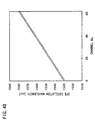
- Fig. 29 shows oscillation wavelengths of 125 elements of the fabricated DFB lasers in order. It was confirmed that the wavelength becomes longer from channel 1 to channel 125 at a slope of 0.8nm/channel which is approximately similar to the designed value, and that elements having different wavelengths covering a range from 1520 to 1620nm (from 1.52 to 1.62 ⁇ m) are realized on one substrate. Then, the ⁇ was evaluated for the elements having different DFB oscillation wavelengths. As a result, as shown in Fig. 30, it was confirmed that the ⁇ was kept approximately at the designed value of 37.5cm -1 and did not depend on the oscillation wavelength.
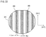
- diffraction gratings are formed by using an electron beam exposure method and by etching on a (100)n-InP substrate 201.
- the diffraction gratings 200 are formed in whole areas along [011] direction, and formed in patterns in which diffraction gratings are repeatedly formed at a pitch of 300 ⁇ m in [01-1] direction.
- pitches ⁇ of the diffraction gratings were changed from 235.05 to 250.85nm as shown in Fig.
- the duty cycles of the diffraction gratings were changed in a range from 50% to 35%, or from 50% to 67%, as shown in Figs. 21A and 21B, according to the oscillation wavelength of the DFB laser, or the mask width in the selective growth as described below.
- quantity of etching was controlled such that the height of the diffraction gratings becomes 30nm, in an etching process corresponding to that shown in Fig. 15D.
- a pair of SiO 2 stripe masks 203 for the selective MOVPE growth are formed on both sides of the diffraction gratings 200 by patterning.
- a mask width was set to W LD .
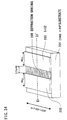
- Fig. 34 represents the SiO 2 mask patterns for only one element.
- the space between a pair of stripe masks had a fixed value of 1.5 ⁇ m.
- the design values for W LD with respect to the DFB oscillation wavelengths were the same as those of the first embodiment shown in Fig. 24.
- the values in the graphs of Fig. 20, Figs. 21A and 21B and Fig. 24 have discontinuous values having 125 steps. This is because, in the present embodiment, a range of the DFB oscillation wavelengths from 1.52 to 1.62 ⁇ m is divided into 125 kinds of wavelengths having a space of 100GHz (approximately, a space of 0.8nm) therebetween.
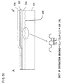
- Fig. 35A shows a cross section taken along line D-D' in Fig. 34
- a strained MQW layer (5 cycles of well layers: InGaAsP (strain of +0.60%, thickness of 10nm), and barrier layers: InGaAsP (having bandgap wavelength of 1.20 ⁇ m, thickness of 9nm))
- the height of the diffraction gratings after the selective MOVPE growth is 30nm.
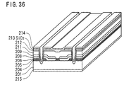
- Fig. 35C an SiO 2 mask 207 is grown on the selective growth layer, and thereafter, as shown in Fig. 35D, a p-InP block layer 208, an n-InP block layer 209, and p-InP layer 210 are selectively grown. Finally, after removing the SiO 2 mask 207, a p-InP cladding layer 211 and a p + -InGaAs cap layer 212 are formed by the selective MOVPE growth.
- Fig. 35D through Fig. 35E are described in detail in IEEE JOURNAL OF QUANTUM ELECTRONICS, Vol. 35, No. 3, pp. 368-376. Thereafter, as shown in Fig.
- patterning of p-electrode 214 is performed by using the SiO 2 film 213 as an interlayer film. Further, a back surface polishing is performed until the thickness of the n-InP substrate 201 becomes 100 ⁇ m, and an n-type electrode 215 is formed. Then, each portion having a length of 400 ⁇ m was cut out as an element. A high reflectance film having a reflectance of 95 % was coated on the back end facet of the DFB laser, and an anti-reflective film having a reflectance equal to or lower than 0.1% was coated on the front end facet thereof. Evaluation of the obtained elements was done to obtain element characteristics.
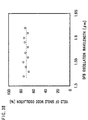
- Fig. 29 shows oscillation wavelengths of 125 elements of the fabricated DFB lasers in order. It was confirmed that the wavelength becomes longer from channel 1 to channel 125 at a slope of 0.8nm/channel which is approximately similar to the designed value, and that elements having different wavelengths covering a range from 1520 to 1620nm (from 1.52 to 1.62 ⁇ m) are realized on one substrate. Then, the ⁇ was evaluated for the elements having different DFB oscillation wavelengths. As a result, as shown in Fig. 37, it was confirmed that the coupling coefficient was kept approximately at the designed value of 30.0cm -1 and did not depend on the oscillation wavelength.
- a positive resist 102 having electron beam sensitivity is applied on a (100)n-InP substrate 101.
- patterns shown in Fig. 18A are written by an electron beam exposure method.
- the n-InP substrate 101 is etched by using the resist 102 as a mask and by using etching solution of HBr:H 2 O 2 system.
- a diffraction grating as shown in Fig. 18B is fabricated.
- Fig. 16 corresponds to a cross sectional view taken along a line B-B' of Fig. 18B.
- the diffraction gratings are formed in patterns in which diffraction grating formed areas each having 800 ⁇ m in length and unformed areas each having 400 ⁇ m in length between the diffraction gratings are repeated in [011] direction, and in patterns in which diffraction gratings are repeatedly formed at a pitch of 300 ⁇ m in [01-1] direction.
- pitches ⁇ of the diffraction gratings were changed from 236.60 to 244.65nm and, as shown in Fig. 20, the DFB oscillation wavelengths from 1.53 ⁇ m to 1.58 ⁇ m were obtained.
- the duty cycles of the diffraction gratings were changed in a range from 75% to 50%, or from 30% to 50%, as shown in Figs. 39A and 39B, according to the oscillation wavelength of the DFB laser, or according to the distance from the center of a semiconductor substrate, as described below.
- a pair of SiO 2 stripe masks for the selective MOVPE growth are patterned so as to synchronize with the diffraction gratings 100.
- Mask widths are set to W LD in each area where the diffraction grating is formed, and to W MOD in each area where the diffraction grating is not formed.
- Fig. 23 represents the SiO 2 mask patterns for only one element. That is, an area A1 having the mask width W LD (having a length of 400 ⁇ m) corresponds to a portion which becomes a DFB laser, and an area A2 having the mask width W MOD (having a length of 200 ⁇ m) corresponds to a portion which becomes an EA modulator.
- the space between a pair of stripe masks had a fixed value of 1.5 ⁇ m.
- W LD was 16 ⁇ m
- W MOD was a constant value of 6 ⁇ m.
- Fig. 20, Figs. 39A and Fig. 39B show the pitches ⁇ of the diffraction gratings and the duty cycles of the diffraction gratings, respectively, as continuous values with respect to the DFB oscillation wavelengths.
- the values in the graphs of Fig. 20, Fig. 39A and Fig. 39B have discontinuous values having 62 steps. This is because, in the present embodiment, a range of the DFB oscillation wavelengths from 1.53 to 1.58 ⁇ m is divided into 62 kinds of wavelengths having a space of 100GHz (approximately, a space of 0.8nm) therebetween.
- a laser active layer and a modulator absorption layer were grown thereon by the selective MOVPE growth, as shown in Fig. 25.
- a vertical reactor was used, and a condition was adopted such that a distribution of grown film thickness as shown in Fig. 7 was obtained by adjusting carrier gas flow rate.
- Fig. 26 is a cross sectional view taken along line A-A' of Fig. 25, and shows a structure in which a diffraction grating exists in an area of a DFB laser.
- Fig. 27 which includes cross sectional views taken along line C-C' of Fig. 25, SiO 2 portions on both sides of the selective growth layer are partially removed (Fig. 27(b)), and, as shown in Fig.
- patterning of p-electrode 110 is performed by using the SiO 2 film 109 as an interlayer film.
- each portion having a total length of 600 ⁇ m including the DFB laser portion 400 having a length of 400 ⁇ m and the EA modulator portion having a length of 200 ⁇ m was cut out.
- a high reflectance film having a reflectance of 95% was coated on the end facet on the DFB laser side, and an anti-reflective film having a reflectance equal to or lower than 0.1% was coated on the end facet on the modulator side. Evaluation of the obtained elements was done to obtain element characteristics.
- Fig. 40 shows oscillation wavelengths of 62 elements of the fabricated DFB lasers in order. It was confirmed that the wavelength becomes longer from channel 1 to channel 62 at a slope of 0.8nm/channel which is approximately similar to the designed value, and that elements having different wavelengths covering a range from 1530 to 1580nm (from 1.53 to 1.58 ⁇ m) are realized on one substrate. Then, the ⁇ was evaluated for the elements having different DFB oscillation wavelengths. As a result, as shown in Fig. 41, it was confirmed that the ⁇ was kept approximately at the designed value of 37.5cm -1 and did not depend on the oscillation wavelength.
- a method of manufacturing integrated EA modulator type DFB lasers having different wavelengths together which are different from those of the first and third embodiments, as a fourth embodiment.
- positive resist 102 having electron beam sensitivity is applied on a (100)n-InP substrate 101.
- patterns shown in Fig. 18A are written by an electron beam exposure method.
- the n-InP substrate 101 is etched by using the resist 102 as a mask and by using etching solution of HBr:H 2 O 2 system.
- a diffraction grating as shown in Fig. 18B was fabricated.
- Fig. 16 corresponds to a cross sectional view taken along a line B-B' of Fig. 18B.
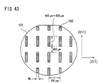
- the diffraction gratings are formed in patterns in which diffraction grating formed areas each having 400-800 ⁇ m in length and unformed areas each having 400 ⁇ m in length between the diffraction gratings are repeated in [011] direction, and in patterns in which diffraction gratings are repeatedly formed at a pitch of 300 ⁇ m in [01-1] direction.
- the diffraction grating formed area was changed according to the mask width for the selective growth of the DFB laser portion or the oscillation wavelength of the DFB laser.
- pitches ⁇ of the diffraction gratings were changed from 235.05 to 250.85nm as shown in Fig. 20, and the duty cycle of the diffraction gratings was a constant value of 50%.
- a pair of SiO 2 stripe masks 103 for the selective MOVPE growth were patterned so as to synchronize with the diffraction gratings 100.
- Mask widths were set to W LD in each area where the diffraction grating was formed, and to W MOD in each area where the diffraction grating was not formed.
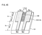
- Fig. 45 represents the SiO 2 mask patterns for only one element. That is, an area B1 having the mask width W LD (having a length of 200-400 ⁇ m) corresponds to a portion which becomes a DFB laser, and an area B2 having the mask width W MOD (having a length of 200 ⁇ m) corresponds to a portion which becomes an EA modulator. In this structure, the space between a pair of stripe masks had a fixed value of 1.5 ⁇ m.
- Fig. 24 shows design values for W LD and W MOD with respect to the DFB oscillation wavelengths.
- Fig. 20, Fig. 44A, Fig. 44B and Fig. 24 show the pitches ⁇ of the diffraction gratings, the lengths of the diffraction grating formed areas, W LD and W MOD , respectively, as continuous values with respect to the DFB oscillation wavelengths.
- the values in the graphs of Fig. 20, Fig. 44A, Fig. 44B and Fig. 24 have discontinuous values having 125 steps. This is because, in the present embodiment, a range of the DFB oscillation wavelengths from 1.52 to 1.62 ⁇ m is divided into 125 kinds of wavelengths having a space of 100GHz (approximately, a space of 0.8nm) therebetween.
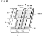
- a laser active layer and a modulator absorption layer were grown thereon by the selective MOVPE growth, as shown in Fig. 46.
- Fig. 26 is a cross sectional view taken along line A-A' of Fig. 46, and shows a structure in which a
- Fig. 26 is a cross sectional view taken along line A-A' of Fig. 46, and shows a structure in which a diffraction grating exists in an area of a DFB laser.
- Figs. 27A through 27C wherein Fig. 27A is a cross sectional view taken along line C-C' of Fig. 46, SiO 2 portions on both sides of the selective growth layer are partially removed (Fig. 27B), and, as shown in Fig.
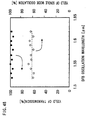
- Fig. 29 shows oscillation wavelengths of 125 elements of the fabricated DFB lasers in order. It was confirmed that the wavelength becomes longer from channel 1 to channel 125 at a slope of 0.8nm/channel which is approximately similar to the designed value, and that elements having different wavelengths covering a range from 1520 to 1620nm (from 1.52 to 1.62 ⁇ m) are realized on one substrate. Then, the ⁇ L was evaluated for the elements having different DFB oscillation wavelengths. As a result, as shown in Fig. 47, it was confirmed that the ⁇ L was kept approximately at the designed value of 1.5 and did not depend on the oscillation wavelength.
- a method of manufacturing an optical semiconductor device when DFB lasers having different wavelengths or EA modulator integrated lasers having different wavelengths are fabricated together by using a selective MOVPE method, duty cycles of diffraction gratings are increased or decreased from 50 %, depending on oscillation wavelengths, widths of dielectric masks used for selective growth, or locations on a semiconductor substrate. Thereby, coupling coefficients are maintained approximately constant, or products of the coupling coefficients and lengths of area of forming diffraction gratings or lengths of elements are maintained substantially constant.
Landscapes
- Physics & Mathematics (AREA)
- Condensed Matter Physics & Semiconductors (AREA)
- General Physics & Mathematics (AREA)
- Electromagnetism (AREA)
- Optics & Photonics (AREA)
- Semiconductor Lasers (AREA)
Abstract
Description

Claims (18)
- A set of semiconductor laser elements which perform single longitudinal mode oscillation by having periodically varying refractive index within said elements and which are formed together from one semiconductor substrate, said semiconductor laser elements having mutually different oscillation wavelengths, characterized in that each of said semiconductor laser elements comprises a diffraction grating, and a duty cycle of said diffraction grating varies so as to realize equal coupling coefficient.
- A set of semiconductor laser elements as set forth in claim 1, wherein said duty cycle of said diffraction grating varies depending on said oscillation wavelength.
- A set of semiconductor laser elements as set forth in claim 1, wherein each of said semiconductor laser elements comprises a distributed feedback (DFB) type semiconductor laser and an electro-absorption (EA) type optical modulator formed integrally.
- A set of semiconductor laser elements as set forth in claim 1, wherein said duty cycle of said diffraction grating is increased or decreased from 50%.
- A set of semiconductor laser elements which perform single longitudinal mode oscillation by having periodically varying refractive index within said elements and which are formed together from one semiconductor substrate, said semiconductor laser elements having mutually different oscillation wavelengths, characterized in that each of said semiconductor laser elements comprises a diffraction grating, and a product of a coupling coefficient and a length of area in which said diffraction grating is formed in each of said semiconductor laser elements or a product of a coupling coefficient and a length of each of said elements is substantially constant.
- A set of semiconductor laser elements as set forth in claim 5, wherein said length of area in which said diffraction grating is formed or said length of said element varies depending on each of said oscillation wavelengths
- A set of semiconductor laser elements as set forth in claim 5, wherein each of said semiconductor laser elements comprises a distributed feedback (DFB) type semiconductor laser and an electro-absorption (EA) type optical modulator formed integrally.
- A method of manufacturing a set of semiconductor laser elements which perform single longitudinal mode oscillation by having periodically varying refractive index within said elements and which are formed together from one semiconductor substrate, said semiconductor laser elements having mutually different oscillation wavelengths, characterized in that said method comprises forming a diffraction grating for each of said semiconductor laser elements such that a duty cycle of said diffraction grating varies to realize equal coupling coefficient.
- A method of manufacturing a set of semiconductor laser elements as set forth in claim 8, wherein said duty cycle of said diffraction grating varies depending on said oscillation wavelengths.
- A method of manufacturing a set of semiconductor laser elements as set forth in claim 8, wherein said duty cycle of said diffraction grating varies depending on a width of a mask for selective growth of a laser element.
- A method of manufacturing a set of semiconductor laser elements as set forth in claim 8, wherein said duty cycle of said diffraction grating varies depending on a location on said semiconductor substrate.
- A method of manufacturing a set of semiconductor laser elements as set forth in claim 8, wherein said forming a diffraction grating for each of said semiconductor laser elements comprises:forming an electron beam sensitive resist film on a semiconductor substrate;patterning said electron beam sensitive resist film by electron beam exposure; andetching said semiconductor substrate by using said patterned electron beam sensitive resist film as a mask to produce said diffraction grating for each of said semiconductor laser elements;wherein said duty cycle of said diffraction grating is changed by changing an electron beam dosage in said electron beam exposure.
- A method of manufacturing a set of semiconductor laser elements as set forth in claim 8, wherein, in each of said semiconductor laser elements, a distributed feedback (DFB) type semiconductor laser and an electro-absorption (EA) type optical modulator are formed integrally.
- A method of manufacturing a set of semiconductor laser elements which perform single longitudinal mode oscillation by having periodically varying refractive index within said elements and which are formed together from one semiconductor substrate, said semiconductor laser elements having mutually different oscillation wavelengths, characterized in that said method comprises forming a diffraction grating for each of said semiconductor laser elements, wherein a length of area in which said diffraction grating is formed or a length of said element is adjusted every element such that a product of a coupling coefficient and said length of area in which said diffraction grating is formed in each of said semiconductor laser elements or a product of a coupling coefficient and said length of each of said elements becomes substantially constant.
- A method of manufacturing a set of semiconductor laser elements as set forth in claim 14, wherein said length of area in which said diffraction grating is formed or said length of said element is varied depending on an oscillation wavelength of each laser element.
- A method of manufacturing a set of semiconductor laser elements as set forth in claim 14, wherein said length of area in which said diffraction grating is formed or said length of said element is varied depending on a width of a mask for selective growth of a laser element.
- A method of manufacturing a set of semiconductor laser elements as set forth in claim 14, wherein said length of area in which said diffraction grating is formed or said length of said element is varied depending on a location on said semiconductor substrate.
- A method of manufacturing a set of semiconductor laser elements as set forth in claim 14, wherein, in each of said semiconductor laser elements, a distributed feedback (DFB) type semiconductor laser and an electro-absorption (EA) type optical modulator are formed integrally.
Applications Claiming Priority (2)
| Application Number | Priority Date | Filing Date | Title |
|---|---|---|---|
| JP37347899A JP3307905B2 (en) | 1999-12-28 | 1999-12-28 | Optical semiconductor device and method of manufacturing the same |
| JP37347899 | 1999-12-28 |
Publications (2)
| Publication Number | Publication Date |
|---|---|
| EP1130714A2 true EP1130714A2 (en) | 2001-09-05 |
| EP1130714A3 EP1130714A3 (en) | 2004-03-03 |
Family
ID=18502234
Family Applications (1)
| Application Number | Title | Priority Date | Filing Date |
|---|---|---|---|
| EP00403634A Withdrawn EP1130714A3 (en) | 1999-12-28 | 2000-12-21 | Laser elements having different wavelenghts formed from one semiconductor substrate |
Country Status (3)
| Country | Link |
|---|---|
| US (2) | US20010005391A1 (en) |
| EP (1) | EP1130714A3 (en) |
| JP (1) | JP3307905B2 (en) |
Families Citing this family (10)
| Publication number | Priority date | Publication date | Assignee | Title |
|---|---|---|---|---|
| JP3847038B2 (en) | 1999-11-26 | 2006-11-15 | Necエレクトロニクス株式会社 | Optical semiconductor device and manufacturing method thereof |
| JP2001320124A (en) * | 2000-05-09 | 2001-11-16 | Nec Corp | Modulator integrated light source and module for optical communication |
| JP2003023209A (en) * | 2001-07-06 | 2003-01-24 | Furukawa Electric Co Ltd:The | Semiconductor device manufacturing method and semiconductor device |
| GB2378311A (en) * | 2001-08-03 | 2003-02-05 | Marconi Caswell Ltd | Tunable Laser |
| JP4552894B2 (en) * | 2006-05-12 | 2010-09-29 | 住友電気工業株式会社 | Method for fabricating distributed feedback semiconductor laser |
| KR20130080937A (en) * | 2012-01-06 | 2013-07-16 | 삼성전자주식회사 | Apparatus and method for dislplaying a screen of portable device having a flexible display |
| JP6291849B2 (en) * | 2014-01-10 | 2018-03-14 | 三菱電機株式会社 | Semiconductor device manufacturing method, semiconductor device |
| US11133649B2 (en) * | 2019-06-21 | 2021-09-28 | Palo Alto Research Center Incorporated | Index and gain coupled distributed feedback laser |
| CN114545700A (en) * | 2020-11-24 | 2022-05-27 | 华星光通科技股份有限公司 | Optical communication element with multiple sets of gratings |
| WO2023012925A1 (en) * | 2021-08-04 | 2023-02-09 | 日本電信電話株式会社 | Semiconductor optical device and method for producing same |
Family Cites Families (6)
| Publication number | Priority date | Publication date | Assignee | Title |
|---|---|---|---|---|
| JPH05110187A (en) * | 1991-10-15 | 1993-04-30 | Matsushita Electric Ind Co Ltd | Array type semiconductor laser and manufacturing method thereof |
| JPH05136521A (en) * | 1991-11-13 | 1993-06-01 | Fujitsu Ltd | Semiconductor laser |
| JPH0613701A (en) * | 1992-06-25 | 1994-01-21 | Fujitsu Ltd | Semiconductor laser manufacturing method |
| JP3611593B2 (en) * | 1994-02-14 | 2005-01-19 | 日本オプネクスト株式会社 | Method for fabricating semiconductor optical device |
| JPH10117040A (en) * | 1996-10-08 | 1998-05-06 | Nec Corp | Semiconductor laser device and method of manufacturing the same |
| EP0952470A3 (en) * | 1998-04-23 | 2004-01-14 | Nec Corporation | A method of manufacturing a semiconductor optical waveguide array and an array-structured semiconductor optical device |
-
1999
- 1999-12-28 JP JP37347899A patent/JP3307905B2/en not_active Expired - Fee Related
-
2000
- 2000-12-19 US US09/741,303 patent/US20010005391A1/en not_active Abandoned
- 2000-12-21 EP EP00403634A patent/EP1130714A3/en not_active Withdrawn
-
2002
- 2002-03-12 US US10/095,960 patent/US20020101897A1/en not_active Abandoned
Also Published As
| Publication number | Publication date |
|---|---|
| EP1130714A3 (en) | 2004-03-03 |
| US20020101897A1 (en) | 2002-08-01 |
| JP3307905B2 (en) | 2002-07-29 |
| US20010005391A1 (en) | 2001-06-28 |
| JP2001189522A (en) | 2001-07-10 |
Similar Documents
| Publication | Publication Date | Title |
|---|---|---|
| JP4643794B2 (en) | Semiconductor light emitting device | |
| US5436195A (en) | Method of fabricating an integrated semiconductor light modulator and laser | |
| JP3339488B2 (en) | Optical semiconductor device and method of manufacturing the same | |
| EP0706243A2 (en) | Distributed feedback semiconductor laser and method for producing the same | |
| EP1073169A1 (en) | Distributed feedback type semiconductor laser device having gradually-changed coupling coefficient | |
| JP2982422B2 (en) | Semiconductor laser and method of manufacturing the same | |
| EP0661783B1 (en) | Method for fabricating semiconductor light integrated circuit | |
| EP1104060B1 (en) | Optical semiconductor device and process for producing the same | |
| EP1130714A2 (en) | Laser elements having different wavelenghts formed from one semiconductor substrate | |
| JP2701569B2 (en) | Method for manufacturing optical semiconductor device | |
| EP0793280B1 (en) | An edge emitting LED and method of forming the same | |
| EP0753914B1 (en) | Laser diode element with excellent intermodulation distortion characteristic | |
| JP2763090B2 (en) | Semiconductor laser device, manufacturing method thereof, and crystal growth method | |
| Okai et al. | Complex-coupled/spl lambda//4-shifted DFB lasers with a flat FM response | |
| GB2292011A (en) | Semiconductor optical devices and methods for fabrication | |
| JP2002057405A (en) | Semiconductor laser device and method of manufacturing the same | |
| JPH06283802A (en) | Semiconductor laser device and fabrication thereof | |
| JP4115593B2 (en) | Gain-coupled distributed feedback semiconductor laser device and manufacturing method thereof | |
| CA2210008C (en) | Laser diode element with excellent intermodulation distortion characteristic | |
| JP2669045B2 (en) | Manufacturing method of distributed feedback semiconductor laser | |
| JP2914235B2 (en) | Semiconductor optical device and method of manufacturing the same | |
| JPH07335977A (en) | Semiconductor laser, optical integrated device, and manufacturing method thereof | |
| JP3228235B2 (en) | Method for manufacturing semiconductor optical waveguide structure |
Legal Events
| Date | Code | Title | Description |
|---|---|---|---|
| PUAI | Public reference made under article 153(3) epc to a published international application that has entered the european phase |
Free format text: ORIGINAL CODE: 0009012 |
|
| AK | Designated contracting states |
Kind code of ref document: A2 Designated state(s): AT BE CH CY DE DK ES FI FR GB GR IE IT LI LU MC NL PT SE TR |
|
| AX | Request for extension of the european patent |
Free format text: AL;LT;LV;MK;RO;SI |
|
| RAP1 | Party data changed (applicant data changed or rights of an application transferred) |
Owner name: NEC COMPOUND SEMICONDUCTOR DEVICES, LTD. |
|
| PUAL | Search report despatched |
Free format text: ORIGINAL CODE: 0009013 |
|
| AK | Designated contracting states |
Kind code of ref document: A3 Designated state(s): AT BE CH CY DE DK ES FI FR GB GR IE IT LI LU MC NL PT SE TR |
|
| AX | Request for extension of the european patent |
Extension state: AL LT LV MK RO SI |
|
| RIC1 | Information provided on ipc code assigned before grant |
Ipc: 7H 01S 5/40 B Ipc: 7H 01S 5/026 B Ipc: 7H 01S 5/02 B Ipc: 7H 01S 5/12 A |
|
| 17P | Request for examination filed |
Effective date: 20040512 |
|
| AKX | Designation fees paid |
Designated state(s): FR IT |
|
| REG | Reference to a national code |
Ref country code: DE Ref legal event code: 8566 |
|
| 17Q | First examination report despatched |
Effective date: 20050203 |
|
| STAA | Information on the status of an ep patent application or granted ep patent |
Free format text: STATUS: THE APPLICATION IS DEEMED TO BE WITHDRAWN |
|
| 18D | Application deemed to be withdrawn |
Effective date: 20050614 |