EP1130467A2 - Photo mask pattern designing method, resist pattern fabricating method and semiconductor device manufacturing method - Google Patents
Photo mask pattern designing method, resist pattern fabricating method and semiconductor device manufacturing method Download PDFInfo
- Publication number
- EP1130467A2 EP1130467A2 EP01400471A EP01400471A EP1130467A2 EP 1130467 A2 EP1130467 A2 EP 1130467A2 EP 01400471 A EP01400471 A EP 01400471A EP 01400471 A EP01400471 A EP 01400471A EP 1130467 A2 EP1130467 A2 EP 1130467A2
- Authority
- EP
- European Patent Office
- Prior art keywords
- photo mask
- pattern
- mask
- exposure
- region
- Prior art date
- Legal status (The legal status is an assumption and is not a legal conclusion. Google has not performed a legal analysis and makes no representation as to the accuracy of the status listed.)
- Withdrawn
Links
Images





Classifications
-
- G—PHYSICS
- G03—PHOTOGRAPHY; CINEMATOGRAPHY; ANALOGOUS TECHNIQUES USING WAVES OTHER THAN OPTICAL WAVES; ELECTROGRAPHY; HOLOGRAPHY
- G03F—PHOTOMECHANICAL PRODUCTION OF TEXTURED OR PATTERNED SURFACES, e.g. FOR PRINTING, FOR PROCESSING OF SEMICONDUCTOR DEVICES; MATERIALS THEREFOR; ORIGINALS THEREFOR; APPARATUS SPECIALLY ADAPTED THEREFOR
- G03F7/00—Photomechanical, e.g. photolithographic, production of textured or patterned surfaces, e.g. printing surfaces; Materials therefor, e.g. comprising photoresists; Apparatus specially adapted therefor
- G03F7/70—Microphotolithographic exposure; Apparatus therefor
- G03F7/70425—Imaging strategies, e.g. for increasing throughput or resolution, printing product fields larger than the image field or compensating lithography- or non-lithography errors, e.g. proximity correction, mix-and-match, stitching or double patterning
- G03F7/70466—Multiple exposures, e.g. combination of fine and coarse exposures, double patterning or multiple exposures for printing a single feature
-
- H—ELECTRICITY
- H10—SEMICONDUCTOR DEVICES; ELECTRIC SOLID-STATE DEVICES NOT OTHERWISE PROVIDED FOR
- H10P—GENERIC PROCESSES OR APPARATUS FOR THE MANUFACTURE OR TREATMENT OF DEVICES COVERED BY CLASS H10
- H10P76/00—Manufacture or treatment of masks on semiconductor bodies, e.g. by lithography or photolithography
-
- G—PHYSICS
- G03—PHOTOGRAPHY; CINEMATOGRAPHY; ANALOGOUS TECHNIQUES USING WAVES OTHER THAN OPTICAL WAVES; ELECTROGRAPHY; HOLOGRAPHY
- G03F—PHOTOMECHANICAL PRODUCTION OF TEXTURED OR PATTERNED SURFACES, e.g. FOR PRINTING, FOR PROCESSING OF SEMICONDUCTOR DEVICES; MATERIALS THEREFOR; ORIGINALS THEREFOR; APPARATUS SPECIALLY ADAPTED THEREFOR
- G03F1/00—Originals for photomechanical production of textured or patterned surfaces, e.g., masks, photo-masks, reticles; Mask blanks or pellicles therefor; Containers specially adapted therefor; Preparation thereof
- G03F1/26—Phase shift masks [PSM]; PSM blanks; Preparation thereof
-
- G—PHYSICS
- G03—PHOTOGRAPHY; CINEMATOGRAPHY; ANALOGOUS TECHNIQUES USING WAVES OTHER THAN OPTICAL WAVES; ELECTROGRAPHY; HOLOGRAPHY
- G03F—PHOTOMECHANICAL PRODUCTION OF TEXTURED OR PATTERNED SURFACES, e.g. FOR PRINTING, FOR PROCESSING OF SEMICONDUCTOR DEVICES; MATERIALS THEREFOR; ORIGINALS THEREFOR; APPARATUS SPECIALLY ADAPTED THEREFOR
- G03F1/00—Originals for photomechanical production of textured or patterned surfaces, e.g., masks, photo-masks, reticles; Mask blanks or pellicles therefor; Containers specially adapted therefor; Preparation thereof
- G03F1/26—Phase shift masks [PSM]; PSM blanks; Preparation thereof
- G03F1/30—Alternating PSM, e.g. Levenson-Shibuya PSM; Preparation thereof
-
- G—PHYSICS
- G03—PHOTOGRAPHY; CINEMATOGRAPHY; ANALOGOUS TECHNIQUES USING WAVES OTHER THAN OPTICAL WAVES; ELECTROGRAPHY; HOLOGRAPHY
- G03F—PHOTOMECHANICAL PRODUCTION OF TEXTURED OR PATTERNED SURFACES, e.g. FOR PRINTING, FOR PROCESSING OF SEMICONDUCTOR DEVICES; MATERIALS THEREFOR; ORIGINALS THEREFOR; APPARATUS SPECIALLY ADAPTED THEREFOR
- G03F1/00—Originals for photomechanical production of textured or patterned surfaces, e.g., masks, photo-masks, reticles; Mask blanks or pellicles therefor; Containers specially adapted therefor; Preparation thereof
- G03F1/68—Preparation processes not covered by groups G03F1/20 - G03F1/50
- G03F1/70—Adapting basic layout or design of masks to lithographic process requirements, e.g., second iteration correction of mask patterns for imaging
-
- G—PHYSICS
- G03—PHOTOGRAPHY; CINEMATOGRAPHY; ANALOGOUS TECHNIQUES USING WAVES OTHER THAN OPTICAL WAVES; ELECTROGRAPHY; HOLOGRAPHY
- G03F—PHOTOMECHANICAL PRODUCTION OF TEXTURED OR PATTERNED SURFACES, e.g. FOR PRINTING, FOR PROCESSING OF SEMICONDUCTOR DEVICES; MATERIALS THEREFOR; ORIGINALS THEREFOR; APPARATUS SPECIALLY ADAPTED THEREFOR
- G03F7/00—Photomechanical, e.g. photolithographic, production of textured or patterned surfaces, e.g. printing surfaces; Materials therefor, e.g. comprising photoresists; Apparatus specially adapted therefor
- G03F7/20—Exposure; Apparatus therefor
- G03F7/2022—Multi-step exposure, e.g. hybrid; backside exposure; blanket exposure, e.g. for image reversal; edge exposure, e.g. for edge bead removal; corrective exposure
- G03F7/203—Multi-step exposure, e.g. hybrid; backside exposure; blanket exposure, e.g. for image reversal; edge exposure, e.g. for edge bead removal; corrective exposure comprising an imagewise exposure to electromagnetic radiation or corpuscular radiation
Definitions
- This invention relates to a photo mask pattern designing method, resist pattern fabricating method and semiconductor device manufacturing method, especially suitable for application to correction of the pattern configuration of a photo mask used in a lithographic process for multiplexing exposure.
- phase shift mask has come to be used as a technique for making a micro pattern below the wavelength of light used upon exposure.
- this type of phase shift mask a high resolution can be obtained by using a phase difference of beams of light transmitting the mask. Therefore, adjacent beams of transmitted light must be inverted in phase from each other.
- phase shift mask As a technology for making a micro pattern using such a phase shift mask, there is a method which once executes exposure by using the phase shift mask, and thereafter again executes exposure for removing an undesired pattern produced by the first exposure, that is, executes twin exposure, to make a pattern.
- the twin exposure technique is under practical use for manufacturing high-speed LSI.
- phase shift mask is fabricated in a critical region of the photo mask fabricating technique. Therefore, correction for thinning the line width of the pattern on the photo mask applies a large load to fabrication of the mask.
- difference in density of patterns on a photo mask is getting larger.
- the increase of difference in density is accompanied by a tendency toward a larger amount of correction of patterns.
- a photo mask pattern designing method configured to correct pattern configuration of at least one of a plurality of kinds of photo masks used upon making a single-layered resist pattern by transferring pattern configuration through a plurality of times of exposure of a resist coated on a substrate, characterized in that:
- a resist pattern fabricating method configured to fabricate a single-layered resist pattern on a resist coated on a substrate by executing a plurality of times of exposure including first exposure using a first photo mask and interference of light and a second exposure using a second photo mask, characterized in that:
- a semiconductor device manufacturing method configured to make a resist pattern on a resist coated on a semiconductor substrate by executing a plurality of times of exposure including first exposure using a first photo mask and interference of light and second exposure using a second photo mask, and thereafter process the semiconductor substrate by using the resist pattern as a mask, characterized in that:
- correction of the second shading region of the second photo mask is preferably conducted preferentially. Further, in the present invention, correction of the first shading region includes correction by which the correction amount results in zero.
- correction of the first shading region and correction of the second shading region are conducted toward reducing the line width range in the single-layered resist pattern made by at least two exposure steps using a first photo mask and a second photo mask, respectively.
- a third translucent region is typically provided to sandwich the first shading region, and light beams transmitting the first translucent region and the third translucent region are different in phase by approximately 180°.
- the first photo mask is typically a phase shift mask.
- the phase shift mask is typically a Rebenson phase shift mask, but if necessary, a half-tone phase shift mask, an auxiliary pattern mask, edge-enhanced phase shift mask, chromeless phase shift mask, or the like, may be used.
- the second photo mask is typically a binary mask.
- the base for making a resist pattern on is a base having a 70 nm thick organic nonreflecting film, for example, formed by spin coating on a silicon (Si) substrate, for example.
- a resist coating apparatus by spin coating, for example, a chemically amplified positive resist having a thickness around 400 nm, for example, is coated on the base, and thereafter, it is pre-baked at the temperature of 110°C for 90 seconds, for example.
- twin exposure using a KrF excimer laser stepper is conducted.
- the twin exposure according to the embodiment will be explained below.
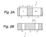
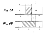
- FIGs. I and 2 illustrate an example of pattern configurations on a photo mask, assuming a gate of a DRAM-incorporated logic LSI used in the embodiment. This embodiment is explained as making a resist pattern for fabricating a gate patter of a DRAM-incorporated logic LSI having the gate length of 0.10 ⁇ m.
- Fig. 1 shows an isolated pattern for making a resist pattern with an isolated line pattern configuration having the gate length of 0.10 ⁇ m, for example, assuming a gate in a logic portion.
- the pattern configuration shown in Fig. 1A is that on a phase shift mask 1 whereas the pattern configuration shown in Fig. 1B is that on a binary mask 2.
- hatched portions are shading regions, and the other regions are translucent regions. These shading regions and translucent regions lie in corresponding locations in the phase shift mask 1 and the binary mask 2.
- the translucent region 12 and the translucent region 13 at opposite sides of the shading region (mask pattern) 11 of the phase shift mask 1 shown in Fig. 1A are configured such that beams of light transmitting them are different in phase from each other by approximately 180°.
- the width of the shading region 21 shown in Fig. 1B toward the adjacent translucent region 22 is larger than the shading region 11 of the phase shift mask 1.
- the overlapping width a 1 of the translucent region 12 of the phase shift mask 1 and the shading region 21 of the binary mask 2, the line width b 1 of the shading region 11 of the phase shift mask 1 in the direction toward the translucent region 12 adjacent to the shading region 11, and the width c 1 of the translucent region 12 in the same direction are determined to be optimum values, depending upon the lien width of an intended resist pattern. A correction method for optimizing the values will be explained later.
- Fig. 2 shows an L/S pattern for making a resist pattern having a line-and-space pattern (L/S pattern) configuration having the gate length of 0.10 ⁇ m and the gate pitch of 0.34 ⁇ m, for example, assuming a gate in a DRAM portion.
- the pattern configuration shown in Fig. 2A is that on the phase shift mask 1 whereas the pattern configuration shown in Fig. 2B is that on the binary mask 2.
- hatched portions are shading regions, and the other regions are translucent regions. They are configured such that beams of light transmitting the translucent region 15 and the translucent region 16 at opposite sides of the shading region (mask pattern) 14 shown in Fig. 2A are different in phase from each other by 180°.
- the width of the shading region 23 shown in Fig. 1B toward the adjacent translucent region 24 is larger than the shading region 14 of the phase shift mask 1.
- the overlapping width a 2 of the translucent region 16 of the phase shift mask 1 and the shading region 23 of the binary mask 2, the line width b 2 of the shading region 14 of the phase shift mask toward the translucent region 15, and the width c 2 of the translucent region 15 in the same direction are determined to be optimum values, depending upon the line width in the intended resist pattern. A correction method for optimizing these values will be explained later.
- predetermined exposure is conducted to each resist as the first exposure by fixing the numerical aperture (NA) at 0.60 and using the phase shift mask I having the pattern shown in Figs. 1A and 2A.
- the second exposure is conducted by using the binary mask 2 having the pattern shown in Fig. 1B and Fig. 2B.
- the partial coherence factor ( ⁇ ) is 0.53
- the exposure is 26 mJ/cm 2
- the focus is -0.1 ⁇ m.
- the second exposure can be executed by using deformed illumination like 1/2 zone illumination.
- post-exposure baking is conducted at the temperature of 100°C for 90 seconds, for example.
- TMAH tetramethyl ammonium hydroxide
- paddle development is conducted for 60 seconds, for example.
- post-baking processing is performed at the temperature of 100°C for 90 seconds, for example.
- the resist pattern formed on the base by the above-explained method undergoes evaluation of the isolated pattern and the L/S pattern, using an ED window made of the exposure tolerance and the depth of focus.
- This evaluation is made on a sample having the overlapping width a 1 shown in Fig. 1 being 60 nm, the line width b 1 of the shading region 11 being 130 nm, the width c 1 of the translucent region 12 being 500 nm, and overlapping width a 2 shown in Fig. 2 being 60 nm, the line width b 2 of the shading region 14 being 130 nm, and the width c 2 of the translucent region 15 being 210 nm.
- the partial coherence factor ( ⁇ ) is 0.53 like that of the second exposure, and as the line width standard, the value of 0.10 ⁇ m ⁇ 0.01 ⁇ m is the tolerance.
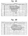
- a window obtained by that ED window evaluation is shown in Fig. 3.
- Fig. 3A shows the window in the isolated pattern whereas Fig. 3B shows the window in the L/S pattern.
- the isolated pattern and the L/S pattern are largely different in optimum exposure in the ED window of the isolated pattern shown in Fig. 3A and the ED window of the L/S pattern shown in Fig. 3B. That is, it is understood that in the ED window, the optimum exposure in the L/S pattern is larger than the optimum exposure in the isolated pattern by 19 mJ/cm 2 , and a common ED window cannot be obtained.
- correction is made to two kinds of masks, namely, the phase shift mask 1 and the binary mask 2 used in the twin exposure toward substantially equalizing their optimum exposures from the ED windows shown in Figs. 3A and 3B.
- FIG. 4 shows a flow chart of the photo mask correction method according to the embodiment.
- the pattern configuration of the single-layered resist pattern to be made is first divided into a plurality of pattern configurations having the same line width and/or the same pitch in step ST1.
- the example of the pattern configuration obtained by division in step ST1 is assumed to be the isolated pattern configuration shown in Fig. 1 (first pattern) and the L/S pattern configuration shown in Fig. 2 (second pattern).
- step ST2 optimum exposure is obtained in each of the patterns divided in step ST1 and having the same line width and the same pitch.
- the optimum exposure in the isolated pattern shown in Fig. 1 and the optimum exposure in the L/S pattern shown in Fig. 2 are obtained.
- the optimum exposure in the isolated pattern shown in Fig. 1 is 30 ⁇ 32 mJ/cm 2 as shown in the ED window of Fig. 3A
- the optimum exposure in the L/S pattern shown in Fig. 2 is 48 ⁇ 52 mJ/cm 2 as shown in the ED window of Fig. 3B. That is, the optimum exposure values in the isolated pattern and the L/S pattern obtained by step ST2 are different by 19 mJ/cm 2 .
- step ST3 correction is made to the pattern configuration of the phase shift mask 1 and the pattern configuration of the binary mask 2 to equalize the optimum exposure values of all patterns divided in step ST1.
- the pattern configurations are corrected toward decreasing the optimum exposure in the L/S pattern and increasing the optimum exposure in the isolated pattern to substantially equalize their optimum exposure values.
- Figs. 5A and 5B show dependency of the line width of the photo mask pattern upon the optimum exposure.
- Fig. 5A is a graph standardizing the optimum exposure by the optimum exposure upon a 1 being 60 nm when fixing the line width b 1 of the isolated pattern in the phase shift mask 1 shown in Fig. 1A at 130 nm and changing the overlapping width a 1 of the translucent region 13 of the phase shift mask 1 and the shading region 21 of the binary mask 2 shown in Fig. 1.
- Fig. 5B is a graph standardizing the optimum exposure by the optimum exposure upon b 1 being 130 nm when fixing the overlapping width a 1 of the translucent region 13 of the phase shift mask 1 and the shading region 21 of the binary mask 2 shown in Fig.
- the increase amount of the optimum exposure along with the increase of a 1 is smaller than the increase amount of the optimum exposure along with the increase of b 1 . This means that influences of a fabrication error of a mask with the overlapping width a 1 are larger than influences of a fabrication error of a mask with the line width b 1 .
- correction in the overlapping width a 1 should be preferred to correction in the line width b 1 .
- the line width b 1 of the pattern of the phase shift mask 1 is around the fabrication limit of a mask in most cases, and also because correction to decrease the line width b 1 is more difficult than correction to decrease the overlapping width a 1 , it is recommended to prefer correction to the overlapping width a 1 . That is, the overlapping width a 1 is corrected until the increase amount of the optimum exposure substantially converges by the graph shown in Fig. 5, and if a further increase of the optimum exposure is necessary, the line width b 1 is corrected.
- correction is made toward decreasing at least one of the overlapping width a 1 of the translucent region 13 of the phase shift mask 1 and the shading region 21 of the binary mask 2 and the line width b 1 of the pattern of the phase shift mask 1.
- step ST4 shown in Fig. 4 it is judged whether the correction amount by the correction explained below is within the fabrication limit of the phase shift mask 1 and the binary mask 2 or not.
- step ST4 If the correction amount is judged to be out of the fabrication limit in step ST4, then the flow moves to step ST3 to correct the overlapping width a 1 and the line width b 1 of the isolated pattern of the phase shift mask shown in Fig. 1 and the overlapping width a 2 and the line width b 2 of the L/S pattern of the phase shift mask shown in Fig. 2 toward equalizing their optimum exposure values.
- step ST4 the flow moves to step ST5.
- step ST5 the EP window is confirmed for the resist pattern made by using the photo mask after correction of equalizing the optimum exposure values.
- the ED window in the isolated pattern after correction is shown in Fig. 8A, and the ED window in the L/S pattern is shown in Fig. 8B.
- the optimum exposure is 40 ⁇ 44 mJ/cm 2 and the optimum focus is -0.2 ⁇ 0.2 ⁇ m.
- ((44-40)/42) 9.5% as the tolerance for exposure and 0.4 ⁇ m as the depth of focus are ensured.
- the optimum exposure is 40 ⁇ 43 mJ/cm 2 and the optimum focus is -0.3 ⁇ 0.2 ⁇ m.
- ((43-40/42) 7.2% as the tolerance for exposure and 0.5 ⁇ m as the depth of focus are ensured.
- Fig. 9 shows a common ED window extracted from the ED windows shown in Figs. 8A and 8B. It is appreciated from the common ED window 31 that in case of co-existence of an isolated pattern and an L/S pattern, the optimum exposure is 42 ⁇ 44 mJ/cm 2 and the optimum focus is -0.2 ⁇ 0.1 ⁇ m and that in case of exposure of the resist pattern including both the isolated pattern shown in Fig. 1A and the L/S pattern shown in Fig. 2A, the exposure is preferably 42 ⁇ 44 mJ/cm 2 and the focus is preferably -0.2 ⁇ 0.1 ⁇ m.
- step ST3 the phase shift mask 1 and the binary mask 2 are corrected again in the same manner as already explained.
- the invention in case of making a resist pattern by conducting exposure at least twice, since the correction amounts in the phase shift mask 1 and the binary mask 2 as determined by using ED windows after dividing the resist pattern into patterns having the same line width and/or the same pitch, it is possible to efficiently correct the photo mask used for fabricating the resist pattern including a plurality of patterns such as isolated pattern and L/S pattern, for example, thereby easily fix their line widths, and enlarge the depth of focus in exposure and the exposure tolerance upon fabricating the resist pattern.
- the line width b 2 in the shading region of the L/S pattern which will be the smallest after correction, is around 110 nm, and it is possible to amply cope with the mask fabricating technique for the generation of 0.13 ⁇ m.
- the fabrication limit is taken into account, it is possible to ensure a high resolution, sufficient exposure tolerance, depth of focus and alignment accuracy, depending upon the line width of the pattern possible to fabricate, even when the line width of the pattern possible to make in the mask is reduced. Since the exposure tolerance the depth of focus can be enlarged in this manner, the invention is readily applicable to mass production of semiconductor devices.
- numerical values indicated in the explanation of the foregoing embodiment are not but examples, and any appropriate other numerical values may be employed, if necessary.
- numerical values of a 1 , a 2 , b 1 , b 2 , c 1 and c 2 shown in the embodiment are those to be determined appropriately depending upon the line width of a target resist pattern, it is possible to employ other numerical values, taking the target resist pattern and the limit of pattern line width possible to fabricate into consideration, and the invention is not limited to the use of the said numerical values.
- etching and impurity-doping may be conducted to a conductive film and an insulating film formed on a semiconductor substrate by a known method, using that resist pattern as a mask, to manufacture the target DRAM-incorporated logic LSI through predetermined processes sequentially.
- the base for making the resist pattern according to the invention for example, it is possible to use any of various types of bases such as a base having formed wiring and a base having formed an inter-layer insulating film on a semiconductor substrate having formed a semiconductor device, for example.
- the method for fabricating the resist pattern according to the invention is applicable to all cases where a resist pattern having both a regular pattern and a random pattern has to be made.
- a photo mask pattern can be corrected, with which a resist pattern locally different in pattern density can be made accurately while ensuring a sufficient exposure tolerance and a sufficient lithographic process tolerance such as depth of focus, for example.
- a resist pattern locally different in pattern density can be made accurately while ensuring a sufficient exposure tolerance and a sufficient lithographic process tolerance such as depth of focus, for example.
- a resist pattern locally different in pattern density can be made accurately while ensuring a sufficient exposure tolerance and a sufficient lithographic process tolerance such as depth of focus, for example. Therefore, the invention is applicable to a mass-manufacturing process of semiconductor devices each having patterns different in pattern density, and even in this case, semiconductor devices with a high reliability can be manufactured.
Landscapes
- Physics & Mathematics (AREA)
- General Physics & Mathematics (AREA)
- Electromagnetism (AREA)
- Preparing Plates And Mask In Photomechanical Process (AREA)
- Exposure And Positioning Against Photoresist Photosensitive Materials (AREA)
- Exposure Of Semiconductors, Excluding Electron Or Ion Beam Exposure (AREA)
Abstract
Description
- conducting the first exposure of the first shading region by using the first photo mask corrected in width in the direction of adjacent alignment of the first shading region and the first translucent region; and
- conducting the second exposure of the second shading region by using the second photo mask corrected in width in the direction of adjacent alignment of the second shading region and the second translucent region.
- conducting the first exposure of the first shading region by using the first photo mask corrected in width in the direction of adjacent alignment of the first shading region and the first translucent region; and
- conducting the second exposure of the second shading region by using the second photo mask corrected in width in the direction of adjacent alignment of the second shading region and the second translucent region.
Claims (13)
- A photo mask pattern designing method configured to correct pattern configuration of at least one of a plurality of kinds of photo masks used upon making a single-layered resist pattern by transferring pattern configuration through a plurality of times of exposure of a resist coated on a substrate, characterized in that:a first photo mask (1) used for exposure using interference of light among said plurality of times of exposure has a first shading region (11; 14) and a first translucent region (13;16) adjacent to each other;a second photo mask (2) used for exposure before or after said exposure using interference of light has a second shading region (21;23) and a second translucent region (22;24) adjacent to each other;said first shading region and said second shading region are substantially aligned in location in said first photo mask and said second photo mask;said first translucent region and said second translucent region are substantially aligned in location in said first photo mask and said second photo mask;said first shading region is corrected in width (b1;b2) in the direction of adjacent alignment of said first shading region and said first translucent region; andsaid second shading region is corrected in width (a1;a2) in the direction of adjacent alignment of said second shading region and said second translucent region.
- The photo mask pattern designing method according to claim 1 wherein correction of said second shading region (21;23) in said second photo mask is preferentially conducted.
- The photo mask pattern designing method according to claim I wherein said first photo mask (1) is a phase shift mask.
- The photo mask pattern designing method according to claim 1 wherein said second photo mask (2) is a binary mask.
- The photo mask pattern designing method according to claim 1 wherein said pattern configuration of said single-layered resist pattern is divided into pattern configurations having substantially the same line width and substantially the same pitch.
- A resist pattern fabricating method configured to fabricate a single-layered resist pattern on a resist coated on a substrate by executing a plurality of times of exposure including first exposure using a first photo mask (1) and interference of light and a second exposure using a second photo mask (2), characterized in that:and comprising the steps of:a first shading region (11;14) formed on said first photo mask (1) and a second shading region (21;23) formed on said second photo mask (2) are substantially aligned in location on said first photo mask and said second photo mask; anda first translucent region (13;16) formed on said first photo mask and a second translucent region (22;24) formed on said second photo mask are substantially aligned in location on said first photo mask and said second photo mask,conducting said first exposure of said first shading region (11; 14) by using said first photo mask corrected in width (b1;b2) in the direction of adjacent alignment of said first shading region and said first translucent region; andconducting said second exposure of said second shading region (21;23) by using said second photo mask corrected in width (a1;a2) in the direction of adjacent alignment of said second shading region and said second translucent region.
- The resist pattern fabricating method according to claim 6 wherein correction of said second shading region (21;23) in said second photo mask is preferentially conducted.
- The resist pattern fabricating method according to claim 6 wherein said first photo mask (1) is a phase shift mask.
- The resist pattern fabricating method according to claim 6 wherein said second photo mask (2) is a binary mask.
- A semiconductor device manufacturing method configured to make a resist pattern on a resist coated on a semiconductor substrate by executing a plurality of times of exposure including first exposure using a first photo mask (1) and interference of light and second exposure using a second photo mask (2), and thereafter process said semiconductor substrate by using said resist pattern as a mask, characterized in that:and comprising the steps of:a first shading region (11;14) formed on said first photo mask and a second shading region (21;23) formed on said second photo mask are substantially aligned in location on said first photo mask and said second photo mask; anda first translucent region (13;16) formed on said first photo mask and a second translucent region (22;24) formed on said second photo mask are substantially aligned in location on said first photo mask and said second photo mask,conducting said first exposure of said first shading region (11;14) by using said first photo mask corrected in width (b1;b2) in the direction of adjacent alignment of said first shading region and said first translucent region; andconducting said second exposure of said second shading region (21;23) by using said second photo mask corrected in width (a1;a2) in the direction of adjacent alignment of said second shading region and said second translucent region.
- The semiconductor device manufacturing method according to claim 10 wherein correction of said second shading region (21;23) in said second photo mask is preferentially conducted.
- The semiconductor device manufacturing method according to claim 10 wherein said first photo mask (1) is a phase shift mask.
- The semiconductor device manufacturing method according to claim 10 wherein said second photo mask (2) is a binary mask.
Applications Claiming Priority (2)
| Application Number | Priority Date | Filing Date | Title |
|---|---|---|---|
| JP2000047605 | 2000-02-24 | ||
| JP2000047605A JP2001235850A (en) | 2000-02-24 | 2000-02-24 | Method for designing photomask pattern, method for forming resist pattern, and method for manufacturing semiconductor device |
Publications (2)
| Publication Number | Publication Date |
|---|---|
| EP1130467A2 true EP1130467A2 (en) | 2001-09-05 |
| EP1130467A3 EP1130467A3 (en) | 2001-12-05 |
Family
ID=18569829
Family Applications (1)
| Application Number | Title | Priority Date | Filing Date |
|---|---|---|---|
| EP01400471A Withdrawn EP1130467A3 (en) | 2000-02-24 | 2001-02-22 | Photo mask pattern designing method, resist pattern fabricating method and semiconductor device manufacturing method |
Country Status (7)
| Country | Link |
|---|---|
| US (1) | US6576377B2 (en) |
| EP (1) | EP1130467A3 (en) |
| JP (1) | JP2001235850A (en) |
| KR (1) | KR20010085443A (en) |
| CA (1) | CA2336569A1 (en) |
| SG (1) | SG89377A1 (en) |
| TW (1) | TW482948B (en) |
Cited By (1)
| Publication number | Priority date | Publication date | Assignee | Title |
|---|---|---|---|---|
| CN106896648A (en) * | 2013-12-30 | 2017-06-27 | 中芯国际集成电路制造(上海)有限公司 | Expose the modification method of targeted graphical |
Families Citing this family (15)
| Publication number | Priority date | Publication date | Assignee | Title |
|---|---|---|---|---|
| GB0019283D0 (en) * | 2000-08-04 | 2000-09-27 | Novartis Ag | Organic compounds |
| JP4053723B2 (en) * | 2000-09-27 | 2008-02-27 | 株式会社東芝 | Method for manufacturing exposure mask |
| JP3633506B2 (en) * | 2001-05-24 | 2005-03-30 | ソニー株式会社 | Exposure method and semiconductor device manufacturing method |
| US6721938B2 (en) * | 2001-06-08 | 2004-04-13 | Numerical Technologies, Inc. | Optical proximity correction for phase shifting photolithographic masks |
| JP3827544B2 (en) * | 2001-08-31 | 2006-09-27 | 株式会社ルネサステクノロジ | Manufacturing method of semiconductor integrated circuit device |
| JP2003121977A (en) * | 2001-10-12 | 2003-04-23 | Hitachi Ltd | Method of manufacturing semiconductor integrated circuit device and mask |
| KR20030057601A (en) * | 2001-12-29 | 2003-07-07 | 주식회사 하이닉스반도체 | Liquid crystal mask for lithography |
| EP2433871A3 (en) * | 2002-06-19 | 2012-07-11 | Medical Instill Technologies, Inc. | Sterile filling machine having needle filling station within e-beam chamber |
| JP4528558B2 (en) * | 2004-05-28 | 2010-08-18 | 株式会社東芝 | Pattern data creation method and pattern verification method |
| KR100765606B1 (en) * | 2006-10-20 | 2007-10-09 | 동부일렉트로닉스 주식회사 | Semiconductor mask pattern manufacturing method and pattern forming method using the same |
| EP2562599B1 (en) | 2009-01-29 | 2014-12-10 | Digiflex Ltd. | Process for producing a photomask on a photopolymeric surface |
| US8015512B2 (en) * | 2009-04-30 | 2011-09-06 | Macronix International Co., Ltd. | System for designing mask pattern |
| JP2010276960A (en) * | 2009-05-29 | 2010-12-09 | Toshiba Corp | Method of creating phase shift mask or mask data thereof, and method of manufacturing semiconductor device |
| KR102170143B1 (en) | 2013-08-19 | 2020-10-26 | 삼성전자주식회사 | photo-mask corrected exposure latitude err and registration err, and registration correction method of the same |
| JP7596139B2 (en) | 2020-12-21 | 2024-12-09 | 株式会社Screenホールディングス | Drawing device, drawing system, and drawing method |
Family Cites Families (8)
| Publication number | Priority date | Publication date | Assignee | Title |
|---|---|---|---|---|
| DE2835313A1 (en) | 1978-08-11 | 1980-03-13 | Siemens Ag | Structure transfer of semiconductor circuits onto glass plate - defines coarse and fine structures and exposes differently photosensitive film through both structures |
| US4456371A (en) | 1982-06-30 | 1984-06-26 | International Business Machines Corporation | Optical projection printing threshold leveling arrangement |
| US5536604A (en) * | 1992-07-17 | 1996-07-16 | Kabushiki Kaisha Toshiba | Exposure mask |
| JP3082529B2 (en) | 1993-09-13 | 2000-08-28 | 株式会社日立製作所 | Mask defect repair method |
| JPH1012543A (en) | 1996-06-20 | 1998-01-16 | Mitsubishi Electric Corp | Method of forming pattern using phase shift mask |
| JPH1032156A (en) * | 1996-07-15 | 1998-02-03 | Mitsubishi Electric Corp | Exposure apparatus and pattern forming method using phase shift mask |
| US5858580A (en) * | 1997-09-17 | 1999-01-12 | Numerical Technologies, Inc. | Phase shifting circuit manufacture method and apparatus |
| US6335128B1 (en) * | 1999-09-28 | 2002-01-01 | Nicolas Bailey Cobb | Method and apparatus for determining phase shifts and trim masks for an integrated circuit |
-
2000
- 2000-02-24 JP JP2000047605A patent/JP2001235850A/en active Pending
-
2001
- 2001-02-14 TW TW090103241A patent/TW482948B/en not_active IP Right Cessation
- 2001-02-15 CA CA002336569A patent/CA2336569A1/en not_active Abandoned
- 2001-02-15 SG SG200100806A patent/SG89377A1/en unknown
- 2001-02-16 US US09/783,973 patent/US6576377B2/en not_active Expired - Fee Related
- 2001-02-21 KR KR1020010008682A patent/KR20010085443A/en not_active Withdrawn
- 2001-02-22 EP EP01400471A patent/EP1130467A3/en not_active Withdrawn
Cited By (2)
| Publication number | Priority date | Publication date | Assignee | Title |
|---|---|---|---|---|
| CN106896648A (en) * | 2013-12-30 | 2017-06-27 | 中芯国际集成电路制造(上海)有限公司 | Expose the modification method of targeted graphical |
| CN106896648B (en) * | 2013-12-30 | 2019-01-22 | 中芯国际集成电路制造(上海)有限公司 | Correction method of exposure target pattern |
Also Published As
| Publication number | Publication date |
|---|---|
| EP1130467A3 (en) | 2001-12-05 |
| US20020006553A1 (en) | 2002-01-17 |
| SG89377A1 (en) | 2002-06-18 |
| CA2336569A1 (en) | 2001-08-24 |
| TW482948B (en) | 2002-04-11 |
| US6576377B2 (en) | 2003-06-10 |
| JP2001235850A (en) | 2001-08-31 |
| KR20010085443A (en) | 2001-09-07 |
Similar Documents
| Publication | Publication Date | Title |
|---|---|---|
| US6576377B2 (en) | Photo mask pattern designing method, resist pattern fabricating method and semiconductor device manufacturing method | |
| US7984393B2 (en) | System and method for making photomasks | |
| US20150169820A1 (en) | Weak points auto-correction process for opc tape-out | |
| US6226781B1 (en) | Modifying a design layer of an integrated circuit using overlying and underlying design layers | |
| CN114326290B (en) | Optical Proximity Correction Method | |
| US7694269B2 (en) | Method for positioning sub-resolution assist features | |
| US20010024760A1 (en) | Method of optical proximity correction | |
| US6636294B2 (en) | Microdevice and structural components of the same | |
| US8129078B2 (en) | Mask, method for manufacturing the same, and method for manufacturing semiconductor device | |
| CN1688934B (en) | Method for manufacturing semiconductor device | |
| US6420077B1 (en) | Contact hole model-based optical proximity correction method | |
| US20100073648A1 (en) | Masks and Methods of Manufacture Thereof | |
| US6187486B1 (en) | Method of multi-exposure for improving photolithography resolution | |
| JP4115615B2 (en) | Mask pattern design method | |
| US6821711B2 (en) | Manufacturing method of a phase-shift mask, method of forming a resist pattern and manufacturing method of a semiconductor device | |
| US20090125865A1 (en) | System and method for making photomasks | |
| US20100136487A1 (en) | Pattern formation method using levenson-type mask and method of manufacturing levenson-type mask | |
| US6638664B2 (en) | Optical mask correction method | |
| CN114063380A (en) | Pattern correction method and method for forming semiconductor structure | |
| CN116263560B (en) | Optical Proximity Correction Method | |
| US7294440B2 (en) | Method to selectively correct critical dimension errors in the semiconductor industry | |
| JP4691840B2 (en) | Mask pattern generation method and photomask | |
| US7297468B2 (en) | Method for forming a structure element on a wafer by means of a mask and a trimming mask assigned hereto | |
| US6316340B1 (en) | Photolithographic process for preventing corner rounding | |
| US20070178410A1 (en) | Method of forming three-dimensional lithographic pattern |
Legal Events
| Date | Code | Title | Description |
|---|---|---|---|
| PUAI | Public reference made under article 153(3) epc to a published international application that has entered the european phase |
Free format text: ORIGINAL CODE: 0009012 |
|
| AK | Designated contracting states |
Kind code of ref document: A2 Designated state(s): AT BE CH CY DE DK ES FI FR GB GR IE IT LI LU MC NL PT SE TR Kind code of ref document: A2 Designated state(s): DE FR |
|
| AX | Request for extension of the european patent |
Free format text: AL;LT;LV;MK;RO;SI |
|
| PUAL | Search report despatched |
Free format text: ORIGINAL CODE: 0009013 |
|
| AK | Designated contracting states |
Kind code of ref document: A3 Designated state(s): AT BE CH CY DE DK ES FI FR GB GR IE IT LI LU MC NL PT SE TR |
|
| AX | Request for extension of the european patent |
Free format text: AL;LT;LV;MK;RO;SI |
|
| 17P | Request for examination filed |
Effective date: 20020528 |
|
| AKX | Designation fees paid |
Free format text: DE FR |
|
| STAA | Information on the status of an ep patent application or granted ep patent |
Free format text: STATUS: THE APPLICATION HAS BEEN WITHDRAWN |
|
| 18W | Application withdrawn |
Effective date: 20060127 |