EP1130444A2 - Resistor array with position dependent heat dissipation - Google Patents
Resistor array with position dependent heat dissipation Download PDFInfo
- Publication number
- EP1130444A2 EP1130444A2 EP01300343A EP01300343A EP1130444A2 EP 1130444 A2 EP1130444 A2 EP 1130444A2 EP 01300343 A EP01300343 A EP 01300343A EP 01300343 A EP01300343 A EP 01300343A EP 1130444 A2 EP1130444 A2 EP 1130444A2
- Authority
- EP
- European Patent Office
- Prior art keywords
- heater
- thin film
- thermally conductive
- resistor array
- conductive regions
- Prior art date
- Legal status (The legal status is an assumption and is not a legal conclusion. Google has not performed a legal analysis and makes no representation as to the accuracy of the status listed.)
- Granted
Links
Images

Classifications
-
- G—PHYSICS
- G02—OPTICS
- G02F—OPTICAL DEVICES OR ARRANGEMENTS FOR THE CONTROL OF LIGHT BY MODIFICATION OF THE OPTICAL PROPERTIES OF THE MEDIA OF THE ELEMENTS INVOLVED THEREIN; NON-LINEAR OPTICS; FREQUENCY-CHANGING OF LIGHT; OPTICAL LOGIC ELEMENTS; OPTICAL ANALOGUE/DIGITAL CONVERTERS
- G02F1/00—Devices or arrangements for the control of the intensity, colour, phase, polarisation or direction of light arriving from an independent light source, e.g. switching, gating or modulating; Non-linear optics
-
- G—PHYSICS
- G02—OPTICS
- G02B—OPTICAL ELEMENTS, SYSTEMS OR APPARATUS
- G02B26/00—Optical devices or arrangements for the control of light using movable or deformable optical elements
- G02B26/004—Optical devices or arrangements for the control of light using movable or deformable optical elements based on a displacement or a deformation of a fluid
-
- B—PERFORMING OPERATIONS; TRANSPORTING
- B41—PRINTING; LINING MACHINES; TYPEWRITERS; STAMPS
- B41J—TYPEWRITERS; SELECTIVE PRINTING MECHANISMS, i.e. MECHANISMS PRINTING OTHERWISE THAN FROM A FORME; CORRECTION OF TYPOGRAPHICAL ERRORS
- B41J2/00—Typewriters or selective printing mechanisms characterised by the printing or marking process for which they are designed
- B41J2/005—Typewriters or selective printing mechanisms characterised by the printing or marking process for which they are designed characterised by bringing liquid or particles selectively into contact with a printing material
- B41J2/01—Ink jet
- B41J2/135—Nozzles
- B41J2/14—Structure thereof only for on-demand ink jet heads
- B41J2/14016—Structure of bubble jet print heads
- B41J2/14088—Structure of heating means
- B41J2/14112—Resistive element
- B41J2/14129—Layer structure
-
- G—PHYSICS
- G02—OPTICS
- G02B—OPTICAL ELEMENTS, SYSTEMS OR APPARATUS
- G02B6/00—Light guides; Structural details of arrangements comprising light guides and other optical elements, e.g. couplings
- G02B6/24—Coupling light guides
- G02B6/26—Optical coupling means
- G02B6/35—Optical coupling means having switching means
- G02B6/3538—Optical coupling means having switching means based on displacement or deformation of a liquid
-
- G—PHYSICS
- G02—OPTICS
- G02B—OPTICAL ELEMENTS, SYSTEMS OR APPARATUS
- G02B6/00—Light guides; Structural details of arrangements comprising light guides and other optical elements, e.g. couplings
- G02B6/24—Coupling light guides
- G02B6/26—Optical coupling means
- G02B6/35—Optical coupling means having switching means
- G02B6/354—Switching arrangements, i.e. number of input/output ports and interconnection types
- G02B6/3544—2D constellations, i.e. with switching elements and switched beams located in a plane
- G02B6/3546—NxM switch, i.e. a regular array of switches elements of matrix type constellation
-
- G—PHYSICS
- G02—OPTICS
- G02B—OPTICAL ELEMENTS, SYSTEMS OR APPARATUS
- G02B6/00—Light guides; Structural details of arrangements comprising light guides and other optical elements, e.g. couplings
- G02B6/24—Coupling light guides
- G02B6/26—Optical coupling means
- G02B6/35—Optical coupling means having switching means
- G02B6/3564—Mechanical details of the actuation mechanism associated with the moving element or mounting mechanism details
- G02B6/3568—Mechanical details of the actuation mechanism associated with the moving element or mounting mechanism details characterised by the actuating force
- G02B6/3576—Temperature or heat actuation
Definitions
- a known approach to optical switching involves thermally controlling the presence or absence of liquid in a gap at which a plurality of optical waveguide segments intersect.
- This approach can be implemented for example in an optical switching circuit that includes a waveguide substrate having a plurality of thermally actuated fluidic optical switches, and a heater substrate disposed adjacent the waveguide substrate.
- the heater substrate includes an array of heater resistors that selectively thermally actuate the optical switches, for example by forming drive bubbles to move fluid to move into and out of gaps in the waveguide substrate that transmit or reflect light as a function of the presence or absence of fluid.
- the disclosed invention is directed to a heater resistor array that includes a thin film integrated circuit sub-structure, a plurality of heater resistors defined in the thin film sub-structure, and a plurality of thermally conductive regions defined in the thin film sub-structure and dielectrically separated from said heater resistors, each of the thermally conductive regions being located proximately to an associated one of the heater resistors for dissipating heat from the associated heater resistor, wherein each of the thermally conductive regions has an area that is selected to adjust or tailor the heat dissipation capacity of the associated heater resistor.
- the heater resistors are planar heater resistors while the thermally conductive regions are planar metal regions.
- FIG. 2 schematically set forth therein is a top plan view of the thin film heater substructure 11 that illustrates a heater resistor structure array in accordance with the invention.
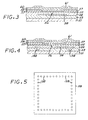
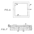
- the thin film heater substructure 11 includes a plurality of resistors 56, and a plurality of thermally conductive regions 58 respectively associated with and underlying the heater resistors 56 for dissipating heat from the associated heater resistors 56.
- the heater resistors 56 comprise thin film resistors
- the thermally conductive regions comprise metal regions or slabs.
- the thermally conductive regions associated with heater resistors close to the edges of the thin film heater substructure are not shown so as to indicate that such thermally conductive regions do not extend laterally beyond their associated heater resistors.
- the thermal dissipation characteristics, pattern, or profile of the thin film heater substructure 11 is tuned by varying or selecting the areas of the thermally conductive regions as a function of location in the thin film sub-structure.
- the metallization layer 57 comprises metallization traces defined by appropriate masking and etching. The masking and etch of the metallization layer 57 also defines the resistor areas.
- the resistive layer 55 and the metallization layer 57 are generally in registration with each other, except that portions of traces of the metallization layer 57 are removed in those areas where heater resistors are formed.
- the conductive path at an opening in a trace in the metallization layer 57 includes a portion of the resistive layer 55 located at the opening or gap in the conductive trace.
- a resistor area is defined by providing first and second metallic traces that terminate at different locations on the perimeter of the resistor area.
- the metal subareas 58 underlie and are proximate to associated heater resistors 56, and comprise heat dissipating thermally conductive regions.
- the areas of the metal subareas which are generally planar, are individually configured to achieve a desired heat dissipation capacity for the laminar heater resistor structure formed by the heater resistor and the associated metal subarea. This allows for tailoring of the thermal characteristic of the thin film heater substructure 11.
Landscapes
- Physics & Mathematics (AREA)
- General Physics & Mathematics (AREA)
- Optics & Photonics (AREA)
- Nonlinear Science (AREA)
- Resistance Heating (AREA)
- Mechanical Light Control Or Optical Switches (AREA)
- Surface Heating Bodies (AREA)
- Control Of Resistance Heating (AREA)
- Electrochromic Elements, Electrophoresis, Or Variable Reflection Or Absorption Elements (AREA)
Abstract
Description
Claims (13)
- A heater resistor array comprising:a thin film substructure (11);a plurality of heater resistors (56) formed in said thin film substructure; anda plurality of thermally conductive regions (58) respectively associated with said heater resistors and dielectrically separated from said heater resistors, each of said thermally conductive regions being located proximately to an associated one of said heater resistors for dissipating heat from said associated heater resistor, wherein said thermally conductive regions have respective areas that are selected so as to tailor respective heat dissipation capacities of associated ones of said heater resistors.
- The heater resistor array of Claim 1 wherein said heater resistors comprise planar heater resistors, and wherein said thermally conductive regions comprise planar thermally conductive regions.
- The heater resistor array of Claim 2 wherein said planar thermally conductive regions comprise planar metal regions.
- The heater resistor array of Claim 3 wherein said planar heater resistors are separated from said planar metal regions by silicon dioxide (53).
- The heater resistor array of Claim 4 wherein said thin film substructure includes a silicon substrate (51).
- The heater resistor array of Claim 1 wherein said thin film substructure includes a silicon substrate (51), and wherein said thermally conductive regions comprise metal regions.
- The heater resistor array of Claim 6 wherein said metal regions are contacted to said silicon substrate.
- The heater resistor array of Claim 7 further including metal vias (158) for contacting said metal regions to said silicon substrate.
- The heater resistor array of Claim 7 wherein said metal regions comprise metal contact slabs.
- The heater resistor array of Claim 1 wherein said areas of said thermally conducting regions vary depending on locations of respective thermally conductive regions in said thin film substructure.
- The heater resistor array of Claim 10 herein thermally conductive regions in a middle portion of said thin film substructure have respective areas that are greater than areas of thermally conductive regions near edges of said thin film substructure.
- The heater resistor array of Claim 10 herein thermally conductive regions in a middle portion of said thin film substructure have respective areas that are smaller than areas of thermally conductive regions near edges of said thin film substructure.
- The heater resistor array of Claim 1 further including a waveguide substrate (13) adjacent to said thin film substructure having a plurality of fluidic optical switching elements that are actuated by thermal energy from said heater resistors.
Applications Claiming Priority (2)
| Application Number | Priority Date | Filing Date | Title |
|---|---|---|---|
| US493950 | 2000-01-28 | ||
| US09/493,950 US6314216B1 (en) | 2000-01-28 | 2000-01-28 | Resistor array with position dependent heat dissipation |
Publications (3)
| Publication Number | Publication Date |
|---|---|
| EP1130444A2 true EP1130444A2 (en) | 2001-09-05 |
| EP1130444A3 EP1130444A3 (en) | 2002-07-10 |
| EP1130444B1 EP1130444B1 (en) | 2004-03-31 |
Family
ID=23962384
Family Applications (1)
| Application Number | Title | Priority Date | Filing Date |
|---|---|---|---|
| EP01300343A Expired - Lifetime EP1130444B1 (en) | 2000-01-28 | 2001-01-16 | Resistor array with position dependent heat dissipation |
Country Status (8)
| Country | Link |
|---|---|
| US (2) | US6314216B1 (en) |
| EP (1) | EP1130444B1 (en) |
| JP (1) | JP3936536B2 (en) |
| KR (1) | KR100751178B1 (en) |
| CN (1) | CN1162730C (en) |
| BR (1) | BR0100261A (en) |
| DE (1) | DE60102502T2 (en) |
| TW (1) | TW451070B (en) |
Families Citing this family (13)
| Publication number | Priority date | Publication date | Assignee | Title |
|---|---|---|---|---|
| US7344894B2 (en) * | 2001-10-16 | 2008-03-18 | Agilent Technologies, Inc. | Thermal regulation of fluidic samples within a diagnostic cartridge |
| US7398209B2 (en) * | 2002-06-03 | 2008-07-08 | Voicebox Technologies, Inc. | Systems and methods for responding to natural language speech utterance |
| US7025893B2 (en) * | 2003-08-12 | 2006-04-11 | Thermo Stone Usa, Llc | Structure and method to compensate for thermal edge loss in thin film heaters |
| US6946718B2 (en) * | 2004-01-05 | 2005-09-20 | Hewlett-Packard Development Company, L.P. | Integrated fuse for multilayered structure |
| WO2005069858A2 (en) * | 2004-01-16 | 2005-08-04 | Northern Illinois University | Nano-composite piezoelectric material |
| US7286359B2 (en) * | 2004-05-11 | 2007-10-23 | The U.S. Government As Represented By The National Security Agency | Use of thermally conductive vias to extract heat from microelectronic chips and method of manufacturing |
| US7187487B2 (en) * | 2004-07-30 | 2007-03-06 | Hewlett-Packard Development Company, L.P. | Light modulator with a light-absorbing layer |
| US20080298737A1 (en) * | 2007-06-04 | 2008-12-04 | Lumera Corporation | Integrated Resistor Fabrication Method and Optical Devices Therefrom |
| TWI369693B (en) * | 2008-04-10 | 2012-08-01 | Ind Tech Res Inst | Thin film resistor structure and fabrication method thereof |
| JP5842781B2 (en) * | 2012-05-23 | 2016-01-13 | 株式会社デンソー | Radiation heater device |
| JP6447753B2 (en) * | 2016-01-25 | 2019-01-09 | 株式会社デンソー | Heater device |
| US9768093B1 (en) | 2016-03-04 | 2017-09-19 | Altera Corporation | Resistive structure with enhanced thermal dissipation |
| CN110716302A (en) * | 2019-10-25 | 2020-01-21 | 德淮半导体有限公司 | Optical element, aberration correction device, lithography machine system and aberration correction method |
Family Cites Families (9)
| Publication number | Priority date | Publication date | Assignee | Title |
|---|---|---|---|---|
| GB8521931D0 (en) * | 1985-09-04 | 1985-10-09 | British Aerospace | Thermal image producing device |
| US4988157A (en) * | 1990-03-08 | 1991-01-29 | Bell Communications Research, Inc. | Optical switch using bubbles |
| JP2651496B2 (en) * | 1990-04-06 | 1997-09-10 | セイコー電子工業株式会社 | Thermal head |
| US5414245A (en) * | 1992-08-03 | 1995-05-09 | Hewlett-Packard Corporation | Thermal-ink heater array using rectifying material |
| US5357271A (en) * | 1993-01-19 | 1994-10-18 | Intermec Corporation | Thermal printhead with enhanced laterla heat conduction |
| JPH0722547A (en) * | 1993-06-29 | 1995-01-24 | Kawasaki Steel Corp | Semiconductor device |
| JP3290268B2 (en) | 1993-10-21 | 2002-06-10 | 日鉄鉱業株式会社 | Filter element |
| US5699462A (en) * | 1996-06-14 | 1997-12-16 | Hewlett-Packard Company | Total internal reflection optical switches employing thermal activation |
| US5960131A (en) * | 1998-02-04 | 1999-09-28 | Hewlett-Packard Company | Switching element having an expanding waveguide core |
-
2000
- 2000-01-28 US US09/493,950 patent/US6314216B1/en not_active Expired - Fee Related
- 2000-10-21 TW TW089121815A patent/TW451070B/en not_active IP Right Cessation
- 2000-12-28 CN CNB00129475XA patent/CN1162730C/en not_active Expired - Fee Related
-
2001
- 2001-01-09 BR BR0100261-9A patent/BR0100261A/en not_active Application Discontinuation
- 2001-01-16 DE DE60102502T patent/DE60102502T2/en not_active Expired - Lifetime
- 2001-01-16 EP EP01300343A patent/EP1130444B1/en not_active Expired - Lifetime
- 2001-01-26 KR KR1020010003678A patent/KR100751178B1/en not_active Expired - Fee Related
- 2001-01-29 JP JP2001019897A patent/JP3936536B2/en not_active Expired - Fee Related
- 2001-09-14 US US09/952,923 patent/US6549690B2/en not_active Expired - Fee Related
Also Published As
| Publication number | Publication date |
|---|---|
| TW451070B (en) | 2001-08-21 |
| US20020015550A1 (en) | 2002-02-07 |
| DE60102502D1 (en) | 2004-05-06 |
| US6314216B1 (en) | 2001-11-06 |
| US6549690B2 (en) | 2003-04-15 |
| JP3936536B2 (en) | 2007-06-27 |
| KR100751178B1 (en) | 2007-08-22 |
| DE60102502T2 (en) | 2005-03-03 |
| KR20010078058A (en) | 2001-08-20 |
| EP1130444B1 (en) | 2004-03-31 |
| BR0100261A (en) | 2001-08-28 |
| JP2001255475A (en) | 2001-09-21 |
| CN1319772A (en) | 2001-10-31 |
| CN1162730C (en) | 2004-08-18 |
| EP1130444A3 (en) | 2002-07-10 |
Similar Documents
| Publication | Publication Date | Title |
|---|---|---|
| US6314216B1 (en) | Resistor array with position dependent heat dissipation | |
| TW503575B (en) | Semiconductor device having passive elements and method of making same | |
| US6977196B1 (en) | Micro-electromechanical switch fabricated by simultaneous formation of a resistor and bottom electrode | |
| KR100742023B1 (en) | Semiconductor device and manufacturing method thereof | |
| KR100697405B1 (en) | Electronic devices | |
| KR100395182B1 (en) | Electronic components with thin film structure with passive elements | |
| EP0769813A3 (en) | Integrated circuit with planarized dielectric layer between successive polysilicon layers | |
| KR20040049872A (en) | Semiconductor device and method for the same | |
| KR0179838B1 (en) | Structure of insulating film semiconductor device and method of planarizing insulating film | |
| KR100331226B1 (en) | microwave electric elements of using porous oxidized silicon pole | |
| KR20030083174A (en) | Method of providing air gap in process of semiconductor | |
| US20050077540A1 (en) | Integrated circuit arrangement | |
| JP2975711B2 (en) | Multilayer wiring board with built-in termination resistor | |
| KR0161424B1 (en) | Wiring layer of integrated circuit device | |
| KR0161458B1 (en) | Planerizing method of semiconductor device | |
| KR100524907B1 (en) | Metalliation method for semiconductor device | |
| KR100275940B1 (en) | Method of fabricating an interlayer in semiconductor devices | |
| KR20010059181A (en) | Method for forming contact plug of semiconductor device | |
| KR0163867B1 (en) | Pcb having a t-conductive wire and the manufacture thereof | |
| KR100529612B1 (en) | Manufacturing method of semiconductor device | |
| KR100313942B1 (en) | Method for Forming Contact Hole of Semiconductor Device | |
| KR100379900B1 (en) | microwave electric elements fabricated using porous oxidized silicon layer and fabricating method of the same | |
| KR19980065695A (en) | Inductor Manufacturing | |
| KR100485181B1 (en) | a contact structure for interconnecting multi-level wires and a method for forming the same | |
| KR100228278B1 (en) | Manufacturing Method of Semiconductor Device |
Legal Events
| Date | Code | Title | Description |
|---|---|---|---|
| PUAI | Public reference made under article 153(3) epc to a published international application that has entered the european phase |
Free format text: ORIGINAL CODE: 0009012 |
|
| AK | Designated contracting states |
Kind code of ref document: A2 Designated state(s): AT BE CH CY DE DK ES FI FR GB GR IE IT LI LU MC NL PT SE TR |
|
| AX | Request for extension of the european patent |
Free format text: AL;LT;LV;MK;RO;SI |
|
| PUAL | Search report despatched |
Free format text: ORIGINAL CODE: 0009013 |
|
| AK | Designated contracting states |
Kind code of ref document: A3 Designated state(s): AT BE CH CY DE DK ES FI FR GB GR IE IT LI LU MC NL PT SE TR |
|
| AX | Request for extension of the european patent |
Free format text: AL;LT;LV;MK;RO;SI |
|
| RIC1 | Information provided on ipc code assigned before grant |
Free format text: 7G 02B 26/02 A, 7B 41J 2/14 B |
|
| 17P | Request for examination filed |
Effective date: 20021220 |
|
| 17Q | First examination report despatched |
Effective date: 20030128 |
|
| AKX | Designation fees paid |
Designated state(s): DE FR GB |
|
| GRAP | Despatch of communication of intention to grant a patent |
Free format text: ORIGINAL CODE: EPIDOSNIGR1 |
|
| GRAS | Grant fee paid |
Free format text: ORIGINAL CODE: EPIDOSNIGR3 |
|
| GRAA | (expected) grant |
Free format text: ORIGINAL CODE: 0009210 |
|
| AK | Designated contracting states |
Kind code of ref document: B1 Designated state(s): DE FR GB |
|
| REG | Reference to a national code |
Ref country code: GB Ref legal event code: FG4D |
|
| REG | Reference to a national code |
Ref country code: IE Ref legal event code: FG4D |
|
| REF | Corresponds to: |
Ref document number: 60102502 Country of ref document: DE Date of ref document: 20040506 Kind code of ref document: P |
|
| ET | Fr: translation filed | ||
| PLBE | No opposition filed within time limit |
Free format text: ORIGINAL CODE: 0009261 |
|
| STAA | Information on the status of an ep patent application or granted ep patent |
Free format text: STATUS: NO OPPOSITION FILED WITHIN TIME LIMIT |
|
| 26N | No opposition filed |
Effective date: 20050104 |
|
| REG | Reference to a national code |
Ref country code: GB Ref legal event code: 732E Free format text: REGISTERED BETWEEN 20120329 AND 20120404 |
|
| PGFP | Annual fee paid to national office [announced via postgrant information from national office to epo] |
Ref country code: GB Payment date: 20131223 Year of fee payment: 14 |
|
| PGFP | Annual fee paid to national office [announced via postgrant information from national office to epo] |
Ref country code: DE Payment date: 20131219 Year of fee payment: 14 |
|
| PGFP | Annual fee paid to national office [announced via postgrant information from national office to epo] |
Ref country code: FR Payment date: 20140120 Year of fee payment: 14 |
|
| REG | Reference to a national code |
Ref country code: DE Ref legal event code: R119 Ref document number: 60102502 Country of ref document: DE |
|
| GBPC | Gb: european patent ceased through non-payment of renewal fee |
Effective date: 20150116 |
|
| PG25 | Lapsed in a contracting state [announced via postgrant information from national office to epo] |
Ref country code: GB Free format text: LAPSE BECAUSE OF NON-PAYMENT OF DUE FEES Effective date: 20150116 Ref country code: DE Free format text: LAPSE BECAUSE OF NON-PAYMENT OF DUE FEES Effective date: 20150801 |
|
| REG | Reference to a national code |
Ref country code: FR Ref legal event code: ST Effective date: 20150930 |
|
| PG25 | Lapsed in a contracting state [announced via postgrant information from national office to epo] |
Ref country code: FR Free format text: LAPSE BECAUSE OF NON-PAYMENT OF DUE FEES Effective date: 20150202 |