EP1126558A2 - ZEE elektrische Verbindung - Google Patents
ZEE elektrische Verbindung Download PDFInfo
- Publication number
- EP1126558A2 EP1126558A2 EP00127297A EP00127297A EP1126558A2 EP 1126558 A2 EP1126558 A2 EP 1126558A2 EP 00127297 A EP00127297 A EP 00127297A EP 00127297 A EP00127297 A EP 00127297A EP 1126558 A2 EP1126558 A2 EP 1126558A2
- Authority
- EP
- European Patent Office
- Prior art keywords
- interconnect
- elements
- base
- set forth
- conductors
- Prior art date
- Legal status (The legal status is an assumption and is not a legal conclusion. Google has not performed a legal analysis and makes no representation as to the accuracy of the status listed.)
- Withdrawn
Links
Images
Classifications
-
- H—ELECTRICITY
- H01—ELECTRIC ELEMENTS
- H01R—ELECTRICALLY-CONDUCTIVE CONNECTIONS; STRUCTURAL ASSOCIATIONS OF A PLURALITY OF MUTUALLY-INSULATED ELECTRICAL CONNECTING ELEMENTS; COUPLING DEVICES; CURRENT COLLECTORS
- H01R13/00—Details of coupling devices of the kinds covered by groups H01R12/70 or H01R24/00 - H01R33/00
- H01R13/46—Bases; Cases
- H01R13/533—Bases, cases made for use in extreme conditions, e.g. high temperature, radiation, vibration, corrosive environment, pressure
-
- H—ELECTRICITY
- H01—ELECTRIC ELEMENTS
- H01R—ELECTRICALLY-CONDUCTIVE CONNECTIONS; STRUCTURAL ASSOCIATIONS OF A PLURALITY OF MUTUALLY-INSULATED ELECTRICAL CONNECTING ELEMENTS; COUPLING DEVICES; CURRENT COLLECTORS
- H01R13/00—Details of coupling devices of the kinds covered by groups H01R12/70 or H01R24/00 - H01R33/00
- H01R13/02—Contact members
- H01R13/04—Pins or blades for co-operation with sockets
- H01R13/05—Resilient pins or blades
Definitions
- the present invention relates to electrical interconnects, and more particularly to an interconnect for electrically connecting two conductors separated by some length which repeatedly expands and contracts.
- An important source of electrical power for an orbiting satellite is its solar array.
- an electrical connection is typically made between the solar cell circuits, which convert solar energy into electrical energy, and an electrical wiring harness, which conducts the electrical energy into the spacecraft.
- Such connections and the substrates to which they are mounted are subject to cyclical, extreme variations in temperature. These variations occur as the satellite orbits the earth. They result from the satellite being in complete sunlight at some times and being in the shadow of the earth at other times.
- These temperature variations along with the coefficient of thermal expansion of the substrate, which carries the solar cell circuits and harness, cause a change in distance between those components.
- the unstressed length of the electrical connection which connects the circuits and the harness, changes, but by a different amount. As the substrate is generally stiffer than the electrical connection, the electrical connection is stressed.
- a prior solution to the problem was the use of a conductor in the form of a ribbon electrical interconnect which had a half-loop formed intermediate to its ends to relieve stress.
- the stress relief improved performance compared to a flat conductor but was found inadequate for spacecraft that had many tens of thousands of repeated movements between the connected points.
- interconnect for electrically connecting the harness to the solar cell circuits that can accommodate the repeated changes in temperature.
- interconnect must be low in height to accommodate the packing requirements for some solar arrays.
- the interconnect includes a base element, an intermediate element and a top element.
- Each element is comprised of an electrically conducting material.
- the elements are arranged in a generally Z-shape with the free end of the base element connected to one conductor and the free end of the top element connected to the other conductor.
- the intermediate element has its ends disposed adjacent to corresponding ends of the base and the top elements. Brazes electrically and mechanically secure the intermediate element to the respective base and top elements which proximate the corresponding free ends of the elements.
- This configuration enables the three elements to accommodate changes in the separation distance between the conductors and to absorb the associated compression and tension forces on the elements.
- the increased length of the conductive elements compared to prior art elements, enables them to be less stressed by dramatic changes in the temperature of the environment.
- the present invention relates to an interconnect for electrically connecting two conductors separated by some length which remains fixed while the unstressed length of the interconnect changes, generally due to its coefficient of thermal expansion as it is heated or cooled. It also relates to an interconnect for electrically connecting two conductors separated by some length which expands and contracts while the unstressed length of the interconnect also expands and contracts, but at a different rate. More succinctly, the invention, having some length, reliably connects two conductors separated by the same length when the connection is made; but in which the one unstressed length cyclically changes relative to the other in operation.
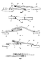
- FIG. 1 diagrammatically illustrates the interconnect in accordance with the present invention.
- FIG. 2 is a top plan view of the interconnect illustrated in FIG. 1.
- FIG. 3 is a diagrammatic representation of the interconnect shown in FIG. 1 when it is subjected to compression.
- FIG. 4 is a diagrammatic representation of the interconnect shown in FIG. 1 when it is subjected tension.
- FIG. 5 is an alternative embodiment of the interconnect.
- FIG. 1 and FIG. 2 illustrate the invention.
- the invention is generally designated by the numeral 10.
- the interconnect 10 includes a base element 12, an intermediate element 14 and a top element 16.
- Each element 12, 14 and 16 has an elongated shape with a rectangular cross section such that it appears to resemble a ribbon, and is formed from an electrically conducting material, such as copper, KovarTM or other conductor.
- the elements are arranged in a compact Z-shape with a relatively small height as measured from the bottom surface of he base element 12 to the uppermost area of the top surface 16.
- the intermediate element is arranged with its ends 26 and 28 disposed against the end 30 of the base element and the end 32 of the top element 16.
- Two brazes 34 secure the intermediate element 14 to the base element 12 and two brazes 36 to secure it to the top element 16 at locations proximate the ends of the elements.
- the base element 12 and the top element 16 are secured to the contacts 20 on the respective conductors 22 and 24 by solder, although small rivets, brazing, or the like can also be used. Thus electrical continuity between the conductors is achieved.
- brazed joints are replaced with solder joints . or with any similar means of making the physical and electrical connection between the base, intermediate and top elements.
- the interconnect 10 provides a continuous electrical path from the contact 20 on conductor 22 through the elements 12, 14 and 16 to the contact 20 on conductor 24.
- the conductors 22 and 24, respectively, serve to mount solar cell circuits on a solar cell panel or blanket and an electrical wiring harness.
- the solar cell circuits are generally used on orbiting satellites to receive solar energy and convert it into electrical energy to power the electrical equipment in the satellite.
- the solar cell blanket or panels extend from the satellite and are therefore subject to extreme temperature changes. Because of temperature changes, the surfaces containing the solar cell circuits and the wiring harness constantly change position (both vertically and horizontally as shown in FIG. 1) and exhibit many contractions or expansions in distance therebetween. This induces both compression and expansion in the interconnect and could induce stresses to the contacts for solar cell circuits and the wiring harness.
- the interconnect 10 spreads the strain due to length change over an area of the body of the base, the intermediate and the top elements. This enables the interconnect to undergo repeated compression and expansion cycles without cracking.
- the conductive material of the interconnect has a characteristic stiffness that is less than that of the platform on which the conductors are fixed, it is the conductive material that bends and not the platform
- FIGs. 3 and 4 the functional operation of the interconnect is . shown when subjected to compression and expansion.
- FIG. 3 effects of compression are illustrated.
- the distance between the contacts 20 of the separated conductors 22 and 24 is smaller or the length of the interconnect has increased from that illustrated in FIG. 1 and the interconnect has a shape in which the base element 12 bends upwardly, the intermediate element 14 curves so that its end 28 is adjacent the base element 12 and the top element 16 curves as shown.
- FIG. 4 the interconnect is shown under expansion whereby the distance between the contacts 20 is greater and/or the length of the interconnect has decreased from that illustrated in FIG. 1.
- the base element 12 is curved "down" slightly, the intermediate element 14 separates from the base element 12 with a curved shape and the top element 16 has a generally curved shape.
- the interconnect absorbed the change by bending in a manner that reduces fatigue to negligible levels.
- the prior art interconnect having a half-loop formed in the conducting material so as to relieve strain concentrates the bending at the top of its half loop. Therefore, the prior art interconnect undergoes stress that is much higher at the top of the loop and under repeated cycling has been found to fail.
- Displacement tests on interconnects 10 formed in accordance with the present invention produced the following results. In the tests, the greater the displacement, the more likely it is that an interconnect will fail at a lower number of displacement cycles. In five of the six tests conducted, the interconnect of the present invention did not fail before the test was stopped. More particularly, six interconnects that were annealed, 0.2 inches wide, 0.6 inches high and 4.0 inches in length with brazes to secure the elements and six interconnects having the same characteristics except that the height was 0.5 inches high were subject to displacement tests. In this, the interconnects were displaced ⁇ 0.015 inches over 1,000,000 cycles without failing. In contrast, two tests on prior art interconnects with the half-loop stress relief portion were tested to a lesser displacement of ⁇ 0.006 inches. One failed at 23,689 cycles and the other failed at 71,431 cycles.
- the interconnect 10 has base 12, intermediate 14, and top 16 elements that are formed from an integral piece of conductive material such as copper or KovarTM.
- the embodiment illustrated conducts electrical current between separated conductors and operates in exactly the same manner as that previously described.
- an improved interconnect for mechanically and electrically connecting contacts on separated moveable surfaces that is of low height and withstands changes in temperature and displacement is provided.
Landscapes
- Photovoltaic Devices (AREA)
- Wire Bonding (AREA)
Applications Claiming Priority (2)
| Application Number | Priority Date | Filing Date | Title |
|---|---|---|---|
| US501412 | 2000-02-09 | ||
| US09/501,412 US6293803B1 (en) | 2000-02-09 | 2000-02-09 | Zee electrical interconnect |
Publications (1)
| Publication Number | Publication Date |
|---|---|
| EP1126558A2 true EP1126558A2 (de) | 2001-08-22 |
Family
ID=23993459
Family Applications (1)
| Application Number | Title | Priority Date | Filing Date |
|---|---|---|---|
| EP00127297A Withdrawn EP1126558A2 (de) | 2000-02-09 | 2000-12-19 | ZEE elektrische Verbindung |
Country Status (3)
| Country | Link |
|---|---|
| US (1) | US6293803B1 (de) |
| EP (1) | EP1126558A2 (de) |
| JP (1) | JP2001291891A (de) |
Cited By (10)
| Publication number | Priority date | Publication date | Assignee | Title |
|---|---|---|---|---|
| USD573539S1 (en) | 2007-08-09 | 2008-07-22 | Solar Watt Ag | Sinusoidal connection band without stabilizing plate |
| USD573538S1 (en) | 2007-08-09 | 2008-07-22 | Solar Watt Ag | Middle Z-connector with outer C-connector |
| USD574327S1 (en) | 2007-08-09 | 2008-08-05 | Solarwatt Ag | Sinusoidal connection band and stabilizing plate |
| USD574777S1 (en) | 2007-08-09 | 2008-08-12 | Solarwatt Ag | C-connector |
| USD574776S1 (en) | 2007-08-09 | 2008-08-12 | Solarwatt Ag | Omega-connector |
| USD575233S1 (en) | 2007-08-09 | 2008-08-19 | Solar Watt Ag | Middle Z-connector with outer V-connector |
| USD585023S1 (en) | 2007-11-26 | 2009-01-20 | Solarwatt Ag | Simple c-connector |
| USD589883S1 (en) | 2007-11-26 | 2009-04-07 | Solarwatt Ag | Z-connector |
| WO2009049572A1 (de) | 2007-10-19 | 2009-04-23 | Solarwatt Ag | Leitungsverbinder für solarzellen von plattenförmigen solarmodulen |
| WO2010133224A2 (de) | 2009-05-18 | 2010-11-25 | Solarion Ag | Anordnung und verschaltung, sowie verfahren zur verschaltung von flächenartigen solarzellen |
Families Citing this family (20)
| Publication number | Priority date | Publication date | Assignee | Title |
|---|---|---|---|---|
| JP3895908B2 (ja) * | 2000-06-30 | 2007-03-22 | 矢崎総業株式会社 | スライドドア用ハーネスの配索構造 |
| US6722892B1 (en) * | 2002-12-19 | 2004-04-20 | General Electric Company | Multi-plane adjustable connector |
| US20040222422A1 (en) * | 2003-05-08 | 2004-11-11 | Wein-Town Sun | CMOS inverter layout |
| US7910822B1 (en) | 2005-10-17 | 2011-03-22 | Solaria Corporation | Fabrication process for photovoltaic cell |
| US8227688B1 (en) | 2005-10-17 | 2012-07-24 | Solaria Corporation | Method and resulting structure for assembling photovoltaic regions onto lead frame members for integration on concentrating elements for solar cells |
| DE102006025867A1 (de) * | 2006-06-02 | 2007-12-06 | Robert Bosch Gmbh | Bondverbindung sowie Verfahren zum Bonden zweier Kontaktflächen |
| JP5057805B2 (ja) * | 2007-03-12 | 2012-10-24 | シャープ株式会社 | 太陽電池アレイ、太陽電池モジュールおよび太陽電池アレイの製造方法 |
| US7910392B2 (en) | 2007-04-02 | 2011-03-22 | Solaria Corporation | Method and system for assembling a solar cell package |
| US20090056806A1 (en) * | 2007-09-05 | 2009-03-05 | Solaria Corporation | Solar cell structure including a plurality of concentrator elements with a notch design and predetermined radii and method |
| US8119902B2 (en) | 2007-05-21 | 2012-02-21 | Solaria Corporation | Concentrating module and method of manufacture for photovoltaic strips |
| US7419377B1 (en) * | 2007-08-20 | 2008-09-02 | Solaria Corporation | Electrical coupling device and method for solar cells |
| US7625516B2 (en) * | 2007-08-31 | 2009-12-01 | C.I. Kasei Company, Limited | Method for manufacturing sheet molded body and insert molded body |
| US7910035B2 (en) | 2007-12-12 | 2011-03-22 | Solaria Corporation | Method and system for manufacturing integrated molded concentrator photovoltaic device |
| ES2512016T5 (es) * | 2009-06-08 | 2018-12-28 | Auto-Kabel Management Gmbh | Conector de elementos de batería |
| US20120211050A1 (en) * | 2009-12-25 | 2012-08-23 | Mitsubishi Electric Corporation | Solar battery module |
| US8637771B1 (en) * | 2010-02-26 | 2014-01-28 | Greald W Yankie | Electromotive coil with improved conductor packing ratio |
| CN102263345A (zh) * | 2010-05-24 | 2011-11-30 | 鸿富锦精密工业(深圳)有限公司 | 连接件 |
| USD699176S1 (en) | 2011-06-02 | 2014-02-11 | Solaria Corporation | Fastener for solar modules |
| JP5832918B2 (ja) * | 2012-02-07 | 2015-12-16 | シャープ株式会社 | 太陽電池セル、太陽電池アレイおよび太陽電池アレイの製造方法 |
| JP6741215B2 (ja) * | 2017-01-20 | 2020-08-19 | 株式会社オートネットワーク技術研究所 | 接続モジュール |
Family Cites Families (4)
| Publication number | Priority date | Publication date | Assignee | Title |
|---|---|---|---|---|
| US2865979A (en) * | 1955-10-14 | 1958-12-23 | Teletype Corp | Extensible cable structure |
| US3488430A (en) * | 1967-12-13 | 1970-01-06 | Honeywell Inc | Retractable cable forming clip |
| US3676572A (en) * | 1971-06-01 | 1972-07-11 | Barber Colman Co | Extensible cable structure |
| DE4033880A1 (de) * | 1990-10-25 | 1992-04-30 | Triumph Adler Ag | Kabelanordnung |
-
2000
- 2000-02-09 US US09/501,412 patent/US6293803B1/en not_active Expired - Lifetime
- 2000-12-19 EP EP00127297A patent/EP1126558A2/de not_active Withdrawn
-
2001
- 2001-02-09 JP JP2001033605A patent/JP2001291891A/ja active Pending
Cited By (11)
| Publication number | Priority date | Publication date | Assignee | Title |
|---|---|---|---|---|
| USD573539S1 (en) | 2007-08-09 | 2008-07-22 | Solar Watt Ag | Sinusoidal connection band without stabilizing plate |
| USD573538S1 (en) | 2007-08-09 | 2008-07-22 | Solar Watt Ag | Middle Z-connector with outer C-connector |
| USD574327S1 (en) | 2007-08-09 | 2008-08-05 | Solarwatt Ag | Sinusoidal connection band and stabilizing plate |
| USD574777S1 (en) | 2007-08-09 | 2008-08-12 | Solarwatt Ag | C-connector |
| USD574776S1 (en) | 2007-08-09 | 2008-08-12 | Solarwatt Ag | Omega-connector |
| USD575233S1 (en) | 2007-08-09 | 2008-08-19 | Solar Watt Ag | Middle Z-connector with outer V-connector |
| WO2009049572A1 (de) | 2007-10-19 | 2009-04-23 | Solarwatt Ag | Leitungsverbinder für solarzellen von plattenförmigen solarmodulen |
| USD585023S1 (en) | 2007-11-26 | 2009-01-20 | Solarwatt Ag | Simple c-connector |
| USD589883S1 (en) | 2007-11-26 | 2009-04-07 | Solarwatt Ag | Z-connector |
| WO2010133224A2 (de) | 2009-05-18 | 2010-11-25 | Solarion Ag | Anordnung und verschaltung, sowie verfahren zur verschaltung von flächenartigen solarzellen |
| DE102010016975A1 (de) | 2009-05-18 | 2011-01-05 | Solarion Ag | Anordnung und Verschaltung, sowie Verfahren zur Verschaltung von flächenartigen Solarzellen |
Also Published As
| Publication number | Publication date |
|---|---|
| JP2001291891A (ja) | 2001-10-19 |
| US6293803B1 (en) | 2001-09-25 |
Similar Documents
| Publication | Publication Date | Title |
|---|---|---|
| US6293803B1 (en) | Zee electrical interconnect | |
| EP0848449B1 (de) | Geschweisstes Drahtanschlusstück und Verfahren zu seiner Herstellung | |
| US4751199A (en) | Process of forming a compliant lead frame for array-type semiconductor packages | |
| US3870568A (en) | Heat generator | |
| US5650914A (en) | Compliant thermal connectors, methods of making the same and assemblies incorporating the same | |
| US5588848A (en) | Low inductance surface-mount connectors for interconnecting circuit devices and method for using same | |
| KR100537870B1 (ko) | 컨택트 시트, 그 제조 방법, 그리고 그것을 구비한 소켓 | |
| US4688151A (en) | Multilayered interposer board for powering high current chip modules | |
| KR0145275B1 (ko) | 회로장치 | |
| US6884653B2 (en) | Folded interposer | |
| EP1088470B1 (de) | Flexschaltung verwendender ic-stapel mit km-kontakten | |
| US5214563A (en) | Thermally reactive lead assembly and method for making same | |
| WO1996016532A9 (en) | Compliant thermal connectors, methods and assemblies | |
| JP2002522926A (ja) | 可撓性を有する折畳み可能な宇宙飛行体用の太陽発電機 | |
| WO2014062559A2 (en) | Structures and methods for multi-leg package thermoelectric devices | |
| US7293995B2 (en) | Electrical contact and connector system | |
| US6489564B2 (en) | Stress relieving tape bonding interconnect | |
| Rust et al. | Zee electrical interconnect | |
| KR19990037330A (ko) | 기억금속을 이용한 풀 웨이퍼 테스트 장치 | |
| US7066740B2 (en) | Area array package with low inductance connecting device | |
| EP0146463B1 (de) | Elastisches Verbindungselement für die Oberflächenmontage von Halbleiterelementen | |
| JPH1117234A (ja) | 熱電気変換装置 | |
| WO2001043513A1 (en) | Mounting electrical devices to circuit boards | |
| TW202044678A (zh) | 具有旁路電容器的電源插入器 | |
| KR930703703A (ko) | 집적회로 다이-리드프레임 연결 어셈블리 시스템 |
Legal Events
| Date | Code | Title | Description |
|---|---|---|---|
| PUAI | Public reference made under article 153(3) epc to a published international application that has entered the european phase |
Free format text: ORIGINAL CODE: 0009012 |
|
| AK | Designated contracting states |
Kind code of ref document: A2 Designated state(s): AT BE CH CY DE DK ES FI FR GB GR IE IT LI LU MC NL PT SE TR |
|
| AX | Request for extension of the european patent |
Free format text: AL;LT;LV;MK;RO;SI |
|
| RAP1 | Party data changed (applicant data changed or rights of an application transferred) |
Owner name: THE UNITED STATES OF AMERICA, REPRESENTED BY THE Owner name: TRW INC. |
|
| RIN1 | Information on inventor provided before grant (corrected) |
Inventor name: PATTERSON, ROBERT E. Inventor name: RUST, THOMAS M. Inventor name: HERRIAGE, MICHAEL J. Inventor name: GADDY, EDWARD M. Inventor name: PARTIN, RICHARD D. |
|
| STAA | Information on the status of an ep patent application or granted ep patent |
Free format text: STATUS: THE APPLICATION HAS BEEN WITHDRAWN |
|
| 18W | Application withdrawn |
Withdrawal date: 20020930 |