EP1126479A1 - Résistance haute tension, notamment de limitation de courant dans un émetteur à tube hyperfréquence à onde progressive - Google Patents
Résistance haute tension, notamment de limitation de courant dans un émetteur à tube hyperfréquence à onde progressive Download PDFInfo
- Publication number
- EP1126479A1 EP1126479A1 EP01400289A EP01400289A EP1126479A1 EP 1126479 A1 EP1126479 A1 EP 1126479A1 EP 01400289 A EP01400289 A EP 01400289A EP 01400289 A EP01400289 A EP 01400289A EP 1126479 A1 EP1126479 A1 EP 1126479A1
- Authority
- EP
- European Patent Office
- Prior art keywords
- resistor according
- flat conductor
- resistance
- resistor
- support
- Prior art date
- Legal status (The legal status is an assumption and is not a legal conclusion. Google has not performed a legal analysis and makes no representation as to the accuracy of the status listed.)
- Granted
Links
Images



Classifications
-
- H—ELECTRICITY
- H01—ELECTRIC ELEMENTS
- H01C—RESISTORS
- H01C7/00—Non-adjustable resistors formed as one or more layers or coatings; Non-adjustable resistors made from powdered conducting material or powdered semi-conducting material with or without insulating material
- H01C7/10—Non-adjustable resistors formed as one or more layers or coatings; Non-adjustable resistors made from powdered conducting material or powdered semi-conducting material with or without insulating material voltage responsive, i.e. varistors
- H01C7/12—Overvoltage protection resistors; Arresters
-
- H—ELECTRICITY
- H01—ELECTRIC ELEMENTS
- H01C—RESISTORS
- H01C7/00—Non-adjustable resistors formed as one or more layers or coatings; Non-adjustable resistors made from powdered conducting material or powdered semi-conducting material with or without insulating material
- H01C7/22—Elongated resistive element being bent or curved, e.g. sinusoidal, helical
-
- H—ELECTRICITY
- H01—ELECTRIC ELEMENTS
- H01J—ELECTRIC DISCHARGE TUBES OR DISCHARGE LAMPS
- H01J23/00—Details of transit-time tubes of the types covered by group H01J25/00
- H01J23/16—Circuit elements, having distributed capacitance and inductance, structurally associated with the tube and interacting with the discharge
- H01J23/24—Slow-wave structures, e.g. delay systems
- H01J23/30—Damping arrangements associated with slow-wave structures, e.g. for suppression of unwanted oscillations
-
- H—ELECTRICITY
- H01—ELECTRIC ELEMENTS
- H01J—ELECTRIC DISCHARGE TUBES OR DISCHARGE LAMPS
- H01J2225/00—Transit-time tubes, e.g. Klystrons, travelling-wave tubes, magnetrons
- H01J2225/34—Travelling-wave tubes; Tubes in which a travelling wave is simulated at spaced gaps
Definitions
- the present invention relates to a high voltage resistor. She applies in particular for current limiting resistors in traveling wave microwave tube transmitters, used for example in airborne radars.
- a microwave emission chain from a radar generally comprises a low power microwave source and means for amplifying the wave produced by this source.
- These amplification means can consist of a microwave with traveling wave.
- the signal is amplified by application of a high voltage between the electrodes of the tube, this voltage is for example of the order of a few tens of kilovolts. With such voltage levels involved, one cannot prevent the occurrence of electric arcs.
- Current limiting resistors must therefore be provided, in particular to protect the microwave tube. The value of these resistors depends in particular on the high voltage value applied to the tube and the maximum current that the latter can withstand. This maximum current is generally given by the manufacturer of the tube and can reach values of the order of 300 to 1200 amps for example.
- Such a limiting resistance must be able to withstand, in addition to a high voltage, a non-negligible continuous power, by example of the order of a hundred watts. It must be non-inductive, for in particular, avoid parasitic overvoltages. Preferably, it must by elsewhere to be relatively precise, for example to within 5% to 10%, and not to drift according to ambient conditions or over time, so in particular to control the value of the maximum current flowing through it and whose depends the protection of the tube.
- Limiting resistors in particular for tube transmitters, are known. They are for example with cylindrical ceramic geometry conductive in the mass. These resistances, however, have certain disadvantages. A first drawback is that their values nominal are random. Furthermore, they drift over time and depending on climatic conditions. Another disadvantage is especially in the fact that these resistances have no sources reliable supply. As a corollary to this hazard the cost of these resistors is high. The quality and reliability of these resistors are essential conditions for good operation and industrialization of airborne radar transmitters also subject to severe space constraints but also to cost. An additional disadvantage is that their connections resist unsatisfactory high voltages.
- the subject of the invention is a high voltage resistor, comprising at least one support and a flat conductor of length L, of width l and of thickness e fixed on the support and having a given resistivity p, the value R of resistance being equal to pL / le.
- the values of the length L, the width l and the thickness e are also defined so that the flat conductor has a mass sufficient to undergo electric flashes without exceeding a given temperature.
- the driver flat in the form of a coil with sections of conductors parallel.
- the support being a flexible organic substrate
- the resistance can be folded on herself.
- the organic substrate is for example fixed on a support in ceramic to allow in particular good heat dissipation.
- the resistance can be fixed on the bottom of a case and covered for example with a protective resin.
- the invention also relates to a transmitter equipped with a limiting resistance as defined above.
- the main advantages of the invention are that it makes it possible to obtain a high voltage resistor in a very small footprint, that it has very good reproducibility and is economical.
- Figure 1 illustrates, by a simplified top view, an example high voltage resistors used as limiting resistors in a progressive wave tube transmitter, produced according to the prior art.
- This resistance 1 is for example wired to the cathode of the grid of the tube the transmitter.
- the total limiting resistance is for example obtained by the use of two resistors 1 in series or in parallel, in particular in due to power constraints.
- Resistor 1 is ceramic conductive and has a cylindrical tubular shape.
- This resistance 1 has particularly as a disadvantage of having a random nominal value and also to drift. The drift can for example reach around 20%.
- Another drawback inherent in this resistance is its unreliability industrial, which entails a significant cost.
- the sources supply for this type of components are indeed rare and few reliable in particular because of their specificity.
- the importance of limiting resistors is crucial for the proper functioning of a tube transmitter.
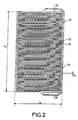
- Figure 2 illustrates a possible embodiment of a resistance according to the invention capable of replacing the resistance previous in a tube transmitter.
- This resistance is flat metallic of the printed circuit type. It therefore includes at least one support dielectric 21, for example in organic material, and a flat conductor 22, the two terminals of the resistor being electrically connected at the ends of the conductor 22.
- the support is for example an organic substrate 21 of epoxy or polyimide nature.
- the flat conductor 22 is bonded to the substrate 21 and then etched for example by chemical machining with iron perchloride according to conventional printed circuit technology.
- the thickness e is particularly low since the conductor 22 is obtained by chemical etching.
- the flat conductor has for example the shape of a coil.
- the latter comprises for example sections of rectilinear conductors in parallel, with the smallest possible space between two neighboring sections 23, 24. This minimum space is defined by the resistance to electrical breakdown between the two sections 23, 24.
- the ends of the coil end for example by two receiving areas to allow the wiring of the resistor with two connection wires.
- this flash outfit consists of in particular that the metallic conductor 22 does not reach temperatures which deteriorate the organic substrate 21.
- the temperature of the conductor 22 does not exceed a given temperature, for example of the order of 300 ° C.
- the mass of the flat conductor must be sufficiently large.
- the thickness of the latter being for example fixed, we then play on the width l and length L of the flat conductor to obtain the minimum mass which guarantees the maximum temperature during a flash.
- the resistance R being itself imposed, it is necessary to play on these two parameters l, L, for a given thickness e, so that the ratio between these last two defining the resistance R according to the previous relation (1) remains constant.
- the flat conductor 22 must have a resistivity p sufficient to obtain the resistance value R without requiring too long a length while having no parasitic self-induction effect.
- a conductive material which meets these requirements comprises a nickel alloy.
- a material which can be used is known under the designation NC15Fe according to the AFNOR standard.
- the length L T and the width l d of a resistance according to the invention are for example respectively around 75mm and 45mm, with a space e 1 between two neighboring sections of 0.3mm.
- the organic substrate 21 is by example arranged on a ceramic support, the latter being able moreover have the function of mechanical support, knowing that the small thickness possible organic substrate gives it a certain flexibility.
- the latter is by example covered with an insulating layer which can be of the same nature as the substrate 21.
- the thickness of the resistance may be less than two millimeters, possibly depending on the thickness of the ceramic support this thickness can be more important, but still of the order of a few millimeters.
- Figures 4 and 5 illustrate another embodiment of a resistance according to the invention.
- This embodiment also makes it possible to advantageously reduce the space occupied by the resistance.
- the previous embodiment shows resistance of thin and relatively small in area for high strength voltage, which can for example hold 35 kV for a continuous power of the order of a hundred watts, this surface may still be too important for some applications. This may in particular be the case if the mass of flat conductor, so its length and area must be increased to further reduce the heating temperature.
- the Figure 4 shows that the surface occupied by the resistor as illustrated by Figures 2 and 3 can be halved by folding the resistance over itself as illustrated in Figure 4, due to the flexibility of the components.
- FIG. 6 shows an embodiment of a resistance according to the invention with housing.
- the resistor therefore includes a housing 61 in which is for example fixed an assembly as illustrated by FIGS. 2 to 5.
- the case contains a resistive assembly folded around a ceramic support according to Figures 4 and 5.
- the housing 61 has for example the shape of a ramekin with flat bottom. It is ceramic, for example alumina, the shape of the housing being obtained by machining the ceramic before sintering.
- the box comprises for example fixing holes 62 in order to fix it in particular on a mechanical support, for example a radiator of a tube transmitter.
- connection wires 63, 64 are soldered to the reception areas 25, 26 to allow the driver to be electrically connected flat with the outside.
- the connection wires are for example fixed on the flat conductor 22 by a tin-silver solder (SnAg). Resistance fixed at the bottom of the case and the connection cables are covered with protective resin 65 which in particular avoids the use of a cover.
- the protective resin is hot poured into the housing then hardens.
- a machined ceramic case associated with a resin protection can be achieved economically.
- the embodiment of a resistance according to the invention presented relative to FIG. 2 comprises an organic substrate on which is fixed the flat conductor.
- Another example of realization of a resistance according to the invention can also be applied in the case where the substrate or support is not organic, the support can be in this case by example in ceramic.
- the flat conductor is fixed on the support by means organic glue. It is then necessary to prevent the flat conductor overheats to the point of damaging the organic glue.
- a resistance according to the invention has many advantages. Its printed circuit type structure allows very good reproducibility resistance values as well as operational reliability, especially with regard to drifts. It also presents the advantage of not depending on scarce sources of supply or random. All its constituent elements are indeed easy to supply, because essentially conventional. This therefore results in reliability supply. It is low cost, in particular because its components are not in themselves expensive on the one hand, and that the assembly of these elements by the conventional technique of the printed circuit and that ceramic machining are inexpensive techniques to implement on the other hand. Finally, a resistance according to the invention supports very high voltages, of the order of a few tens of kilovolts while occupying a very small volume. It is therefore very well suited for a tube transmitter, intended in particular for an airborne radar subjected to very restrictive congestion problems.
- the invention therefore allows a microwave tube transmitter equipped with a limiting resistor as described above relative to FIGS. 2 to 6 to gain operational reliability and supply and gain bulk.
- the resistance of limitation is then for example wired to the grid cathode the transmitter.
- two or more resistors can be wired in parallel or serial.
- a resistor according to the invention can also be wired to the tube collector.
- a resistance according to the invention has in particular been described to be used as a limiting resistor in a power transmitter with microwave tube. It can however be used for other applications that require similar performance, for example, from the point of view of the withstand as of the size or the cost.
Landscapes
- Engineering & Computer Science (AREA)
- Microelectronics & Electronic Packaging (AREA)
- Physics & Mathematics (AREA)
- Electromagnetism (AREA)
- Details Of Resistors (AREA)
- Crystals, And After-Treatments Of Crystals (AREA)
- Amplifiers (AREA)
- Emergency Protection Circuit Devices (AREA)
- Radar Systems Or Details Thereof (AREA)
Abstract
Description
- la figure 1, un exemple de réalisation d'une résistance haute tension selon l'art antérieur ;
- la figure 2, un exemple de réalisation d'une résistance haute tension selon l'invention ;
- la figure 3, par une vue en coupe, les couches constitutives d'un exemple de résistance selon l'invention ;
- la figure 4, un exemple de réalisation d'une résistance selon l'invention où une partie de ces éléments est repliée sur elle-même ;
- la figure 5, une vue en coupe du mode de réalisation précédent ;
- la figure 6, un exemple de réalisation d'une résistance selon l'invention pourvue d'un boítier.
- support en céramique 34 : de l'ordre d'un millimètre ;
- couche de colle 35 entre le support alumine et le premier substrat organique : 25 µm ;
- substrats organiques 21, 32 : 75 µm ;
- couches de colle 31, 33 entre les substrats organiques et le conducteur plat : 50 µm ;
- conducteur plat 22 : 100 µm.
Claims (17)
- Résistance haute tension, caractérisée en ce qu'elle comporte au moins un support (21) et un conducteur plat (22) de longueur L, de largeur ℓ et d'épaisseur e fixé sur le support et ayant une résistivité p donnée, la valeur R de résistance étant égale à ρL/ℓ e, les valeurs de la longueur L, de la largeur ℓ et de l'épaisseur e étant par ailleurs définies de façon à ce que le conducteur plat (22) présente une masse suffisante pour subir des flashs électriques sans dépasser une température donnée.
- Résistance selon la revendication 1, caractérisé en ce que le support (21) est un substrat organique.
- Résistance selon la revendication 1, caractérisé en ce que le conducteur (22) est fixé sur le support au moyen d'une colle organique.
- Résistance selon l'une quelconque des revendications précédentes, caractérisée en ce que le conducteur plat (22) a la forme d'un serpentin.
- Résistance selon la revendication 4, caractérisée en ce que le conducteur plat (22) comporte des tronçons rectilignes parallèles (23, 24).
- Résistance selon l'une quelconque des revendications précédentes, caractérisée en ce que le conducteur plat (22) comporte un alliage de nickel.
- Résistance selon l'une quelconque des revendications précédentes, caractérisée en ce que le conducteur plat (22) est recouvert d'une couche isolante (32).
- Résistance selon la revendication 7, caractérisée en ce que la couche isolante est un substrat organique.
- Résistance selon la revendication 2 et l'une quelconque des revendications 4 à 8, caractérisée en ce que le substrat organique est fixé sur un support en céramique (34).
- Résistance selon l'une quelconque des revendications 2 et 4 à 8 caractérisée en ce que la résistance est repliée sur elle-même.
- Résistance selon la revendication 10, caractérisée en ce que le substrat organique est fixé des deux côtés d'un support en céramique.
- Résistance selon l'une quelconque des revendications précédentes, caractérisé en ce qu'elle comporte des fils de connexions dont les extrémités sont brasées sur des plages d'accueil (25, 26) du conducteur plat (22).
- Résistance selon l'une quelconque des revendications précédentes, caractérisée en ce qu'elle est fixée sur le fond d'un boítier en céramique (61).
- Résistance selon la revendication 13, caractérisée en ce que la résistance est protégée par une résine coulée dans le boítier.
- Emetteur à tube hyperfréquence, caractérisé en ce qu'il est équipé d'une ou plusieurs résistances de limitation selon l'une quelconque des revendications précédentes.
- Emetteur selon la revendication 15, caractérisé en ce que la ou les résistances sont câblées sur la cathode de la grille du tube.
- Emetteur selon la revendication 15, caractérisé en ce que la ou les résistances sont câblées sur le collecteur du tube.
Applications Claiming Priority (2)
| Application Number | Priority Date | Filing Date | Title |
|---|---|---|---|
| FR0001541 | 2000-02-08 | ||
| FR0001541A FR2804788B1 (fr) | 2000-02-08 | 2000-02-08 | Resistance haute tension, notamment de limitation de courant dans un emetteur a tube hyperfrequence a onde progressive |
Publications (2)
| Publication Number | Publication Date |
|---|---|
| EP1126479A1 true EP1126479A1 (fr) | 2001-08-22 |
| EP1126479B1 EP1126479B1 (fr) | 2006-09-27 |
Family
ID=8846757
Family Applications (1)
| Application Number | Title | Priority Date | Filing Date |
|---|---|---|---|
| EP01400289A Expired - Lifetime EP1126479B1 (fr) | 2000-02-08 | 2001-02-06 | Résistance haute tension, notamment de limitation de courant dans un émetteur à tube hyperfréquence à onde progressive |
Country Status (6)
| Country | Link |
|---|---|
| US (1) | US20010020890A1 (fr) |
| EP (1) | EP1126479B1 (fr) |
| AT (1) | ATE341087T1 (fr) |
| CA (1) | CA2334423A1 (fr) |
| DE (1) | DE60123303D1 (fr) |
| FR (1) | FR2804788B1 (fr) |
Citations (5)
| Publication number | Priority date | Publication date | Assignee | Title |
|---|---|---|---|---|
| US3654580A (en) * | 1969-03-14 | 1972-04-04 | Sanders Associates Inc | Resistor structure |
| US3824521A (en) * | 1973-09-24 | 1974-07-16 | Tdk Electronics Co Ltd | Resistor |
| GB2032460A (en) * | 1978-09-13 | 1980-05-08 | Yates Industries | Surface Treated Electrically Resistive Metal Foil for Production of Printed Electrical Resistors |
| US5118991A (en) * | 1989-09-09 | 1992-06-02 | Ptr Prazisionstechnik Gmbh | Electron beam generator for an electron gun |
| US5548268A (en) * | 1993-10-06 | 1996-08-20 | Collins; Franklyn M. | Fine-line thick film resistors and resistor networks and method of making same |
-
2000
- 2000-02-08 FR FR0001541A patent/FR2804788B1/fr not_active Expired - Fee Related
-
2001
- 2001-02-02 CA CA002334423A patent/CA2334423A1/fr not_active Abandoned
- 2001-02-06 EP EP01400289A patent/EP1126479B1/fr not_active Expired - Lifetime
- 2001-02-06 US US09/776,688 patent/US20010020890A1/en not_active Abandoned
- 2001-02-06 DE DE60123303T patent/DE60123303D1/de not_active Expired - Lifetime
- 2001-02-06 AT AT01400289T patent/ATE341087T1/de not_active IP Right Cessation
Patent Citations (5)
| Publication number | Priority date | Publication date | Assignee | Title |
|---|---|---|---|---|
| US3654580A (en) * | 1969-03-14 | 1972-04-04 | Sanders Associates Inc | Resistor structure |
| US3824521A (en) * | 1973-09-24 | 1974-07-16 | Tdk Electronics Co Ltd | Resistor |
| GB2032460A (en) * | 1978-09-13 | 1980-05-08 | Yates Industries | Surface Treated Electrically Resistive Metal Foil for Production of Printed Electrical Resistors |
| US5118991A (en) * | 1989-09-09 | 1992-06-02 | Ptr Prazisionstechnik Gmbh | Electron beam generator for an electron gun |
| US5548268A (en) * | 1993-10-06 | 1996-08-20 | Collins; Franklyn M. | Fine-line thick film resistors and resistor networks and method of making same |
Also Published As
| Publication number | Publication date |
|---|---|
| DE60123303D1 (de) | 2006-11-09 |
| ATE341087T1 (de) | 2006-10-15 |
| CA2334423A1 (fr) | 2001-08-08 |
| US20010020890A1 (en) | 2001-09-13 |
| EP1126479B1 (fr) | 2006-09-27 |
| FR2804788A1 (fr) | 2001-08-10 |
| FR2804788B1 (fr) | 2002-09-20 |
Similar Documents
| Publication | Publication Date | Title |
|---|---|---|
| EP2217933B1 (fr) | Sonde aeronautique a rechauffeur integre | |
| FR2690003A1 (fr) | Résistance pastille à couche métallique. | |
| FR2813440A1 (fr) | Dispositif a semiconducteur pour la commande d'energie electrique | |
| FR2760931A1 (fr) | Ensemble capteur-dispositif de chauffage | |
| FR2782597A1 (fr) | Module d'alimentation electrique | |
| EP0030186A1 (fr) | Shunt de mesure à compensation de tension d'erreur induite | |
| EP1141887B1 (fr) | Procede de fabrication de carte a puce sans contact | |
| WO2018055276A1 (fr) | Structure de détection de rayonnements électromagnétiques de type bolomètre et procédé de fabrication d'une telle structure | |
| EP0044756A2 (fr) | Résistance électrique chauffante et tête d'imprimante thermique comportant de telles résistances chauffantes | |
| EP1126479B1 (fr) | Résistance haute tension, notamment de limitation de courant dans un émetteur à tube hyperfréquence à onde progressive | |
| FR2777385A1 (fr) | Eclateur vertical pour circuits microelectroniques et son procede de fabrication | |
| EP0779775B1 (fr) | Assemblage électronique à drain thermique, notamment pour transformateur haute tension de lampe à décharge de projecteur de véhicule automobile | |
| EP1979938B1 (fr) | Module electronique et procede d'assemblage d'un tel module | |
| FR3026226A1 (fr) | Plaque de circuit | |
| WO2003096414A2 (fr) | Assemblage de composants de puissance sur un circuit imprime ainsi qu'un procede d'un tel assemblage | |
| EP2134147B1 (fr) | Procédé de soudure et de positionnement d'un circuit intégré sur un substrat et assemblage réalisé par ce procédé | |
| WO2022128457A1 (fr) | Module thermoélectrique et échangeur thermique associé | |
| FR2631154A1 (fr) | Resistance de puissance electrique | |
| EP0855722B1 (fr) | Résistance à forte dissipation de puissance et/ou d'énergie et son procédé de fabrication | |
| EP3731612B1 (fr) | Dispositif de commande a refroidissement optimise pour actionneur electrique | |
| EP0637826B1 (fr) | Composant résistif de puissance, avec dispositif d'application sous pression sur un dissipateur thermique | |
| FR3066858B1 (fr) | Procede pour minimiser une distorsion d'un signal dans un circuit radiofrequence | |
| EP0391751A2 (fr) | Resistance shunt | |
| EP4295400A1 (fr) | Module électronique de puissance | |
| JP2006024933A (ja) | 抵抗性熱発生素子を有する電気装置 |
Legal Events
| Date | Code | Title | Description |
|---|---|---|---|
| PUAI | Public reference made under article 153(3) epc to a published international application that has entered the european phase |
Free format text: ORIGINAL CODE: 0009012 |
|
| AK | Designated contracting states |
Kind code of ref document: A1 Designated state(s): AT BE CH CY DE DK ES FI FR GB GR IE IT LI LU MC NL PT SE TR |
|
| AX | Request for extension of the european patent |
Free format text: AL;LT;LV;MK;RO;SI |
|
| RAP1 | Party data changed (applicant data changed or rights of an application transferred) |
Owner name: THALES |
|
| 17P | Request for examination filed |
Effective date: 20020213 |
|
| AKX | Designation fees paid |
Free format text: AT BE CH CY DE DK ES FI FR GB GR IE IT LI LU MC NL PT SE TR |
|
| GRAP | Despatch of communication of intention to grant a patent |
Free format text: ORIGINAL CODE: EPIDOSNIGR1 |
|
| GRAS | Grant fee paid |
Free format text: ORIGINAL CODE: EPIDOSNIGR3 |
|
| GRAA | (expected) grant |
Free format text: ORIGINAL CODE: 0009210 |
|
| AK | Designated contracting states |
Kind code of ref document: B1 Designated state(s): AT BE CH CY DE DK ES FI FR GB GR IE IT LI LU MC NL PT SE TR |
|
| PG25 | Lapsed in a contracting state [announced via postgrant information from national office to epo] |
Ref country code: IT Free format text: LAPSE BECAUSE OF FAILURE TO SUBMIT A TRANSLATION OF THE DESCRIPTION OR TO PAY THE FEE WITHIN THE PRESCRIBED TIME-LIMIT;WARNING: LAPSES OF ITALIAN PATENTS WITH EFFECTIVE DATE BEFORE 2007 MAY HAVE OCCURRED AT ANY TIME BEFORE 2007. THE CORRECT EFFECTIVE DATE MAY BE DIFFERENT FROM THE ONE RECORDED. Effective date: 20060927 Ref country code: AT Free format text: LAPSE BECAUSE OF FAILURE TO SUBMIT A TRANSLATION OF THE DESCRIPTION OR TO PAY THE FEE WITHIN THE PRESCRIBED TIME-LIMIT Effective date: 20060927 Ref country code: FI Free format text: LAPSE BECAUSE OF FAILURE TO SUBMIT A TRANSLATION OF THE DESCRIPTION OR TO PAY THE FEE WITHIN THE PRESCRIBED TIME-LIMIT Effective date: 20060927 Ref country code: NL Free format text: LAPSE BECAUSE OF FAILURE TO SUBMIT A TRANSLATION OF THE DESCRIPTION OR TO PAY THE FEE WITHIN THE PRESCRIBED TIME-LIMIT Effective date: 20060927 Ref country code: IE Free format text: LAPSE BECAUSE OF FAILURE TO SUBMIT A TRANSLATION OF THE DESCRIPTION OR TO PAY THE FEE WITHIN THE PRESCRIBED TIME-LIMIT Effective date: 20060927 |
|
| REG | Reference to a national code |
Ref country code: GB Ref legal event code: FG4D Free format text: NOT ENGLISH |
|
| REG | Reference to a national code |
Ref country code: CH Ref legal event code: EP |
|
| REG | Reference to a national code |
Ref country code: IE Ref legal event code: FG4D Free format text: LANGUAGE OF EP DOCUMENT: FRENCH |
|
| REF | Corresponds to: |
Ref document number: 60123303 Country of ref document: DE Date of ref document: 20061109 Kind code of ref document: P |
|
| PG25 | Lapsed in a contracting state [announced via postgrant information from national office to epo] |
Ref country code: DK Free format text: LAPSE BECAUSE OF FAILURE TO SUBMIT A TRANSLATION OF THE DESCRIPTION OR TO PAY THE FEE WITHIN THE PRESCRIBED TIME-LIMIT Effective date: 20061227 Ref country code: SE Free format text: LAPSE BECAUSE OF FAILURE TO SUBMIT A TRANSLATION OF THE DESCRIPTION OR TO PAY THE FEE WITHIN THE PRESCRIBED TIME-LIMIT Effective date: 20061227 |
|
| PG25 | Lapsed in a contracting state [announced via postgrant information from national office to epo] |
Ref country code: DE Free format text: LAPSE BECAUSE OF FAILURE TO SUBMIT A TRANSLATION OF THE DESCRIPTION OR TO PAY THE FEE WITHIN THE PRESCRIBED TIME-LIMIT Effective date: 20061228 |
|
| PG25 | Lapsed in a contracting state [announced via postgrant information from national office to epo] |
Ref country code: ES Free format text: LAPSE BECAUSE OF FAILURE TO SUBMIT A TRANSLATION OF THE DESCRIPTION OR TO PAY THE FEE WITHIN THE PRESCRIBED TIME-LIMIT Effective date: 20070107 |
|
| GBT | Gb: translation of ep patent filed (gb section 77(6)(a)/1977) |
Effective date: 20070109 |
|
| PG25 | Lapsed in a contracting state [announced via postgrant information from national office to epo] |
Ref country code: LI Free format text: LAPSE BECAUSE OF NON-PAYMENT OF DUE FEES Effective date: 20070228 Ref country code: CH Free format text: LAPSE BECAUSE OF NON-PAYMENT OF DUE FEES Effective date: 20070228 Ref country code: MC Free format text: LAPSE BECAUSE OF NON-PAYMENT OF DUE FEES Effective date: 20070228 |
|
| NLV1 | Nl: lapsed or annulled due to failure to fulfill the requirements of art. 29p and 29m of the patents act | ||
| PG25 | Lapsed in a contracting state [announced via postgrant information from national office to epo] |
Ref country code: PT Free format text: LAPSE BECAUSE OF FAILURE TO SUBMIT A TRANSLATION OF THE DESCRIPTION OR TO PAY THE FEE WITHIN THE PRESCRIBED TIME-LIMIT Effective date: 20070313 |
|
| REG | Reference to a national code |
Ref country code: IE Ref legal event code: FD4D |
|
| PLBE | No opposition filed within time limit |
Free format text: ORIGINAL CODE: 0009261 |
|
| STAA | Information on the status of an ep patent application or granted ep patent |
Free format text: STATUS: NO OPPOSITION FILED WITHIN TIME LIMIT |
|
| 26N | No opposition filed |
Effective date: 20070628 |
|
| REG | Reference to a national code |
Ref country code: CH Ref legal event code: PL |
|
| REG | Reference to a national code |
Ref country code: FR Ref legal event code: ST Effective date: 20071030 |
|
| BERE | Be: lapsed |
Owner name: THALES Effective date: 20070228 |
|
| PG25 | Lapsed in a contracting state [announced via postgrant information from national office to epo] |
Ref country code: BE Free format text: LAPSE BECAUSE OF NON-PAYMENT OF DUE FEES Effective date: 20070228 |
|
| PG25 | Lapsed in a contracting state [announced via postgrant information from national office to epo] |
Ref country code: GR Free format text: LAPSE BECAUSE OF FAILURE TO SUBMIT A TRANSLATION OF THE DESCRIPTION OR TO PAY THE FEE WITHIN THE PRESCRIBED TIME-LIMIT Effective date: 20061228 Ref country code: FR Free format text: LAPSE BECAUSE OF NON-PAYMENT OF DUE FEES Effective date: 20070228 |
|
| PG25 | Lapsed in a contracting state [announced via postgrant information from national office to epo] |
Ref country code: CY Free format text: LAPSE BECAUSE OF FAILURE TO SUBMIT A TRANSLATION OF THE DESCRIPTION OR TO PAY THE FEE WITHIN THE PRESCRIBED TIME-LIMIT Effective date: 20060927 Ref country code: LU Free format text: LAPSE BECAUSE OF NON-PAYMENT OF DUE FEES Effective date: 20070206 |
|
| PG25 | Lapsed in a contracting state [announced via postgrant information from national office to epo] |
Ref country code: TR Free format text: LAPSE BECAUSE OF FAILURE TO SUBMIT A TRANSLATION OF THE DESCRIPTION OR TO PAY THE FEE WITHIN THE PRESCRIBED TIME-LIMIT Effective date: 20060927 |
|
| PGFP | Annual fee paid to national office [announced via postgrant information from national office to epo] |
Ref country code: IT Payment date: 20160222 Year of fee payment: 16 |
|
| PGFP | Annual fee paid to national office [announced via postgrant information from national office to epo] |
Ref country code: GB Payment date: 20160203 Year of fee payment: 16 |
|
| GBPC | Gb: european patent ceased through non-payment of renewal fee |
Effective date: 20170206 |
|
| PG25 | Lapsed in a contracting state [announced via postgrant information from national office to epo] |
Ref country code: GB Free format text: LAPSE BECAUSE OF NON-PAYMENT OF DUE FEES Effective date: 20170206 Ref country code: IT Free format text: LAPSE BECAUSE OF NON-PAYMENT OF DUE FEES Effective date: 20170206 |