EP1126351A1 - Schaltungsanordnung zur Konstantspannungserzeugung - Google Patents
Schaltungsanordnung zur Konstantspannungserzeugung Download PDFInfo
- Publication number
- EP1126351A1 EP1126351A1 EP01101805A EP01101805A EP1126351A1 EP 1126351 A1 EP1126351 A1 EP 1126351A1 EP 01101805 A EP01101805 A EP 01101805A EP 01101805 A EP01101805 A EP 01101805A EP 1126351 A1 EP1126351 A1 EP 1126351A1
- Authority
- EP
- European Patent Office
- Prior art keywords
- transistor
- emitter
- connections
- circuit
- current
- Prior art date
- Legal status (The legal status is an assumption and is not a legal conclusion. Google has not performed a legal analysis and makes no representation as to the accuracy of the status listed.)
- Granted
Links
Images

Classifications
-
- G—PHYSICS
- G05—CONTROLLING; REGULATING
- G05F—SYSTEMS FOR REGULATING ELECTRIC OR MAGNETIC VARIABLES
- G05F3/00—Non-retroactive systems for regulating electric variables by using an uncontrolled element, or an uncontrolled combination of elements, such element or such combination having self-regulating properties
- G05F3/02—Regulating voltage or current
- G05F3/08—Regulating voltage or current wherein the variable is DC
- G05F3/10—Regulating voltage or current wherein the variable is DC using uncontrolled devices with non-linear characteristics
- G05F3/16—Regulating voltage or current wherein the variable is DC using uncontrolled devices with non-linear characteristics being semiconductor devices
- G05F3/20—Regulating voltage or current wherein the variable is DC using uncontrolled devices with non-linear characteristics being semiconductor devices using diode- transistor combinations
- G05F3/30—Regulators using the difference between the base-emitter voltages of two bipolar transistors operating at different current densities
Definitions
- the invention relates to a circuit arrangement for generation of constant voltages and / or constant currents after Bandgap principle (bandgap principle), in which the flow voltages two P-N junctions to generate a reference voltage are used, according to the preamble of Claim 1.
- Bandgap principle Bandgap principle
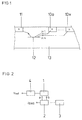
- Another problem can arise, for example, according to FIG. 1 with a barrier technology insulated mixing technology on one p-substrate 13 result.
- This is done with a polarity reversal on a DMOS power transistor (reverse operation) from a n-type drain connection 11 and the p-type substrate 13 are formed Diode conductive, and those injected into the substrate 13 Charge carriers form the emitter current of a parasitic bipolar npn area transistor 12.
- All epitaxial n wells 10a, ... 10x (for example BJT collectors) of the circuit 12 potential collectors for this transistor those in reverse operation of the DMOS power transistor collector currents Icl, .. Icx can be deducted. This can cause sensitive other circuit parts with high-resistance connected n-wells, such as one Circuit arrangement of the type mentioned at the outset based on the bandgap principle, be impaired in their function or even fail completely.
- the invention is therefore based on the object of a circuit arrangement to create a temperature range within and constant voltage independent of the operating voltage and / or a constant current with a bandgap reference generated and particularly insensitive to Influences of the reverse operation described above.
- an output buffer / driver is provided in particular, with which the reference voltage is divided and applied with low resistance an exit is led.
- the circuit arrangement preferably comprises a comparator with a current mirror circuit with which the emitter currents of the first and second transistor and the reference current be regulated in an equilibrium state in which these currents are essentially the same.
- an actuator with a starting circuit provided to act on the comparator, the has a third transistor with which a voltage or Current difference at the emitter connections of the first and second transistor by driving a fourth and fifth Transistor is compensated in the comparator.
- the embodiment according to the invention comprises a bandgap circuit 1 for generating a reference voltage according to the bandgap principle, based on a positive supply voltage Vdd is related to an output buffer / driver 4, whose input connects to the output of the bandgap circuit 1 is connected and at its output an output reference voltage Vref is present, a current and voltage comparator 2, which is insensitive to reverse current and via a first and a second terminal A, B with the bandgap circuit 1 is connected, and an actuator 3 with start circuit, the applied to the comparator 2.
- the output buffer / driver 4 is used by the bandgap circuit 1 generated reference voltage to almost any Values (for example ⁇ 1.26 volts) divided and low-resistance at the output made available.
- the comparator 2 also controls With the help of the actuator 3, the bandgap circuit 1, the condition to be fulfilled for the regulated state Equality of the voltages at the two terminals A, B and the equality of the currents I1, I2 through these terminals is.
- FIG. 3 shows an overall circuit diagram of the preferred embodiment, these components each with dashed lines Lines are delimited.
- the bandgap circuit 1 comprises a first and a second bipolar npn transistor T1, T2, whose base connections over a first resistor R1 are connected together.
- the Collector connections are connected to a positive supply voltage Vdd on, while the emitter connection of the first Transistor T1 to the first terminal A and the emitter connection of the second transistor T2 to the second terminal B. is.
- the base terminal of the first transistor is T1 finally via a second resistor R2 with the supply voltage Vdd connected.
- the comparator 2 comprises a fourth and a fifth bipolar pnp transistor T4, T5, the base connections of which are connected to one another, the emitter of the fourth transistor T4 via the second terminal B to the emitter of the second transistor T2 and the emitter of the fifth transistor T5 the first terminal A is connected to the emitter of the first transistor T1.
- the collector of the fifth transistor T5 is connected via a first (for example MOSFET) transistor M1 to ground and to a gate of this transistor M1.
- the collector of the fourth transistor T4 is connected to ground via a third MOSFET transistor M3.
- a second MOSFET transistor M2 is provided which allows a reference current Iref to flow from the base of the second transistor T2 to ground.
- a temperature-independent bias current I BIAS can be generated to ground via a tenth MOSFET transistor M10 and can be coupled out if necessary.
- the circuit arrangement can thus additionally serve as a generator for a temperature-compensated bias current I BIAS for the chip in question and in this way comprises an inherent "auto-biasing".
- the base connections of the MOSFET transistors M1, M2, M3, M10 are connected to one another.
- the actuator 3 comprises a third bipolar npn transistor T3, whose collector with the positive supply voltage Vdd and its emitter with the interconnected Base connections of the fourth and fifth transistor T4, T5 and a third resistor R3 connected to ground is. Between the supply voltage Vdd and ground are a fourth and a seventh MOSFET transistor M4, M7 in Series connected, between which the base of the third Transistor T3 is.
- the gate of the fourth MOSFET transistor M4 is the gate of the fourth transistor T4 of the seventh MOSFET transistor M7 has an eighth with the gate MOSFET transistor M8 connected in series with one ninth MOSFET transistor M9 between the supply voltage Vdd and mass is.
- the gate of the seventh and eighth MOSFET transistors M7, M8 is between the eighth and ninth MOSFET transistor M8, M9 switched.
- the gate of the ninth MOSFET transistor M9 is with the interconnected gate terminals of the first, second, third and tenth MOSFET transistors M1, M2, M3, M10 connected.
- the output buffer / Driver 4 realizes a sixth bipolar pnp transistor T6 comprises whose emitter is connected in series a fourth and fifth resistor R4, R5 with the Supply voltage Vdd and its collector via a fifth MOSFET transistor M5 is connected to ground. The emitter is also present via a sixth MOSFET transistor M6 Ground whose gate is connected to the collector of the sixth transistor T6 is connected.
- the base of the fifth MOSFET transistor M5 is in turn with the interconnected gate connections of the first, second, third, ninth and tenth MOSFET transistors M1, M2, M3, M9, M10 connected.
- the reference voltage Vref is at the through the fourth and fifth resistance R4, R5 tapped voltage divider.
- An essential core of the invention is the implementation of the bandgap principle in the bandgap circuit 1, which can also be used independently, that is to say without the circuit parts 2 to 4. However, it is particularly suitable for use in combination with the comparator 2, as a result of which the overall circuit is insensitive to the reverse currents mentioned at the beginning. Furthermore, with the current-determining first resistor R1, the temperature response of the difference between the two base emitter voltages of T1 and T2 dU BE is compensated, so that the reference current Iref is independent of temperature.
- the circuit is self-sufficient, so that there are two possible working points, on the one hand a desired and on the other hand such a working point, where the reference current Iref is zero and the reference voltage Vref is equal to the positive supply voltage Vdd is.
- the known circuits with this property The starting circuit is often difficult to implement integrated in the actuator 3 without an essential to require additional effort.
- the reference voltage results from the sum of the voltage drop across the second resistor R2 generated by the reference current Iref and the voltage U BE across the base-emitter diode of the first transistor T1.
- the reference voltage Vref can be tapped at the first terminal A and relates to the positive supply voltage Vdd.
- the comparator 2 controls in interaction with the actuator 3 the bandgap circuit 1 always on this state of equilibrium from which the reference current Iref is equal to the first and the second current I1, I2 (emitter current of the first or second transistor T1, T2) through the first and second terminal A, B is.
- This current condition is determined by the first to third MOSFET transistor M1, M2, M3 formed Current mirror circuit realized.
- the current mirror upstream pnp transistors T4, T5 has a potential difference a current difference directly at terminals A, B result and is therefore also corrected.
- the third resistor R3 forms a current sink for the third transistor T3 and also acts as a starting resistor, by disconnecting the base connections of the fourth to sixth transistor T4, T5, T6 pulls to ground and so excludes the undesired working point.
- the optional output buffer / driver 4 drives the sixth Transistor T6 with a base potential and an emitter current, that is identical to those on the fourth and fifth transistor T4, T5.
- the emitter potential corresponds the potential at the first and second terminals A, B and thus the reference voltage Vref.
- the requirement of the identical Emitter current is through the fifth and sixth MOSFET transistor M5, M6 fulfilled. If the emitter and thus the collector current through the sixth transistor T6 increases, the potential at the fifth MOSFET transistor also increases M5, so that the fourth MOSFET transistor M4 is turned on and takes over the excess electricity.
Landscapes
- Engineering & Computer Science (AREA)
- Microelectronics & Electronic Packaging (AREA)
- Physics & Mathematics (AREA)
- Power Engineering (AREA)
- Nonlinear Science (AREA)
- Electromagnetism (AREA)
- General Physics & Mathematics (AREA)
- Radar, Positioning & Navigation (AREA)
- Automation & Control Theory (AREA)
- Control Of Electrical Variables (AREA)
Abstract
Description
Claims (6)
- Schaltungsanordnung zur Erzeugung von Konstantspannungen und / oder Konstantströmen nach dem Bandgap-Prinzip,
gekennzeichnet durch
einen ersten und einen zweiten Transistor (T1, T2), deren Basisanschlüsse über einen ersten Widerstand (R1) miteinander verbunden sind und deren Kollektoranschlüsse an einer Versorgungsspannung (Vdd) anliegen, sowie einen zweiten Widerstand (R2), der zwischen den Basisanschluss des ersten Transistors (T1) und die Versorgungsspannung (Vdd) geschaltet ist, so dass durch die Differenz der Basis-Emitter-Spannungen an den Transistoren (T1, T2) ein durch den ersten und zweiten Widerstand (R1, R2) nach Masse fließender Referenzstrom (Iref) erzeugt wird, und eine auf die Versorgungsspannung (Vdd) bezogene Referenzspannung (Vref) an dem Emitter des ersten Transistors (T1) abgreifbar ist. - Schaltungsanordnung nach Anspruch 1,
gekennzeichnet durch
einen Ausgangspuffer / Treiber (4), mit dem die Referenzspannung geteilt und niederohmig an einen Ausgang geführt wird. - Schaltungsanordnung nach Anspruch 1 oder 2,
gekennzeichnet durch
einen Komparator (2) mit einer Stromspiegelschaltung (M1, M2, M3), mit der die Emitterströme (I1, I2) des ersten und zweiten Transistors (T1, T2) sowie der Referenzstrom (Iref) in einen Gleichgewichtszustand geregelt werden, in dem diese Ströme im wesentlichen gleich sind. - Schaltungsanordnung nach Anspruch 3,
dadurch gekennzeichnet, dass
der Komparator (2) einen vierten und einen fünften Transistor (T4, T5) aufweist, deren Gateanschlüsse miteinander und deren Emitteranschlüsse mit den Emitteranschlüssen des ersten bzw. zweiten Transistors (T1, T2) verbunden sind, so dass eine Spannungsdifferenz an diesen Anschlüssen eine Stromdifferenz zur Folge hat, die mit der Stromspiegelschaltung (M1, M2, M3) ausgeregelt wird. - Schaltungsanordnung nach Anspruch 3 oder 4,
gekennzeichnet durch
einen zehnten, durch die Stromspiegelschaltung angesteuerten Transistor (M10), zur Erzeugung eines temperaturunabhängigen Bias-Stroms (IBIAS). - Schaltungsanordnung nach einem der Ansprüche 3 bis 5,
gekennzeichnet durch
ein Stellglied (3) mit einer Startschaltung zur Beaufschlagung des Komparators (2), das einen dritten Transistor (T3) aufweist, mit dem eine Spannungs- oder Stromdifferenz an den Emitteranschlüssen des ersten und zweiten Transistors (T1, T2) durch Ansteuerung des vierten und fünften Transistors (T4, T5) ausgeregelt wird.
Applications Claiming Priority (2)
| Application Number | Priority Date | Filing Date | Title |
|---|---|---|---|
| DE2000106950 DE10006950C1 (de) | 2000-02-16 | 2000-02-16 | Schaltungsanordnung zur Konstantspannungs- und / oder Konstantstromerzeugung |
| DE10006950 | 2000-02-16 |
Publications (2)
| Publication Number | Publication Date |
|---|---|
| EP1126351A1 true EP1126351A1 (de) | 2001-08-22 |
| EP1126351B1 EP1126351B1 (de) | 2007-03-28 |
Family
ID=7631122
Family Applications (1)
| Application Number | Title | Priority Date | Filing Date |
|---|---|---|---|
| EP20010101805 Expired - Lifetime EP1126351B1 (de) | 2000-02-16 | 2001-01-26 | Schaltungsanordnung zur Konstantspannungserzeugung |
Country Status (2)
| Country | Link |
|---|---|
| EP (1) | EP1126351B1 (de) |
| DE (2) | DE10006950C1 (de) |
Cited By (1)
| Publication number | Priority date | Publication date | Assignee | Title |
|---|---|---|---|---|
| CN103699171A (zh) * | 2012-09-27 | 2014-04-02 | 无锡华润矽科微电子有限公司 | 具有高稳定性的能隙基准电流电路结构 |
Citations (3)
| Publication number | Priority date | Publication date | Assignee | Title |
|---|---|---|---|---|
| US4348633A (en) * | 1981-06-22 | 1982-09-07 | Motorola, Inc. | Bandgap voltage regulator having low output impedance and wide bandwidth |
| EP0329247A1 (de) * | 1988-02-19 | 1989-08-23 | Koninklijke Philips Electronics N.V. | Bandabstand-Referenzspannungsschaltung |
| EP0680048A1 (de) * | 1994-04-29 | 1995-11-02 | STMicroelectronics, Inc. | Bandabstands-Referenzschaltung |
-
2000
- 2000-02-16 DE DE2000106950 patent/DE10006950C1/de not_active Expired - Fee Related
-
2001
- 2001-01-26 DE DE50112251T patent/DE50112251D1/de not_active Expired - Fee Related
- 2001-01-26 EP EP20010101805 patent/EP1126351B1/de not_active Expired - Lifetime
Patent Citations (3)
| Publication number | Priority date | Publication date | Assignee | Title |
|---|---|---|---|---|
| US4348633A (en) * | 1981-06-22 | 1982-09-07 | Motorola, Inc. | Bandgap voltage regulator having low output impedance and wide bandwidth |
| EP0329247A1 (de) * | 1988-02-19 | 1989-08-23 | Koninklijke Philips Electronics N.V. | Bandabstand-Referenzspannungsschaltung |
| EP0680048A1 (de) * | 1994-04-29 | 1995-11-02 | STMicroelectronics, Inc. | Bandabstands-Referenzschaltung |
Cited By (2)
| Publication number | Priority date | Publication date | Assignee | Title |
|---|---|---|---|---|
| CN103699171A (zh) * | 2012-09-27 | 2014-04-02 | 无锡华润矽科微电子有限公司 | 具有高稳定性的能隙基准电流电路结构 |
| CN103699171B (zh) * | 2012-09-27 | 2015-10-28 | 无锡华润矽科微电子有限公司 | 具有高稳定性的能隙基准电流电路结构 |
Also Published As
| Publication number | Publication date |
|---|---|
| DE10006950C1 (de) | 2002-01-24 |
| EP1126351B1 (de) | 2007-03-28 |
| DE50112251D1 (de) | 2007-05-10 |
Similar Documents
| Publication | Publication Date | Title |
|---|---|---|
| DE69323818T2 (de) | Vorrichtung zur Erzeugung einer MOS temperaturkompensierten Referenzspannung für niedrige Spannungen und grosse Betriebsspannungsbereiche | |
| DE69224833T2 (de) | Leistungs-mosfet-treiber mit reduzierung des querstroms | |
| DE69634711T2 (de) | VBB-Referenz für spannungsgepümptes Substrat | |
| DE69530905T2 (de) | Schaltung und Verfahren zur Spannungsregelung | |
| DE69122844T2 (de) | Stromquelle mit einstellbaren Temperaturschwankungen | |
| DE19927007B4 (de) | Bandlücken-Bezugsspannung- Erzeugungsschaltung | |
| DE4037206A1 (de) | Quellspannungssteuerschaltkreis | |
| EP0508327A2 (de) | CMOS-Bandabstands-Referenzschaltung | |
| DE69423121T2 (de) | Temperaturkompensierter Spannungsregler | |
| EP0360887B1 (de) | CMOS-Spannungsreferenz | |
| DE2508226A1 (de) | Stromstabilisierungsschaltung | |
| DE69213213T2 (de) | Genauer MOS-Schwellenspannungsgenerator | |
| EP0637874B1 (de) | MOS-Schaltstufe | |
| EP0174473B1 (de) | Monolitisch integrierte Leistungsendstufe | |
| EP1523703A1 (de) | Bandabstands-referenzschaltung | |
| DE112022001961T5 (de) | Schaltung zum erzeugen einer stabilisierten spannung und halbleiterbauelement | |
| DE19821906C1 (de) | Klemmschaltung | |
| DE10047620B4 (de) | Schaltung zum Erzeugen einer Referenzspannung auf einem Halbleiterchip | |
| EP1126351B1 (de) | Schaltungsanordnung zur Konstantspannungserzeugung | |
| DE2607892A1 (de) | Transistordifferentialverstaerker | |
| DE112021001123T5 (de) | Klammerschaltung | |
| DE10053374C2 (de) | Bipolarer Komparator | |
| DE4329865C2 (de) | Schaltungsanordnung zur Einstellung des Querstroms einer Gegentaktendstufe | |
| DE102007059356B4 (de) | Stromspiegelanordnung und Verfahren zum Einschalten eines Stromes | |
| DE102005033434A1 (de) | Referenzspannungserzeugungsschaltung zur Erzeugung kleiner Referenzspannungen |
Legal Events
| Date | Code | Title | Description |
|---|---|---|---|
| PUAI | Public reference made under article 153(3) epc to a published international application that has entered the european phase |
Free format text: ORIGINAL CODE: 0009012 |
|
| AK | Designated contracting states |
Kind code of ref document: A1 Designated state(s): AT BE CH CY DE DK ES FI FR GB GR IE IT LI LU MC NL PT SE TR Kind code of ref document: A1 Designated state(s): DE FR GB IT |
|
| AX | Request for extension of the european patent |
Free format text: AL;LT;LV;MK;RO;SI |
|
| 17P | Request for examination filed |
Effective date: 20010719 |
|
| AKX | Designation fees paid |
Free format text: DE FR GB IT |
|
| 17Q | First examination report despatched |
Effective date: 20020425 |
|
| RIN1 | Information on inventor provided before grant (corrected) |
Inventor name: HORN, WOLFGANG |
|
| GRAP | Despatch of communication of intention to grant a patent |
Free format text: ORIGINAL CODE: EPIDOSNIGR1 |
|
| GRAS | Grant fee paid |
Free format text: ORIGINAL CODE: EPIDOSNIGR3 |
|
| GRAA | (expected) grant |
Free format text: ORIGINAL CODE: 0009210 |
|
| AK | Designated contracting states |
Kind code of ref document: B1 Designated state(s): DE FR GB IT |
|
| REG | Reference to a national code |
Ref country code: GB Ref legal event code: FG4D Free format text: NOT ENGLISH |
|
| REF | Corresponds to: |
Ref document number: 50112251 Country of ref document: DE Date of ref document: 20070510 Kind code of ref document: P |
|
| GBV | Gb: ep patent (uk) treated as always having been void in accordance with gb section 77(7)/1977 [no translation filed] |
Effective date: 20070328 |
|
| EN | Fr: translation not filed | ||
| PLBE | No opposition filed within time limit |
Free format text: ORIGINAL CODE: 0009261 |
|
| STAA | Information on the status of an ep patent application or granted ep patent |
Free format text: STATUS: NO OPPOSITION FILED WITHIN TIME LIMIT |
|
| 26N | No opposition filed |
Effective date: 20080102 |
|
| PG25 | Lapsed in a contracting state [announced via postgrant information from national office to epo] |
Ref country code: IT Free format text: LAPSE BECAUSE OF FAILURE TO SUBMIT A TRANSLATION OF THE DESCRIPTION OR TO PAY THE FEE WITHIN THE PRESCRIBED TIME-LIMIT Effective date: 20070328 Ref country code: GB Free format text: LAPSE BECAUSE OF FAILURE TO SUBMIT A TRANSLATION OF THE DESCRIPTION OR TO PAY THE FEE WITHIN THE PRESCRIBED TIME-LIMIT Effective date: 20070328 Ref country code: FR Free format text: LAPSE BECAUSE OF FAILURE TO SUBMIT A TRANSLATION OF THE DESCRIPTION OR TO PAY THE FEE WITHIN THE PRESCRIBED TIME-LIMIT Effective date: 20071116 |
|
| PG25 | Lapsed in a contracting state [announced via postgrant information from national office to epo] |
Ref country code: DE Free format text: LAPSE BECAUSE OF NON-PAYMENT OF DUE FEES Effective date: 20080801 |
|
| PG25 | Lapsed in a contracting state [announced via postgrant information from national office to epo] |
Ref country code: FR Free format text: LAPSE BECAUSE OF FAILURE TO SUBMIT A TRANSLATION OF THE DESCRIPTION OR TO PAY THE FEE WITHIN THE PRESCRIBED TIME-LIMIT Effective date: 20070328 |