EP1122989A2 - Method of plating for filling via holes - Google Patents
Method of plating for filling via holes Download PDFInfo
- Publication number
- EP1122989A2 EP1122989A2 EP01300837A EP01300837A EP1122989A2 EP 1122989 A2 EP1122989 A2 EP 1122989A2 EP 01300837 A EP01300837 A EP 01300837A EP 01300837 A EP01300837 A EP 01300837A EP 1122989 A2 EP1122989 A2 EP 1122989A2
- Authority
- EP
- European Patent Office
- Prior art keywords
- plating
- copper
- substrate
- plating promoter
- promoter
- Prior art date
- Legal status (The legal status is an assumption and is not a legal conclusion. Google has not performed a legal analysis and makes no representation as to the accuracy of the status listed.)
- Granted
Links
Images





Classifications
-
- C—CHEMISTRY; METALLURGY
- C25—ELECTROLYTIC OR ELECTROPHORETIC PROCESSES; APPARATUS THEREFOR
- C25D—PROCESSES FOR THE ELECTROLYTIC OR ELECTROPHORETIC PRODUCTION OF COATINGS; ELECTROFORMING; APPARATUS THEREFOR
- C25D7/00—Electroplating characterised by the article coated
- C25D7/12—Semiconductors
- C25D7/123—Semiconductors first coated with a seed layer or a conductive layer
-
- H—ELECTRICITY
- H10—SEMICONDUCTOR DEVICES; ELECTRIC SOLID-STATE DEVICES NOT OTHERWISE PROVIDED FOR
- H10D—INORGANIC ELECTRIC SEMICONDUCTOR DEVICES
- H10D64/00—Electrodes of devices having potential barriers
- H10D64/01—Manufacture or treatment
- H10D64/011—Manufacture or treatment of electrodes ohmically coupled to a semiconductor
-
- C—CHEMISTRY; METALLURGY
- C25—ELECTROLYTIC OR ELECTROPHORETIC PROCESSES; APPARATUS THEREFOR
- C25D—PROCESSES FOR THE ELECTROLYTIC OR ELECTROPHORETIC PRODUCTION OF COATINGS; ELECTROFORMING; APPARATUS THEREFOR
- C25D5/00—Electroplating characterised by the process; Pretreatment or after-treatment of workpieces
- C25D5/18—Electroplating using modulated, pulsed or reversing current
-
- C—CHEMISTRY; METALLURGY
- C25—ELECTROLYTIC OR ELECTROPHORETIC PROCESSES; APPARATUS THEREFOR
- C25D—PROCESSES FOR THE ELECTROLYTIC OR ELECTROPHORETIC PRODUCTION OF COATINGS; ELECTROFORMING; APPARATUS THEREFOR
- C25D5/00—Electroplating characterised by the process; Pretreatment or after-treatment of workpieces
- C25D5/34—Pretreatment of metallic surfaces to be electroplated
-
- H—ELECTRICITY
- H05—ELECTRIC TECHNIQUES NOT OTHERWISE PROVIDED FOR
- H05K—PRINTED CIRCUITS; CASINGS OR CONSTRUCTIONAL DETAILS OF ELECTRIC APPARATUS; MANUFACTURE OF ASSEMBLAGES OF ELECTRICAL COMPONENTS
- H05K3/00—Apparatus or processes for manufacturing printed circuits
- H05K3/40—Forming printed elements for providing electric connections to or between printed circuits
- H05K3/42—Plated through-holes or plated via connections
- H05K3/423—Plated through-holes or plated via connections characterised by electroplating method
-
- H—ELECTRICITY
- H05—ELECTRIC TECHNIQUES NOT OTHERWISE PROVIDED FOR
- H05K—PRINTED CIRCUITS; CASINGS OR CONSTRUCTIONAL DETAILS OF ELECTRIC APPARATUS; MANUFACTURE OF ASSEMBLAGES OF ELECTRICAL COMPONENTS
- H05K2201/00—Indexing scheme relating to printed circuits covered by H05K1/00
- H05K2201/09—Shape and layout
- H05K2201/09209—Shape and layout details of conductors
- H05K2201/095—Conductive through-holes or vias
- H05K2201/09563—Metal filled via
-
- H—ELECTRICITY
- H05—ELECTRIC TECHNIQUES NOT OTHERWISE PROVIDED FOR
- H05K—PRINTED CIRCUITS; CASINGS OR CONSTRUCTIONAL DETAILS OF ELECTRIC APPARATUS; MANUFACTURE OF ASSEMBLAGES OF ELECTRICAL COMPONENTS
- H05K3/00—Apparatus or processes for manufacturing printed circuits
- H05K3/46—Manufacturing multilayer circuits
- H05K3/4644—Manufacturing multilayer circuits by building the multilayer layer by layer, i.e. build-up multilayer circuits
-
- Y—GENERAL TAGGING OF NEW TECHNOLOGICAL DEVELOPMENTS; GENERAL TAGGING OF CROSS-SECTIONAL TECHNOLOGIES SPANNING OVER SEVERAL SECTIONS OF THE IPC; TECHNICAL SUBJECTS COVERED BY FORMER USPC CROSS-REFERENCE ART COLLECTIONS [XRACs] AND DIGESTS
- Y10—TECHNICAL SUBJECTS COVERED BY FORMER USPC
- Y10S—TECHNICAL SUBJECTS COVERED BY FORMER USPC CROSS-REFERENCE ART COLLECTIONS [XRACs] AND DIGESTS
- Y10S205/00—Electrolysis: processes, compositions used therein, and methods of preparing the compositions
- Y10S205/917—Treatment of workpiece between coating steps
Definitions
- the invention relates to a method of plating for filling via holes in a multilayer circuit board.
- a build-up process is described by referring to the drawings.
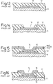
- an insulation layer 12 is first formed on an underlying patterned wiring line 10 made up of copper or the like by the application or lamination of a material therefor (Fig. 13).
- a via hole 14 is then formed in the insulation layer 12 by laser machining or photolithography (Fig. 14).
- a copper plated layer 16 is subsequently formed so as to cover the inside of the via hole 14, where part of the patterned wiring line 10 is exposed at the bottom, and the top surface of the insulation layer 12, the copper plated layer 16 consisting of an electrolessly plated copper film 16a and an electroplated copper film 16b which are sequentially formed (Fig. 15).
- the copper plated layer 16 is then etched to provide an overlaying patterned wiring line 18 (Fig. 16).
- the change in level on the surface of the formed insulation layer which results from the underlying wiring line 10 having a top level higher than the surface of a substrate 8 on which the wiring line 10 is formed, can be cancelled by filling the inside of the via hole 14 with a conductor paste or insulating resin.
- a planarization process increases the number of steps involved, and has a limited effect.
- the inside of a via hole is designed to be filled with copper plating by, for example, contriving the agitation of a plating solution to thereby satisfactorily penetrate the inside of the via hole, or adding a plating promoting agent to thereby improve the throwing power of plating in the via hole.
- An object of the invention is to provide a method of plating for filling via holes in which even via holes having a small diameter and a large aspect ratio can be satisfactorily filled with copper plating.
- the method of plating for filling via holes of the invention in which each via hole formed in an insulation layer covering a substrate so as to expose, at its bottom, part of a conductor layer located on the substrate, is plated with copper to be filled with the plated metal, is characterized by comprising the steps of forming a copper film on the top surface of the insulation layer covering the substrate, and the side walls and bottoms of the respective via holes, immersing the substrate having the copper film formed in an aqueous solution containing a plating promoter to thereby deposit the plating promoter on the surface of the copper film, removing the plating promoter from the surface of the copper film located on the insulation layer and leaving the plating promoter on the side walls and bottoms of the respective via holes, and subsequently electroplating the substrate having the copper film formed with copper to thereby fill the via holes with the plated copper and simultaneously form a continuous copper film which eventually covers the via holes filled with the plated copper as well as the copper film previously formed on the insulation layer.
- the plating promoter can be securely deposited within the via holes, and plating conditions in the via holes can be different from those on the top surface of the insulation layer. Also, a current for plating can be concentrated within the via holes, and even via holes having a large aspect ratio can be satisfactorily plated with copper.
- the alkyl group denoted by R has one to six carbon atoms.
- n is selected from the integers of one to six, and m is also selected from the integers of one to six.
- the sulfur compound may be used in an aqueous solution containing a non-ionic surfactant for improving wettability of the solution, such as a polyethylene glycol or polypropylene glycol.
- Examples of the plating promoters represented by formula (I) include sodium 3-mercapto-1-propanesulfonate and sodium 2-mercaptoethanesulfonate, and examples of the plating promoters represented by formula (II) includes disodium bis-(3-sulfopropyl)-disulfide.
- the step of removal of the plating promoter from the surface of the copper film located on the insulation layer can be carried out by, for example, an etching process using an etching solution for copper, a cyanide electrolytic treatment using a cyanide electrolytic bath, a ultraviolet radiation treatment obliquely irradiating the surface of the copper film on the insulation layer with ultraviolet radiation, or a treatment of polishing the surface of the copper film on the top of the insulation layer.
- the step of removal of the plating promoter on the surface of the copper film located on the insulation layer is omitted and, after the step of immersion of the substrate in a plating promoter-containing solution, a reverse electrolytic treatment is performed at an early stage of the step of electroplating with copper.
- the step of removal of the plating promoter on the surface of the copper film located on the insulation layer is omitted and, after the step of immersion of the substrate in a plating promoter-containing solution, a pulse plating in which the direction of current applied is periodically reversed is used in the step of electroplating with copper.
- an electroplating solution free of a plating promoter is used.
- an electroplating solution free of a plating promoter may be used in the step of electroplating with copper, carrying out the step of immersion of the substrate using, as the plating promoter, sodium 3-mercapto-1-propanesulfonate or sodium 2-mercaptoethanesulfonate, and omitting the step of removal of the plating promoter on the surface of the insulation layer.
- a strike plating of copper is provided on the surface of the copper film.
- an insulation layer 12 is formed on a surface of a substrate on which patterned wiring lines 10 are provided, by applying or laminating an insulation material thereon, and it is then processed, by laser machining or photolithography, to provide via holes 14 which expose, at their bottom, part of the underlying wiring line.
- an insulation layer is formed by heating and pressing a sheet of polyphenyleneether (PPE) for lamination and is machined by a YAG laser or carbon dioxide laser to form via holes.
- PPE polyphenyleneether
- a plated copper film 21 is formed so as to cover the top surface of the insulation layer 12 and the side wall and bottom of the via hole 14 by electroless plating.
- the plated copper film 21 may be formed by sputtering or evaporation in lieu of electroless plating.
- the substrate 20 thus processed is then immersed in an aqueous solution containing a plating promoter, to thereby deposit the plating promoter and form a layer of plating promoter 22 on the plated copper film 21, as shown in Fig. 2.
- the formed layer of plating promoter is very thin, and is schematically represented by the broken line in Fig. 2 as well as the drawings subsequently referred to.
- a sulfur compound can be used, the sulfur compound being represented by the general formula: wherein X denotes sodium, potassium, or hydrogen, R denotes hydrogen or an alkyl group, and n is an integer of one or larger, such as sodium 3-mercapto-1-propanesulfonate or sodium 2-mercaptoethanesulfonate, or the general formula: wherein X denotes sodium, potassium, or hydrogen, R denotes hydrogen or an alkyl group, n is an integer of one or larger, and m is an integer of one or larger, such as disodium bis-(3-sulfopropyl) disulfide.
- the alkyl group denoted by R has one to six carbon atoms, such as methyl, ethyl, propyl, butyl, pentyl, and hexyl. It is also preferred that n is selected from the integers of one to six, and m is selected from the integers of one to six. If n and m are larger than six, the compound is oily and is expected to be indissoluble in an aqueous solution.
- Such a plating promoter is one of additives which are added to a solution for copper plating, and is also known as a brightening agent or brightener. It is believed that when a plating promoter is deposited on the surface of an object to be plated, the resistance involved with plating is lowered, and a current for plating is concentrated so that plating is promoted.
- the plating promoter in the invention is defined to be a sulfur compound which shifts a potential of a cathode relative to a potential of a reference electrode placed in a solution for copper plating toward the positive side when it is added to the copper plating solution as compared to the case of no addition thereof.
- a single plating promoter may be used, or a mixture of two or more plating promoters may be also used.
- An aqueous solution may contain the plating promoter in a concentration of several ppm to several percent, although the concentration of plating promoter is not limited to this range.
- the aqueous solution may contain an acidic ingredient, such as sulfuric acid or copper sulfate, for the inhibition of the generation of fungi.
- the solution of plating promoter is used at a normal temperature. It is preferred that the substrate 20 having the plated copper film 21 is immersed in the solution of plating promoter for a relatively long time of the order of approximately 5 to 15 minutes so that the solution can satisfactorily penetrate into the via holes 14, although the time of immersion of the substrate 20 depends on the concentration of the solution of the plating promoter. It is also preferred that the solution of plating promoter is stirred, or the substrate 20 is rocked in the solution, for the acceleration of the penetration of solution. For the improvement of the wettability of the substrate 20 by a solution of plating promoter, it is preferred that the substrate 20 is previously immersed in a pretreatment solution, such as a solution of a surfactant or the like. After the immersion, the substrate 20 is washed by water in an appropriate manner. The plating promoter deposited to the substrate is not removed even after water washing.
- the deposited plating promoter is then removed from the surface of the copper film 21 located on the insulation layer 12, and is left on the side wall and bottom of the via hole 14.
- the removal of the plating promoter can be achieved by immersing the substrate 20 in a solution for etching copper, such as an aqueous solution of ferrous chloride. It is preferred that after the immersion of the substrate 20 in this etching solution, the substrate is immediately water-washed.
- the etching solution will not penetrate into the via holes 14 and, accordingly, the plating promoter on the surface of the copper film 21 located on the insulation layer 12, and except for the plating promoter inside the via hole 14, can be selectively removed.
- the step of removal of the plating promoter can be also carried out by a cyanide electrolytic treatment using a cyanide electrolytic bath.
- the plating promoter may be removed by the decomposition thereof by a ultraviolet radiation treatment obliquely irradiating the surface of the copper film 21 on the insulation layer 12 with ultraviolet radiation.
- the oblique irradiation will not fully go into the via holes 14 and, accordingly, the plating promoter deposited on a portion other than the areas where the via holes are located of the copper film 21 can be selectively removed.
- the plating promoter on the surface of the copper film 21 located on the insulation layer 12 can also be selectively removed by a treatment of polishing that surface of the copper film 21 on the insulation layer 12.
- the substrate 20 is subjected to an electroplating process so as to deposit copper on the surface of the insulation layer 12, which has been exposed in the step of selective removal of the plating promoter thereon, and on the layer of plating promoter 22 left in the via holes 14, to thereby fill the via holes 14 with plated copper.
- the substrate 20 has a continuous layer of copper 23 which completely covers the surface thereof provided with the wiring lines 10, insulation layer 12, and the via holes 14.
- additives examples are as follows: PEG4000 (polyethylene glycol) 180 g/L PPG425 (polypropylene glycol) 72 g/L
- such a polymer component is used as an additive because its capability of improving the wettability of the plating solution.
- the above solution for copper plating does not contain a plating promoter. It is preferred that the plating solution is free of a plating promoter for the stability of the plating solution and in the case of the omission of the step of removal of the plating promoter described above, although it may contain a plating promoter in such a case where electroplating the copper film 21 with copper to make the layer 23 as illustrated in Fig. 4 is achieved using periodic pulse reverse (PPR) of plating current.
- PPR periodic pulse reverse
- composition of the copper plating solution is not limited to the example referred to above.
- a current 26 for plating is concentrated in the via hole 14 in which the layer of plating promoter 22 is retained, as illustrated in Fig. 6, and the via hole 14 can be completely filled with the electroplated copper 23, as shown in Fig. 4.
- the layer of electroplated copper 23 and the underlying copper film 21 are then patterned by etching, to thereby form upper wiring lines 24, as shown in Fig. 5.
- Fig. 12 Characteristics of different plating promoters are shown in Fig. 12.
- the curves indicated in Fig. 12 were obtained by detecting a potential of a cathode relative to a potential of a reference electrode placed in the plating solution described above while electroplating a substrate with copper using the plating solution, which contained no plating promoter, for 5 minutes, and subsequently using the plating solution to which a plating promoter was added in a concentration of 1 part per million (ppm).
- ppm part per million
- sodium 3-mercapto-1-propanesulfonate, sodium 2-mercaptoethanesulfonate, and disodium bis-(3-sulfopropyl) disulfide were used.
- the cathode potential after the addition of the plating promoter was shifted toward the positive side as compared to the solution before the addition thereof, which means that the solution containing the plating promoter makes it easy to deposit copper on a substrate at a lower voltage than that required in the case of a plating solution containing no plating promoter.
- a solution for electroplating with copper containing a plating promoter may be used. Even in this case, since the plating promoter is already deposited in the vial holes 14 in the previous step as described above, the current can be concentrated in the via hole 14, and the via holes can be filled with the plated copper.
- a reverse electrolytic treatment may be performed at an early stage of the step of electroplating with copper. For example, a few minutes after the initiation of the electroplating with copper, copper-plating is carried out for a few minutes while reversing the polarities of electrodes (anode and cathode) at, for instance, 30 second intervals. On the reversal of the polarities of the electrodes, the removal of the plating promoter deposited on portion outside the via holes 14 is accelerated and, accordingly, the current for plating can be concentrated in the via holes 14, to thereby completely fill the via holes 14 with the plated copper.
- electrodes anode and cathode
- a pulse plating in which the direction of current applied is periodically reversed is used in the step of electroplating with copper.
- PPR electroplating pulse plating in which a current (plating current) is applied in the normal direction for 10 microseconds and a current in the reverse direction is applied for 1 microsecond, the plating promoter deposited on portion outside the via holes 14 is removed and, accordingly, the via holes 14 can be completely filled with the plated copper.
- the via holes 14 can also be filled with plated copper only by the use of a solution for copper plating free of a plating promoter in the step of electroplating with copper, with the step of selective removal of the plating promoter deposited on the copper film 21 located on the insulation layer 12 being omitted. Also in this case, since the plating promoter is already deposited in the vial holes 14 in the previous step as described above, the current for plating can be concentrated in the via hole 14 so as to completely fill the via holes with the plated copper.
- an additional plating step which forms, by electroplating, a strike plating film of copper on the film 21 of electrolessly plated copper, is interposed between the step of electroless plating and the step of immersion of the substrate in the solution containing the plating promoter. Since a film of pure copper is formed on the film 21 of electrolessly plated copper by this additional step, failure of the deposition of the plating promoter due to, for instance, the oxidation of the surface of the film 21 of electrolessly plated copper can be prevented, and the plating promoter can be deposited evenly and uniformly on the clean surface of copper so as to completely fill the via holes 14 with the subsequently plated copper.
- the surface of a silicon substrate provided with an insulation layer having via holes formed so as to expose, at their bottoms, part of the underlying conductor layer was electroless-plated with copper.
- the substrate was then immersed in an aqueous solution of 1% sodium 3-mercapto-1-propanesulfonate (plating promoter) for 15 minutes with rocking, to thereby deposit the plating promoter on the film of the electroless-plated copper.
- plating promoter sodium 3-mercapto-1-propanesulfonate
- the substrate was placed in a cyanide electrolytic bath (20 g/L NaCN and 140 g/L NaOH), and was electrolytically treated at a normal temperature and at an applied voltage of 1.4 volts for 30 seconds, with the substrate being used as a cathode, to thereby remove the plating promoter on the film of the electroless-plated copper located on the insulation layer and leave the plating promoter within the via holes.
- a cyanide electrolytic bath (20 g/L NaCN and 140 g/L NaOH)
- the substrate was electroplated with copper using a plating bath containing the following ingredients: copper sulfate 120 g/L sulfuric acid 190 g/L chloride ion 50 ppm PEG4000 (180 g/L solution) 40 mL/L at a normal temperature and a current density of 1 A/dm 2 for 100 minutes.
- a plating bath containing the following ingredients: copper sulfate 120 g/L sulfuric acid 190 g/L chloride ion 50 ppm PEG4000 (180 g/L solution) 40 mL/L at a normal temperature and a current density of 1 A/dm 2 for 100 minutes.
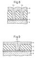
- the via holes were completely filled with the plated copper, as shown in Figs.
- FIG. 7 and 8 which respectively illustrate a via hole 14a having a diameter at its opening of 46 micrometers, a depth of 53 micrometers, and an aspect ratio of 1.15, and a via hole 14b having a diameter at its opening of 28 micrometers, a depth of 53 micrometers, and an aspect ratio of 1.89.
- the surface of a silicon substrate provided with an insulation layer having via holes formed so as to expose, at their bottoms, part of the underlying conductor layer was electroless-plated with copper.
- the substrate was then immersed in an aqueous solution containing 1.5 g/L of sodium 3-mercapto-1-propanesulfonate (plating promoter) for 3 minutes, to thereby deposit the plating promoter on the film of the electroless-plated copper.
- the substrate was electroplated with copper using the plating bath used in Example 1 at a normal temperature and a current density of 1 A/dm 2 for 100 minutes.
- the polarities of electrodes were reversed at 30 second interval from 2 minutes to 9 minutes after the initiation of the plating.
- Figs. 9 and 10 respectively illustrate a via hole 14c having a diameter at its opening of 40 micrometers and an aspect ratio of about 0.5, and a via hole 14d having a diameter at its opening of 60 micrometers and an aspect ratio of about 0.5.
- the surface of a silicon substrate provided with an insulation layer having via holes formed so as to expose, at their bottoms, part of the underlying conductor layer was electroless-plated with copper.
- the substrate was then immersed in an aqueous solution of 1% sodium 3-mercapto-1-propanesulfonate (plating promoter) for 10 minutes with rocking, to thereby deposit the plating promoter on the film of the electroless-plated copper.
- plating promoter sodium 3-mercapto-1-propanesulfonate
- the substrate was PPR-electroless-plated with copper using the plating bath used in Example 1 at the following conditions: time of current applied in normal direction 10 ms time of current applied in reverse direction 0.5 ms current density in normal direction 1 A/dm 2 current density in reverse direction 3 A/dm 2 time of plating 100 minutes
- the via holes 14e having a diameter at its opening of 100 micrometers and a depth of 30 micrometers could be completely filled with the plated copper, as shown in Fig. 11.
Landscapes
- Chemical & Material Sciences (AREA)
- Engineering & Computer Science (AREA)
- Organic Chemistry (AREA)
- Electrochemistry (AREA)
- Materials Engineering (AREA)
- Metallurgy (AREA)
- Chemical Kinetics & Catalysis (AREA)
- Manufacturing & Machinery (AREA)
- Microelectronics & Electronic Packaging (AREA)
- Printing Elements For Providing Electric Connections Between Printed Circuits (AREA)
- Electroplating Methods And Accessories (AREA)
- Manufacturing Of Printed Wiring (AREA)
- Production Of Multi-Layered Print Wiring Board (AREA)
Abstract

Description


| copper sulfate | 120 g/L |
| sulfuric acid | 190 g/L |
| chloride ion | 50 ppm |
| additive | 40 mL/L |
| PEG4000 (polyethylene glycol) | 180 g/L |
| PPG425 (polypropylene glycol) | 72 g/L |
| copper sulfate | 120 g/L |
| sulfuric acid | 190 g/L |
| chloride ion | 50 ppm |
| PEG4000 (180 g/L solution) | 40 mL/L |
| time of current applied in | 10 ms |
| time of current applied in reverse direction | 0.5 ms |
| current density in normal direction | 1 A/dm2 |
| current density in reverse direction | 3 A/dm2 |
| time of plating | 100 minutes |
Claims (11)
- A method of plating for filling via holes, in which each of via holes formed in an insulation layer covering a substrate so as to expose, at its bottom, part of a conductor layer located on the substrate, is plated with copper to be filled with the plated metal, the method comprising the steps of:forming a copper film on the top surface of the insulation layer covering the substrate, and the side walls and bottoms of the respective via holes,immersing the substrate having the copper film formed in an aqueous solution containing a plating promoter to thereby deposit the plating promoter on the surface of the copper film,removing the plating promoter from the surface of the copper film located on the insulation layer and leaving the plating promoter on the side walls and bottoms of the respective via holes, andelectroplating the substrate having the copper film formed with copper to thereby fill the via holes with the plated copper and simultaneously form a continuous copper film which eventually covers the via holes filled with the plated copper as well as the copper film previously formed on the insulation layer.
- The method of claim 2, wherein, as the plating promoter, a sulfur compound or a mixtures of sulfur compounds is used, the sulfur compound being selected from the group consisting of the compounds represented by the general formulae:and
 wherein X denotes sodium, potassium, or hydrogen, R denotes hydrogen or an alkyl group, n is an integer of one or larger, and m is an integer of one or larger.
- The method of claim 2, wherein the sulfur compound is selected from the group consisting of sodium 3-mercapto-1-propanesulfonate, sodium 2-mercaptoethanesulfonate, and disodium bis-(3-sulfopropyl)-disulfide.
- The method of any preceding claim, wherein the aqueous solution containing the plating promoter further comprises a non-ionic surfactant.
- The method of claim 4, wherein the non-ionic surfactant is a polyethylene glycol or polypropylene glycol.
- The method of any preceding claim, wherein the plating promoter is removed by a process or treatment selected from the group of (1) an etching process using an etching solution for copper, (2) a cyanide electrolytic treatment using a cyanide electrolytic bath, (3) a ultraviolet radiation treatment obliquely irradiating the surface of the copper film on the insulation layer with ultraviolet radiation, and (4) a treatment of polishing the surface of the copper film on the top of the insulation layer.
- The method of any preceding claim, wherein the step of removal of the plating promoter is omitted and, after the step of immersion of the substrate in the plating promoter-containing solution, a reverse electrolytic treatment is performed at an early stage of the step of electroplating with copper.
- The method of any preceding claim, wherein the step of removal of the plating promoter is omitted and, after the step of immersion of the substrate in the plating promoter-containing solution, a pulse plating in which the direction of current applied is periodically reversed is used in the step of electroplating with copper.
- The method of any one of claims 1 to 7, wherein the step of electroplating with copper is carried out by the use of an electroplating solution free of a plating promoter.
- The method of claim 1, wherein the step of immersion of the substrate in the plating promoter-containing solution is carried out using, as the plating promoter, sodium 3-mercapto-1-propanesulfonate or sodium 2-mercaptoethanesulfonate, the step of removal of the plating promoter is omitted, and the step of electroplating with copper is carried out using an electroplating solution free of a plating promoter.
- The method of any preceding claim, wherein, prior to the step of immersion of the substrate in the plating promoter-containing solution, a strike plating of copper is provided on the surface of the copper film.
Applications Claiming Priority (4)
| Application Number | Priority Date | Filing Date | Title |
|---|---|---|---|
| JP2000023794 | 2000-02-01 | ||
| JP2000023794 | 2000-02-01 | ||
| JP2000334044A JP3594894B2 (en) | 2000-02-01 | 2000-11-01 | Via filling plating method |
| JP2000334044 | 2000-11-01 |
Publications (3)
| Publication Number | Publication Date |
|---|---|
| EP1122989A2 true EP1122989A2 (en) | 2001-08-08 |
| EP1122989A3 EP1122989A3 (en) | 2002-07-03 |
| EP1122989B1 EP1122989B1 (en) | 2007-02-28 |
Family
ID=26584623
Family Applications (1)
| Application Number | Title | Priority Date | Filing Date |
|---|---|---|---|
| EP01300837A Expired - Lifetime EP1122989B1 (en) | 2000-02-01 | 2001-01-31 | Method of plating for filling via holes |
Country Status (6)
| Country | Link |
|---|---|
| US (1) | US6755957B2 (en) |
| EP (1) | EP1122989B1 (en) |
| JP (1) | JP3594894B2 (en) |
| KR (1) | KR100730326B1 (en) |
| DE (1) | DE60126853T2 (en) |
| TW (1) | TW574438B (en) |
Cited By (14)
| Publication number | Priority date | Publication date | Assignee | Title |
|---|---|---|---|---|
| WO2002015245A3 (en) * | 2000-08-10 | 2002-07-04 | Nutool Inc | Plating method and apparatus that creates a differential between additive disposed on a top surface and a cavity surface of a workpiece using an external influence |
| WO2001083854A3 (en) * | 2000-04-27 | 2002-10-03 | Intel Corp | Electroplating bath composition and method of using |
| US6534116B2 (en) | 2000-08-10 | 2003-03-18 | Nutool, Inc. | Plating method and apparatus that creates a differential between additive disposed on a top surface and a cavity surface of a workpiece using an external influence |
| US6858121B2 (en) | 2000-08-10 | 2005-02-22 | Nutool, Inc. | Method and apparatus for filling low aspect ratio cavities with conductive material at high rate |
| US7214305B2 (en) | 2003-05-14 | 2007-05-08 | Kabushiki Kaisha Toshiba | Method of manufacturing electronic device |
| EP1249861A3 (en) * | 2001-03-23 | 2007-11-21 | Interuniversitair Micro-Elektronica Centrum | A multi-step method for metal deposition |
| EP1324384A3 (en) * | 2001-12-20 | 2007-12-26 | Shipley Co. L.L.C. | Via filling method |
| US7550070B2 (en) | 2006-02-03 | 2009-06-23 | Novellus Systems, Inc. | Electrode and pad assembly for processing conductive layers |
| US7732329B2 (en) | 2006-08-30 | 2010-06-08 | Ipgrip, Llc | Method and apparatus for workpiece surface modification for selective material deposition |
| DE10321509B4 (en) * | 2002-05-17 | 2012-06-06 | Denso Corporation | A method of filling blind vias and forming an electrode |
| EP2778261A1 (en) * | 2013-03-14 | 2014-09-17 | Rohm and Haas Electronic Materials LLC | Method of filling through-holes |
| CN107087353A (en) * | 2016-02-15 | 2017-08-22 | 罗门哈斯电子材料有限责任公司 | Fill method of the through hole to reduce space and other defects |
| EP3826439A1 (en) * | 2019-11-19 | 2021-05-26 | AT & S Austria Technologie & Systemtechnik Aktiengesellschaft | Laminated component carrier with blind hole having wedges filled with filling medium by sputtering and back-sputtering |
| CN113747664A (en) * | 2020-05-29 | 2021-12-03 | 深南电路股份有限公司 | Printed circuit board and manufacturing method thereof |
Families Citing this family (39)
| Publication number | Priority date | Publication date | Assignee | Title |
|---|---|---|---|---|
| US7449098B1 (en) | 1999-10-05 | 2008-11-11 | Novellus Systems, Inc. | Method for planar electroplating |
| US7531079B1 (en) | 1998-10-26 | 2009-05-12 | Novellus Systems, Inc. | Method and apparatus for uniform electropolishing of damascene IC structures by selective agitation |
| US6921551B2 (en) | 2000-08-10 | 2005-07-26 | Asm Nutool, Inc. | Plating method and apparatus for controlling deposition on predetermined portions of a workpiece |
| JP4000796B2 (en) * | 2001-08-08 | 2007-10-31 | 株式会社豊田自動織機 | Via hole copper plating method |
| US20040011654A1 (en) * | 2001-10-16 | 2004-01-22 | Kenji Nakamura | Method of copper plating small diameter hole |
| JP2003168860A (en) * | 2001-11-30 | 2003-06-13 | Cmk Corp | Printed wiring board and method of manufacturing the same |
| US7405163B1 (en) * | 2003-12-17 | 2008-07-29 | Novellus Systems, Inc. | Selectively accelerated plating of metal features |
| US7449099B1 (en) * | 2004-04-13 | 2008-11-11 | Novellus Systems, Inc. | Selectively accelerated plating of metal features |
| US7799200B1 (en) | 2002-07-29 | 2010-09-21 | Novellus Systems, Inc. | Selective electrochemical accelerator removal |
| US8530359B2 (en) | 2003-10-20 | 2013-09-10 | Novellus Systems, Inc. | Modulated metal removal using localized wet etching |
| US8158532B2 (en) | 2003-10-20 | 2012-04-17 | Novellus Systems, Inc. | Topography reduction and control by selective accelerator removal |
| DE102004005300A1 (en) * | 2004-01-29 | 2005-09-08 | Atotech Deutschland Gmbh | Process for treating carrier material for the production of powder carriers and application of the process |
| US20050224358A1 (en) * | 2004-03-30 | 2005-10-13 | Lsi Logic Corporation | Method for improved local planarity control during electropolishing |
| JP4150930B2 (en) * | 2004-10-21 | 2008-09-17 | 日立電線株式会社 | Method for manufacturing double-sided wiring tape carrier for semiconductor device |
| WO2006129354A1 (en) * | 2005-06-01 | 2006-12-07 | Matsushita Electric Industrial Co., Ltd. | Circuit board, method for manufacturing such circuit board, and electronic component using such circuit board |
| JP4759416B2 (en) * | 2006-03-20 | 2011-08-31 | 新光電気工業株式会社 | Non-cyanide electroless gold plating solution and electroless gold plating method |
| US7405154B2 (en) * | 2006-03-24 | 2008-07-29 | International Business Machines Corporation | Structure and method of forming electrodeposited contacts |
| US7575666B2 (en) * | 2006-04-05 | 2009-08-18 | James Watkowski | Process for electrolytically plating copper |
| JP4862508B2 (en) * | 2006-06-12 | 2012-01-25 | 日立電線株式会社 | Conductor pattern forming method |
| US8500985B2 (en) | 2006-07-21 | 2013-08-06 | Novellus Systems, Inc. | Photoresist-free metal deposition |
| US20080148561A1 (en) * | 2006-12-22 | 2008-06-26 | Motorola, Inc. | Methods for making printed wiring boards |
| KR100832705B1 (en) * | 2006-12-23 | 2008-05-28 | 동부일렉트로닉스 주식회사 | Via plating method of system-in-package and its system |
| KR200454218Y1 (en) * | 2008-10-08 | 2011-06-23 | 주식회사강산 | Handrail |
| AT506583B9 (en) | 2008-10-23 | 2009-12-15 | Happy Plating Gmbh | ELECTROCHEMICAL COATING PROCESS |
| US8168540B1 (en) | 2009-12-29 | 2012-05-01 | Novellus Systems, Inc. | Methods and apparatus for depositing copper on tungsten |
| KR101705734B1 (en) | 2011-02-18 | 2017-02-14 | 삼성전자주식회사 | Copper electroplating solution and method of copper electroplating using the same |
| EP2551375A1 (en) * | 2011-07-26 | 2013-01-30 | Atotech Deutschland GmbH | Electroless nickel plating bath composition |
| US9598787B2 (en) * | 2013-03-14 | 2017-03-21 | Rohm And Haas Electronic Materials Llc | Method of filling through-holes |
| JP6350064B2 (en) * | 2013-10-09 | 2018-07-04 | 日立化成株式会社 | Manufacturing method of multilayer wiring board |
| JP6327463B2 (en) * | 2013-10-09 | 2018-05-23 | 日立化成株式会社 | Manufacturing method of multilayer wiring board |
| JP6350063B2 (en) * | 2013-10-09 | 2018-07-04 | 日立化成株式会社 | Multilayer wiring board |
| US10154598B2 (en) * | 2014-10-13 | 2018-12-11 | Rohm And Haas Electronic Materials Llc | Filling through-holes |
| JP6625872B2 (en) | 2015-11-25 | 2019-12-25 | 新光電気工業株式会社 | Wiring board and method of manufacturing wiring board |
| US10508357B2 (en) | 2016-02-15 | 2019-12-17 | Rohm And Haas Electronic Materials Llc | Method of filling through-holes to reduce voids and other defects |
| JP2017162895A (en) * | 2016-03-08 | 2017-09-14 | 株式会社ジェイデバイス | Wiring structure, printed circuit board, semiconductor device, and manufacturing method of wiring structure |
| KR102254649B1 (en) | 2020-04-14 | 2021-05-24 | 주식회사 디에이피 | Method for electric copper plating of PCB |
| CN113795086B (en) * | 2021-10-19 | 2023-04-14 | 重庆新固兴科技有限公司 | Double-sided false sticker machine |
| CN115003032B (en) * | 2022-06-21 | 2023-03-07 | 东莞市国盈电子有限公司 | A motor drive control circuit board and its manufacturing process |
| CN117265530A (en) * | 2023-09-06 | 2023-12-22 | 九江德福科技股份有限公司 | A method to eliminate light transmission points of composite copper foil |
Family Cites Families (11)
| Publication number | Priority date | Publication date | Assignee | Title |
|---|---|---|---|---|
| DE1075398B (en) * | 1954-03-22 | 1960-02-11 | DEHYDAG Deutsche Hydrierwerke G.m.b.H., Düsseldorf | Bath for the galvanic production of metal coatings |
| JPH01143797A (en) * | 1987-11-30 | 1989-06-06 | Mitsumi Electric Co Ltd | Press device |
| US5174886A (en) | 1991-02-22 | 1992-12-29 | Mcgean-Rohco, Inc. | High-throw acid copper plating using inert electrolyte |
| US5252196A (en) | 1991-12-05 | 1993-10-12 | Shipley Company Inc. | Copper electroplating solutions and processes |
| JPH1143797A (en) * | 1997-07-25 | 1999-02-16 | Hideo Honma | Via filling method |
| JPH11298141A (en) * | 1998-04-08 | 1999-10-29 | Hitachi Ltd | Electronic device manufacturing method |
| KR100336829B1 (en) | 1998-04-10 | 2002-05-16 | 모기 쥰이찌 | Fabricating method of multilayered wiring substrate |
| KR100654413B1 (en) | 1998-04-30 | 2006-12-05 | 가부시키가이샤 에바라 세이사꾸쇼 | Substrate Plating Method |
| US6534116B2 (en) * | 2000-08-10 | 2003-03-18 | Nutool, Inc. | Plating method and apparatus that creates a differential between additive disposed on a top surface and a cavity surface of a workpiece using an external influence |
| JP3124523B2 (en) | 1999-01-28 | 2001-01-15 | 日本エレクトロプレイテイング・エンジニヤース株式会社 | Copper plating method |
| US6224737B1 (en) * | 1999-08-19 | 2001-05-01 | Taiwan Semiconductor Manufacturing Company | Method for improvement of gap filling capability of electrochemical deposition of copper |
-
2000
- 2000-11-01 JP JP2000334044A patent/JP3594894B2/en not_active Expired - Fee Related
-
2001
- 2001-01-30 US US09/772,457 patent/US6755957B2/en not_active Expired - Lifetime
- 2001-01-31 KR KR20010004601A patent/KR100730326B1/en not_active Expired - Lifetime
- 2001-01-31 EP EP01300837A patent/EP1122989B1/en not_active Expired - Lifetime
- 2001-01-31 DE DE60126853T patent/DE60126853T2/en not_active Expired - Lifetime
- 2001-01-31 TW TW90101961A patent/TW574438B/en not_active IP Right Cessation
Cited By (19)
| Publication number | Priority date | Publication date | Assignee | Title |
|---|---|---|---|---|
| WO2001083854A3 (en) * | 2000-04-27 | 2002-10-03 | Intel Corp | Electroplating bath composition and method of using |
| US6893550B2 (en) | 2000-04-27 | 2005-05-17 | Intel Corporation | Electroplating bath composition and method of using |
| US6534116B2 (en) | 2000-08-10 | 2003-03-18 | Nutool, Inc. | Plating method and apparatus that creates a differential between additive disposed on a top surface and a cavity surface of a workpiece using an external influence |
| US6858121B2 (en) | 2000-08-10 | 2005-02-22 | Nutool, Inc. | Method and apparatus for filling low aspect ratio cavities with conductive material at high rate |
| US7404886B2 (en) | 2000-08-10 | 2008-07-29 | Novellus Systems, Inc. | Plating by creating a differential between additives disposed on a surface portion and a cavity portion of a workpiece |
| WO2002015245A3 (en) * | 2000-08-10 | 2002-07-04 | Nutool Inc | Plating method and apparatus that creates a differential between additive disposed on a top surface and a cavity surface of a workpiece using an external influence |
| EP1249861A3 (en) * | 2001-03-23 | 2007-11-21 | Interuniversitair Micro-Elektronica Centrum | A multi-step method for metal deposition |
| EP1324384A3 (en) * | 2001-12-20 | 2007-12-26 | Shipley Co. L.L.C. | Via filling method |
| DE10321509B4 (en) * | 2002-05-17 | 2012-06-06 | Denso Corporation | A method of filling blind vias and forming an electrode |
| CN1327479C (en) * | 2003-05-14 | 2007-07-18 | 株式会社东芝 | Method of manufacturing electronic device |
| US7214305B2 (en) | 2003-05-14 | 2007-05-08 | Kabushiki Kaisha Toshiba | Method of manufacturing electronic device |
| US7550070B2 (en) | 2006-02-03 | 2009-06-23 | Novellus Systems, Inc. | Electrode and pad assembly for processing conductive layers |
| US7732329B2 (en) | 2006-08-30 | 2010-06-08 | Ipgrip, Llc | Method and apparatus for workpiece surface modification for selective material deposition |
| US8012875B2 (en) | 2006-08-30 | 2011-09-06 | Ipgrip, Llc | Method and apparatus for workpiece surface modification for selective material deposition |
| EP2778261A1 (en) * | 2013-03-14 | 2014-09-17 | Rohm and Haas Electronic Materials LLC | Method of filling through-holes |
| CN107087353A (en) * | 2016-02-15 | 2017-08-22 | 罗门哈斯电子材料有限责任公司 | Fill method of the through hole to reduce space and other defects |
| EP3826439A1 (en) * | 2019-11-19 | 2021-05-26 | AT & S Austria Technologie & Systemtechnik Aktiengesellschaft | Laminated component carrier with blind hole having wedges filled with filling medium by sputtering and back-sputtering |
| CN113747664A (en) * | 2020-05-29 | 2021-12-03 | 深南电路股份有限公司 | Printed circuit board and manufacturing method thereof |
| CN113747664B (en) * | 2020-05-29 | 2024-01-05 | 深南电路股份有限公司 | Printed circuit board and manufacturing method thereof |
Also Published As
| Publication number | Publication date |
|---|---|
| JP2001291954A (en) | 2001-10-19 |
| DE60126853T2 (en) | 2007-08-30 |
| EP1122989B1 (en) | 2007-02-28 |
| DE60126853D1 (en) | 2007-04-12 |
| US6755957B2 (en) | 2004-06-29 |
| JP3594894B2 (en) | 2004-12-02 |
| KR100730326B1 (en) | 2007-06-19 |
| EP1122989A3 (en) | 2002-07-03 |
| TW574438B (en) | 2004-02-01 |
| KR20010078217A (en) | 2001-08-20 |
| US20010013472A1 (en) | 2001-08-16 |
Similar Documents
| Publication | Publication Date | Title |
|---|---|---|
| EP1122989B1 (en) | Method of plating for filling via holes | |
| US7135404B2 (en) | Method for applying metal features onto barrier layers using electrochemical deposition | |
| US6863793B2 (en) | Sequential electrodeposition of metals using modulated electric fields for manufacture of circuit boards having features of different sizes | |
| EP2010698B1 (en) | Process for electrolytically plating copper | |
| US6210555B1 (en) | Electrodeposition of metals in small recesses for manufacture of high density interconnects using reverse pulse plating | |
| US6303014B1 (en) | Electrodeposition of metals in small recesses using modulated electric fields | |
| US6652727B2 (en) | Sequential electrodeposition of metals using modulated electric fields for manufacture of circuit boards having features of different sizes | |
| KR100877923B1 (en) | Electrolytic Copper Plating | |
| US6524461B2 (en) | Electrodeposition of metals in small recesses using modulated electric fields | |
| US6750144B2 (en) | Method for electrochemical metallization and planarization of semiconductor substrates having features of different sizes | |
| JP5078142B2 (en) | Electrical treatment for filling metal in through holes, especially electrical treatment for filling copper in printed circuit board through holes | |
| EP2796019A1 (en) | Method for combined through-hole plating and via filling | |
| US20030221967A1 (en) | Via filling method | |
| KR100596992B1 (en) | Method for depositing lead-free tin alloy | |
| TWI883333B (en) | A method of plating a metal on an electronic substrate, an apparatus for electroplating a metal on an electronic subtrate, an electronic substrate and a printed circuit board | |
| KR20030053008A (en) | Via filling method | |
| US20040222104A1 (en) | Electroplating composition | |
| KR102835665B1 (en) | Method of filling through-holes to reduce voids | |
| JPS6257120B2 (en) | ||
| US20050092616A1 (en) | Baths, methods, and tools for superconformal deposition of conductive materials other than copper | |
| JP2000234198A (en) | Electrodeposition method inside the aperture |
Legal Events
| Date | Code | Title | Description |
|---|---|---|---|
| PUAI | Public reference made under article 153(3) epc to a published international application that has entered the european phase |
Free format text: ORIGINAL CODE: 0009012 |
|
| AK | Designated contracting states |
Kind code of ref document: A2 Designated state(s): AT BE CH CY DE DK ES FI FR GB GR IE IT LI LU MC NL PT SE TR |
|
| AX | Request for extension of the european patent |
Free format text: AL;LT;LV;MK;RO;SI |
|
| PUAL | Search report despatched |
Free format text: ORIGINAL CODE: 0009013 |
|
| AK | Designated contracting states |
Kind code of ref document: A3 Designated state(s): AT BE CH CY DE DK ES FI FR GB GR IE IT LI LU MC NL PT SE TR |
|
| AX | Request for extension of the european patent |
Free format text: AL;LT;LV;MK;RO;SI |
|
| RIC1 | Information provided on ipc code assigned before grant |
Free format text: 7H 05K 3/42 A, 7C 25D 5/34 B, 7C 25D 5/16 B |
|
| 17P | Request for examination filed |
Effective date: 20021212 |
|
| AKX | Designation fees paid |
Designated state(s): DE |
|
| GRAP | Despatch of communication of intention to grant a patent |
Free format text: ORIGINAL CODE: EPIDOSNIGR1 |
|
| GRAS | Grant fee paid |
Free format text: ORIGINAL CODE: EPIDOSNIGR3 |
|
| GRAA | (expected) grant |
Free format text: ORIGINAL CODE: 0009210 |
|
| AK | Designated contracting states |
Kind code of ref document: B1 Designated state(s): DE |
|
| REF | Corresponds to: |
Ref document number: 60126853 Country of ref document: DE Date of ref document: 20070412 Kind code of ref document: P |
|
| PLBE | No opposition filed within time limit |
Free format text: ORIGINAL CODE: 0009261 |
|
| STAA | Information on the status of an ep patent application or granted ep patent |
Free format text: STATUS: NO OPPOSITION FILED WITHIN TIME LIMIT |
|
| 26N | No opposition filed |
Effective date: 20071129 |
|
| PGFP | Annual fee paid to national office [announced via postgrant information from national office to epo] |
Ref country code: DE Payment date: 20200121 Year of fee payment: 20 |
|
| REG | Reference to a national code |
Ref country code: DE Ref legal event code: R071 Ref document number: 60126853 Country of ref document: DE |