EP1122788A1 - Soi substrate, method of manufacture thereof, and semiconductor device using soi substrate - Google Patents
Soi substrate, method of manufacture thereof, and semiconductor device using soi substrate Download PDFInfo
- Publication number
- EP1122788A1 EP1122788A1 EP00942438A EP00942438A EP1122788A1 EP 1122788 A1 EP1122788 A1 EP 1122788A1 EP 00942438 A EP00942438 A EP 00942438A EP 00942438 A EP00942438 A EP 00942438A EP 1122788 A1 EP1122788 A1 EP 1122788A1
- Authority
- EP
- European Patent Office
- Prior art keywords
- substrate
- oxide film
- soi
- layer
- end surfaces
- Prior art date
- Legal status (The legal status is an assumption and is not a legal conclusion. Google has not performed a legal analysis and makes no representation as to the accuracy of the status listed.)
- Granted
Links
Images



Classifications
-
- H—ELECTRICITY
- H10—SEMICONDUCTOR DEVICES; ELECTRIC SOLID-STATE DEVICES NOT OTHERWISE PROVIDED FOR
- H10P—GENERIC PROCESSES OR APPARATUS FOR THE MANUFACTURE OR TREATMENT OF DEVICES COVERED BY CLASS H10
- H10P30/00—Ion implantation into wafers, substrates or parts of devices
- H10P30/20—Ion implantation into wafers, substrates or parts of devices into semiconductor materials, e.g. for doping
- H10P30/208—Ion implantation into wafers, substrates or parts of devices into semiconductor materials, e.g. for doping of electrically inactive species
- H10P30/209—Ion implantation into wafers, substrates or parts of devices into semiconductor materials, e.g. for doping of electrically inactive species in silicon to make buried insulating layers
-
- H—ELECTRICITY
- H10—SEMICONDUCTOR DEVICES; ELECTRIC SOLID-STATE DEVICES NOT OTHERWISE PROVIDED FOR
- H10D—INORGANIC ELECTRIC SEMICONDUCTOR DEVICES
- H10D86/00—Integrated devices formed in or on insulating or conducting substrates, e.g. formed in silicon-on-insulator [SOI] substrates or on stainless steel or glass substrates
- H10D86/01—Manufacture or treatment
-
- H—ELECTRICITY
- H10—SEMICONDUCTOR DEVICES; ELECTRIC SOLID-STATE DEVICES NOT OTHERWISE PROVIDED FOR
- H10D—INORGANIC ELECTRIC SEMICONDUCTOR DEVICES
- H10D86/00—Integrated devices formed in or on insulating or conducting substrates, e.g. formed in silicon-on-insulator [SOI] substrates or on stainless steel or glass substrates
- H10D86/201—Integrated devices formed in or on insulating or conducting substrates, e.g. formed in silicon-on-insulator [SOI] substrates or on stainless steel or glass substrates the substrates comprising an insulating layer on a semiconductor body, e.g. SOI
-
- H—ELECTRICITY
- H10—SEMICONDUCTOR DEVICES; ELECTRIC SOLID-STATE DEVICES NOT OTHERWISE PROVIDED FOR
- H10P—GENERIC PROCESSES OR APPARATUS FOR THE MANUFACTURE OR TREATMENT OF DEVICES COVERED BY CLASS H10
- H10P90/00—Preparation of wafers not covered by a single main group of this subclass, e.g. wafer reinforcement
- H10P90/19—Preparing inhomogeneous wafers
- H10P90/1904—Preparing vertically inhomogeneous wafers
- H10P90/1906—Preparing SOI wafers
-
- H—ELECTRICITY
- H10—SEMICONDUCTOR DEVICES; ELECTRIC SOLID-STATE DEVICES NOT OTHERWISE PROVIDED FOR
- H10W—GENERIC PACKAGES, INTERCONNECTIONS, CONNECTORS OR OTHER CONSTRUCTIONAL DETAILS OF DEVICES COVERED BY CLASS H10
- H10W10/00—Isolation regions in semiconductor bodies between components of integrated devices
- H10W10/01—Manufacture or treatment
- H10W10/061—Manufacture or treatment using SOI processes together with lateral isolation, e.g. combinations of SOI and shallow trench isolations
-
- H—ELECTRICITY
- H10—SEMICONDUCTOR DEVICES; ELECTRIC SOLID-STATE DEVICES NOT OTHERWISE PROVIDED FOR
- H10W—GENERIC PACKAGES, INTERCONNECTIONS, CONNECTORS OR OTHER CONSTRUCTIONAL DETAILS OF DEVICES COVERED BY CLASS H10
- H10W10/00—Isolation regions in semiconductor bodies between components of integrated devices
- H10W10/10—Isolation regions comprising dielectric materials
- H10W10/181—Semiconductor-on-insulator [SOI] isolation regions, e.g. buried oxide regions of SOI wafers
-
- H—ELECTRICITY
- H10—SEMICONDUCTOR DEVICES; ELECTRIC SOLID-STATE DEVICES NOT OTHERWISE PROVIDED FOR
- H10W—GENERIC PACKAGES, INTERCONNECTIONS, CONNECTORS OR OTHER CONSTRUCTIONAL DETAILS OF DEVICES COVERED BY CLASS H10
- H10W46/00—Marks applied to devices, e.g. for alignment or identification
-
- H—ELECTRICITY
- H10—SEMICONDUCTOR DEVICES; ELECTRIC SOLID-STATE DEVICES NOT OTHERWISE PROVIDED FOR
- H10P—GENERIC PROCESSES OR APPARATUS FOR THE MANUFACTURE OR TREATMENT OF DEVICES COVERED BY CLASS H10
- H10P30/00—Ion implantation into wafers, substrates or parts of devices
- H10P30/20—Ion implantation into wafers, substrates or parts of devices into semiconductor materials, e.g. for doping
- H10P30/22—Ion implantation into wafers, substrates or parts of devices into semiconductor materials, e.g. for doping using masks
-
- H—ELECTRICITY
- H10—SEMICONDUCTOR DEVICES; ELECTRIC SOLID-STATE DEVICES NOT OTHERWISE PROVIDED FOR
- H10P—GENERIC PROCESSES OR APPARATUS FOR THE MANUFACTURE OR TREATMENT OF DEVICES COVERED BY CLASS H10
- H10P90/00—Preparation of wafers not covered by a single main group of this subclass, e.g. wafer reinforcement
- H10P90/19—Preparing inhomogeneous wafers
- H10P90/1904—Preparing vertically inhomogeneous wafers
- H10P90/1906—Preparing SOI wafers
- H10P90/1908—Preparing SOI wafers using silicon implanted buried insulating layers, e.g. oxide layers [SIMOX]
-
- H—ELECTRICITY
- H10—SEMICONDUCTOR DEVICES; ELECTRIC SOLID-STATE DEVICES NOT OTHERWISE PROVIDED FOR
- H10W—GENERIC PACKAGES, INTERCONNECTIONS, CONNECTORS OR OTHER CONSTRUCTIONAL DETAILS OF DEVICES COVERED BY CLASS H10
- H10W10/00—Isolation regions in semiconductor bodies between components of integrated devices
- H10W10/01—Manufacture or treatment
- H10W10/011—Manufacture or treatment of isolation regions comprising dielectric materials
- H10W10/014—Manufacture or treatment of isolation regions comprising dielectric materials using trench refilling with dielectric materials, e.g. shallow trench isolations
-
- H—ELECTRICITY
- H10—SEMICONDUCTOR DEVICES; ELECTRIC SOLID-STATE DEVICES NOT OTHERWISE PROVIDED FOR
- H10W—GENERIC PACKAGES, INTERCONNECTIONS, CONNECTORS OR OTHER CONSTRUCTIONAL DETAILS OF DEVICES COVERED BY CLASS H10
- H10W10/00—Isolation regions in semiconductor bodies between components of integrated devices
- H10W10/10—Isolation regions comprising dielectric materials
- H10W10/17—Isolation regions comprising dielectric materials formed using trench refilling with dielectric materials, e.g. shallow trench isolations
-
- H—ELECTRICITY
- H10—SEMICONDUCTOR DEVICES; ELECTRIC SOLID-STATE DEVICES NOT OTHERWISE PROVIDED FOR
- H10W—GENERIC PACKAGES, INTERCONNECTIONS, CONNECTORS OR OTHER CONSTRUCTIONAL DETAILS OF DEVICES COVERED BY CLASS H10
- H10W46/00—Marks applied to devices, e.g. for alignment or identification
- H10W46/101—Marks applied to devices, e.g. for alignment or identification characterised by the type of information, e.g. logos or symbols
- H10W46/103—Marks applied to devices, e.g. for alignment or identification characterised by the type of information, e.g. logos or symbols alphanumeric information, e.g. words, letters or serial numbers
-
- H—ELECTRICITY
- H10—SEMICONDUCTOR DEVICES; ELECTRIC SOLID-STATE DEVICES NOT OTHERWISE PROVIDED FOR
- H10W—GENERIC PACKAGES, INTERCONNECTIONS, CONNECTORS OR OTHER CONSTRUCTIONAL DETAILS OF DEVICES COVERED BY CLASS H10
- H10W46/00—Marks applied to devices, e.g. for alignment or identification
- H10W46/201—Marks applied to devices, e.g. for alignment or identification located on the periphery of wafers, e.g. orientation notches or lot numbers
Definitions
- the present invention relates to a SOI (Silicon-On-Insulator) substrate including a silicon substrate and an insulating layer buried in the silicon substrate, and to a manufacturing method therefor. More particularly, the present invention relates to a SOI substrate manufactured by a SIMOX (Separation by Implanted Oxygen) technique and a manufacturing method therefor, as well as a semiconductor device utilizing the SOI substrate.
- SOI Silicon-On-Insulator
- the SIMOX method as one of SOI substrate manufacturing methods is to bury an insulating layer into a silicon substrate.
- the SOI substrate 1 is obtained by dosing oxygen ions at a higher concentration into a silicon substrate 2, and thereafter annealing the silicon substrate 2 at a higher temperature to thereby form a buried silicon oxide layer 3 in a region at a predetermined depth from the surface of the silicon substrate 2, in which a SOI layer 2a at the top surface side of the layer 3 is used as an active area.
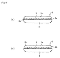
- cross-sectional end peripheries 3a, 3a of the buried silicon oxide layer 3 of the SOI substrate 1 are not buried within the substrate, and are exposed at substrate side surfaces.
- the exposed end peripheries 3a, 3a of the oxide layer 3 are removed by etching.
- those cross-sectional end surfaces 2b of the SOI layer 2a corresponding to an upper layer are brought into an overhung state like a canopy, as shown in FIG. 8(b).
- these overhung portions 2b, 2b have such a small thickness on the order of 0.05 to 0.3 ⁇ m, these portions are poor in mechanical strength and are chipped and/or peeled off during subsequent processes. Silicon fragments caused thereby become particles which adhere onto the surface of the SOI layer 2a as the active area. Devices formed on the SOI layer 2a having adhered particles lead to a cause of defects such as of patterning and in various deposition films, thereby problematically lowering a product yield.
- marking characters 16a are provided in a marking character area 16 at an end periphery of one of the main surfaces of a substrate 11.
- oxygen ions I are dosed into the interior of the silicon substrate 2 similarly to the aforementioned SIMOX method, followed by an anneal processing at a higher temperature so as to form a buried silicon oxide layer 3 in a region at a predetermined depth from the surface of the silicon substrate 2.
- the marking characters by laser irradiation generally reach a depth of about 1 ⁇ m from the substrate surface. Further, the buried silicon oxide layer is formed at a sub-micron depth from the substrate surface.
- the marking character portion and the buried oxide layer overlap with each other, thereby causing a problem of dust occurrence from the marking character portion.
- the invention of claim 1 as shown in FIG. 1 is a manufacturing method of a SOI substrate comprising the steps of: forming an oxide film 12 at cross-sectional both main surfaces and both end surfaces of a silicon substrate 11; forming a resist layer 13 on the oxide film 12 at cross-sectional both end surfaces of the substrate 11; removing the oxide film 12 at those portions which are left from the covering of the resist layer 13, to thereby expose the both main surfaces of the silicon substrate 11; removing the resist layer 13 to thereby leave the oxide film 12 at the both end surfaces of the substrate 11; dosing oxygen ions I into the substrate 11 from one of the exposed both main surfaces, followed by an anneal processing to thereby form an oxide layer 14 in a region at a predetermined depth from the one main surface of the substrate 11; and removing the oxide film 12 left on the both end surfaces of the substrate 11.
- oxygen ions I are dosed into the exposed silicon substrate 11 in a state where the resist layer 13 is removed from the oxide film 12, and the anneal processing is conducted.
- impurities such as metal into the SOI layer 11a as an active area.
- dust occurrence from the end surfaces of the SOI layer 11a as the active area can be avoided during the subsequent device manufacturing process so that contamination due to particles onto the surface of the device is avoided.
- the invention of claim 2 as shown in FIGS. 4 and 5 is a manufacturing method of a SOI substrate of claim 1, wherein the silicon substrate 11 includes a marking character area 16 for carrying marking characters for identifying the substrate 11 at an end periphery of the one of the both main surfaces of the substrate 11, and wherein the resist layer 13 covers the marking character area 16, when the resist layer 13 is formed on the oxide film 12 at the both end surfaces of the substrate 11.
- the marking character area 16 is not exposed during the oxide film removing process.
- the buried silicon oxide layer 14 is not formed under the marking character area 16, thereby enabling avoidance of dust occurrence due to marking characters.
- the invention according to claim 4 as shown in FIG. 6 is a manufacturing method of a SOI substrate comprising the steps of: forming an oxide film 12 at cross-sectional both main surfaces and cross-sectional both end surfaces of a silicon substrate 11; removing the oxide film 12 at one of the both main surfaces of the silicon substrate 11 to thereby expose the one main surface of the substrate 11; dosing oxygen ions I into the substrate 11 from the exposed one main surface, followed by an anneal processing to thereby form an oxide layer 14 in a region at a predetermined depth from the one main surface of the substrate 11; and removing the oxide film 12 left on the other main surface and the both end surfaces of the substrate 11.
- the invention of claim 5 is a manufacturing method of a SOI substrate of claim 4, wherein removal of the oxide film 12 on the one main surface of the silicon substrate 11 is conducted by contacting only the one main surface of the silicon substrate 11 with a hydrofluoric acid aqueous solution 21 while rotating the silicon substrate 11.
- the process to form the resist layer in the invention according to claim 1 is not required, so that ion dosing is conducted after more readily coating the cross-sectional end surfaces of the substrate.
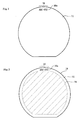
- the invention of claim 6 is a SOI substrate free of a buried silicon oxide layer 14 just under marking characters 16a attached to the substrate surface for substrate identification.
- the marking characters 16a and the buried silicon oxide layer 14 never overlap with each other, thereby avoiding dust occurrence due to marking characters.
- the invention of claim 7 is a semiconductor device adopting a SOI substrate free of a buried silicon oxide layer 14 just under marking characters 16a attached to the substrate surface for substrate identification.
- the invention of claim 8 is a semiconductor device adopting a SOI substrate manufactured by a method of claim 1 or 3.
- the invention of claim 9 is a semiconductor device adopting a SOI substrate manufactured by a method of claim 4 or 5.
- the semiconductor device adopts a SOI substrate having extremely lesser adherence such as of particles and impurities onto a SOI layer as an active area, leading to extremely lesser defects such as of patterning and in various deposition films.
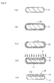
- FIG. 1 There will be firstly described a first embodiment of the present invention, based on FIG. 1.
- a substrate 11 (FIG. 1(a))
- an oxide film 12 is formed by a thermal oxidation method or chemical vapor deposition (CVD) method onto the whole surface, i.e., cross-sectional both main surfaces and both end surfaces (FIG. 1(b)).
- CVD chemical vapor deposition
- a resist is coated onto the oxide film 12 only at both end surfaces of the substrate 11, to thereby form a resist layer 13 on the oxide film 12 (FIG. 1(c)).
- the oxide film 12 is removed at portions not coated with the resist layer 13, to thereby expose both main surfaces of the substrate 11 (FIG. 1(d)).
- the oxide film 12 As means for removing the oxide film 12, there is preferably adopted a method to immerse the substrate 11 into a hydrofluoric acid aqueous solution. Next, the resist layer 13 is removed to thereby leave the oxide film 12 only at both end surfaces of the substrate 11 (FIG. 1(e)). Then, oxygen ions I are dosed into the substrate 11 from one of the exposed main surfaces of the substrate 11, followed by an anneal processing to thereby form a buried silicon oxide layer 14 in a region at a predetermined depth from the one main surface, so as to form a SOI layer 11a as an active area on the oxide layer 14 (FIG. 1(f)).
- the dosage of oxygen ion is in a range from 0.4 x 10 18 /cm 2 to 1.8 x 10 18 /cm 2
- the anneal processing is conducted in an atmosphere of a mixed gas of argon and oxygen at a temperature of 1,300°C to 1,390 °C for 4 to 8 hours.
- the oxide film 12 left at the both end surfaces of the substrate 11 are removed by immersing the oxide film 12 into a hydrofluoric acid aqueous solution, to thereby obtain a desired SOI substrate 10 (FIG. 1(g) and FIG. 1(h)).
- FIG. 1(h) shows an A-A cross-sectional view of FIG. 1(g).
- the resist layer 13 at the cross-sectional both end surfaces of the substrate 11 alternatively to the aforementioned method to coat a resist only at the both end surfaces of the substrate, it is possible to coat a resist to thereby form a resist layer on the whole surface of a substrate (not shown), i.e., on both main surfaces and both end surfaces, then to cover the surface of the resist layer by a pattern mask, and thereafter to conduct exposure and development, to thereby leave the resist layer on the oxide film only at the both end surfaces of the substrate.
- SOG coating spin on glass coating
- SiO x silicon oxide
- FIG. 4 and FIG. 5 show a second embodiment of the present invention.
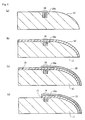
- a silicon substrate 11 having a marking character area 16 (FIG. 4(a)), and an oxide film 12 is formed on the whole surface of the silicon substrate 11, i.e., cross-sectional both main surfaces and both end surfaces thereof (FIG. 4(b)). Then, a resist is coated onto the oxide film 12 at both end surfaces of the silicon substrate 11, to thereby form a resist layer 13 (FIG. 4(c)).
- the resist layer 13 also coats the marking character area 16 carrying marking characters 16a formed by laser irradiation. That part of the oxide film which is not coated with the resist layer 13 is removed, to thereby expose both main surfaces of the silicon substrate 11 (FIG. 4(d)).
- FIG. 5(a) is a plan view of the SOI substrate manufactured by this embodiment. In this way, there is obtained the SOI substrate which is free of the oxide layer 14 just under the marking characters 16a attached to the substrate surface for substrate identification.
- marking characters when marking characters are to be attached to a main surface of a SOI substrate after the SOI substrate is manufactured, that area intended for marking characters is to be coated by a resist layer before marking.
- a resist layer there is firstly prepared a silicon substrate, and an oxide film is formed on the whole surface, i.e., cross-sectional both main surfaces and both end surfaces of this silicon substrate.
- a resist is coated onto the oxide film at the both end surfaces of the silicon substrate, to thereby form resist layer.
- That area intended for marking characters is also coated by the resist layer upon forming the oxide film at the both end surfaces of the substrate. That oxide film not coated by the resist layer is removed, to thereby expose the both main surfaces of the substrate.
- the resist layer is removed, to thereby leave the oxide film at both end surfaces and the marking character area(s) of the silicon substrate.
- oxygen ions are dosed into the substrate from one of the exposed main surfaces of the substrate, followed by an anneal processing to thereby form a buried silicon oxide layer in a region at a predetermined depth from the one main surface, so as to form a SOI layer as an active area on the oxide layer.
- the oxide film left at the both end surfaces and the area intended for marking characters of the substrate is removed by immersing the oxide film into a hydrofluoric acid aqueous solution, to thereby obtain a desired SOI substrate.
- FIG. 6 shows a third embodiment of the present invention.
- Like reference numerals as used in Fig. 1 are used to denote identical elements in FIG. 6.
- a silicon substrate 11 (FIG. 6(a)) similarly to the situation of FIG. 1(a)
- an oxide film 12 is formed on the whole surface, i.e., cross-sectional both main surfaces and both end surfaces of the silicon substrate 11 (FIG. 6(b)) similarly to the situation of FIG. 1(b).
- the oxide film 12 at one of main surfaces is removed, to thereby expose one main surface of the silicon substrate 11 (FIG. 6(c)).
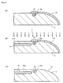
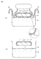
- the silicon substrate 11 formed with the oxide film 12 at the both main surfaces and both end surfaces is arranged above a reservoir 22 filled with a hydrofluoric acid aqueous solution 21 as shown in FIG. 7(a).
- the silicon substrate 11 is then lowered while this substrate 11 is rotated at a low speed by a device (not shown) for rotating, raising and lowering the substrate 11, such that only one main surface corresponding to the lower surface of the substrate 11 is contacted with the hydrofluoric acid aqueous solution 21.
- a carrier gas 23 such as argon is flown from the above of the reservoir 22 onto the upper surface of the carrier gas 23 and onto the hydrofluoric acid aqueous solution 21, as shown by arrows.
- the solution 21 uniformly contacts with the oxide film 12 on the corresponding main surface by virtue of surface tension of the solution 21 as shown in FIG. 7(a), to thereby dissolvingly remove this oxide film 12.
- the carrier gas 23 is flown as shown by the arrows in the drawing, to thereby avoid corrosion of the oxide film 12 at cross-sectional end surfaces of the substrate due to the vapor of the hydrofluoric acid aqueous solution.
- the substrate 11 is kept contacted with the solution 21 for a predetermined period of time, and then the substrate 11 is slowly lifted from the solution 21 while rotating the substrate 11 at a low speed as shown in FIG. 7(b). This provides the substrate 11 one of the main surfaces of which is exposed (FIG. 6(c)).
- oxygen ions I are dosed into the substrate 11 from the exposed main surface of the substrate 11 followed by an anneal processing to thereby form a buried silicon oxide layer 14 in a region at a predetermined depth from the exposed main surface (FIG. 6(d)).
- the oxide film 12 left at the both end surfaces and at the other main surface of the substrate 11 is duly removed, to thereby obtain a desired SOI substrate 10 (FIG. 6(e)).
- FIGS. 10 through 19 show a fourth embodiment of the present invention.
- a semiconductor device making use of the SOI substrate fabricated in the second embodiment.
- Semiconductor devices (hereinafter called "SOI device") each having a SOI structure to be formed on a SOI substrate in which a buried silicon oxide layer and a SOI layer are provided on a silicon substrate, have reduced parasitic capacitance, have features of a high-speed operation and a reduced power consumption, and are used such as in portable devices.
- FIG. 10 shows a partial sectional constitution of a SOI device 30 in which MOS transistors are electrically isolated by trench isolation.
- NMOS transistor N1
- PMOS transistor P-channel type MOS transistor
- Each of the NMOS transistor N1 and PMOS transistor P1 is constituted of a source/drain region SD formed in the SOI layer 33, a channel forming region CH, a gate oxide film GO formed on the channel forming region CH, a gate electrode GT formed on the gate oxide film GO, and a sidewall SW surrounding the side surface of the gate electrode GT.
- the NMOS transistor N1 and PMOS transistor P1 in the SOI device 30 are not only independent of each other by the isolating oxide film 34 in the SOI layer 33, but also fully independent of other semiconductor elements, for example, to thereby present a structure theoretically free of latchup for both transistors.
- FIG. 11 shows a partial sectional constitution of a SOI device 35 having a partial trench isolation structure (PTI structure).
- FIG. 11 there are provided an NMOS transistor N1 and a PMOS transistor P1 on a SOI layer 33, and these transistors are isolated by a partial isolating oxide film 36 provided with a well region WR at its lower portion. Note, the partial isolating oxide film 36 is provided so as to surround the NMOS transistor N1 and PMOS transistor P1.
- an ablation “full trench isolation structure (FTI structure)” is given to a structure where a trench oxide film such as the isolating oxide film 34 in the SOI device 35 reaches the buried silicon oxide layer 32 to thereby electrically and fully isolate elements from one another, and the oxide film of such a structure is called “fully isolating oxide film”.
- FTI structure full trench isolation structure
- the NMOS transistor N1 and PMOS transistor P1 are isolated from each other by the partial isolating oxide film 36. Nonetheless, carriers are allowed to move through the well region WR at the lower portion of the partial isolating oxide film 36, to thereby avoid accumulation of carriers in the channel forming region, and to thereby fix the electric potential of the channel forming region via well region WR, thereby providing such an advantage that various problems due to a substrate floating effect can be avoided.
- a SOI substrate constituted of a silicon substrate 31, a buried silicon oxide layer 32 and a SOI layer 33, in which the buried silicon oxide layer 32 is formed by oxygen ion dosing.
- this SOI substrate is one having no silicon oxide layers just under marking characters 16a attached to the substrate surface for substrate identification.
- the SOI substrate shown in FIG. 3 there can be adopted the SOI substrate shown in FIG. 1(h) or FIG. 6(e), in the semiconductor device of this embodiment.
- the film thickness of the SOI layer 33 is from 50 to 200 nm, and that of the buried silicon oxide layer 32 is from 100 to 400 nm. As shown in FIG.
- an oxide film 38 having a thickness on the order of 10 to 30 nm (100 to 300 Angstrom) is formed on the SOI substrate by a CVD method or thermal oxidation, followed by formation of a nitride film 39 having a thickness of from 30 to 200 nm (300 to 2,000 Angstrom) on the oxide film 38.
- a resist mask RM1 is formed on the nitride film 39, by patterning. This resist mask RM1 has an opening part for forming a trench.
- the nitride film 39, oxide film 38 and SOI layer 33 are patterned by etching by using the resist mask RM1, to thereby form a partial trench TR in the SOI layer 33 as shown in FIG. 13.
- the etching condition is adjusted to leave the SOI layer 33 of a predetermined thickness at the bottom portion of the trench.
- the partial trench TR is formed to extend in a substantially vertical direction with a predetermined width relative to the silicon substrate 31, it becomes possible to isolate elements from each other with keeping fineness and without deteriorating the degree of integration.
- an oxide film having a thickness on the order of 500 nm (5,000 Angstrom) is deposited in the process as shown in FIG. 14, and the oxide film is polished by a CMP (chemical mechanical polishing) processing up to the midway of the nitride film 39. Thereafter, the nitride film 39 and oxide film 38 are removed to thereby form the partial isolating oxide film 36.
- the leftward region in FIG. 14 is supposed to be a first region R1 for forming a transistor of a lower threshold voltage
- the rightward region is supposed to be a second region R2 for forming a transistor having a general threshold voltage and higher reliability.
- an oxide film OX1 is formed over the whole area on the SOI layer 33.
- This oxide film OX1 has a thickness from 1 to 4 nm (10 to 40 Angstrom).
- a resist mask RM2 is formed to cover the second region R2, and semiconductor impurities are doped into the SOI layer 33 via oxide film OX1 by ion dosing.
- the dosing requirement in this case is for forming a transistor having a lower threshold voltage, and if an NMOS transistor is to be formed, for example, boron (B) ion is dosed at an energy of 5 to 40 keV and in a dosage of 1 x 10 11 to 3 x 10 11 /cm 2 .
- boron (B) ion is dosed at an energy of 5 to 40 keV and in a dosage of 1 x 10 11 to 3 x 10 11 /cm 2 .
- boron ion is dosed at an energy of 30 to 100 keV and in a dosage of 1 x
- a resist mask RM3 is formed to cover the first region R1 in the process shown in FIG. 16, and semiconductor impurities are doped into the SOI layer 33 of the second region R2 via oxide film OX1 by ion dosing.
- the dosing requirement in this case is for forming a transistor having a general threshold voltage, and if an NMOS transistor is to be formed, for example, boron (B) ion is dosed at an energy of 5 to 40 keV and in a dosage of 3 x 10 11 to 5 x 10 11 /cm 2 .
- a resist mask RM4 is formed to cover the second region R2 in the process shown in FIG. 17, and the oxide film OX1 in the first region R1 is removed.
- an oxide film is formed over the whole area of the SOI layer as shown in FIG. 18.
- an oxide film OX2 having a thickness of 2 to 4 nm (20 to 40 Angstrom) is formed in the first region R1, and the thickness of the oxide film OX1 is increased to become an oxide film OX3 in the second region R2.
- a polycrystalline silicon layer hereinafter called "polysilicon layer" PS1 intended for a gate electrode is formed over the whole area.
- the polycrystalline silicon layer PS1, oxide films OX2 and OX3 are patterned to form gate electrodes GT1 and GT2 and gate oxide films GO1 and GO2. Further, by forming respective sidewall oxide films SW and source/drain layers SD, NMOS transistors N3 and N4 are formed. Note, the lower portion of the partial isolating oxide film 36 is formed to be the well region WR.
- interlayer insulating films are formed on the NMOS transistors N3, N4 and there is formed a plurality of contact holes which penetrates the interlayer insulating films to thereby reach the source/drain layers SD, these are omitted from the drawing.
- the thus obtained semiconductor device adopts a SOI substrate having a SOI layer substantially free of adhered particles and impurities, leading to extremely lesser defects such as of patterning and in various deposition films.
- a SOI substrate 10 based on the method shown in FIG. 1. Namely, there was prepared an 8-inch substrate 11 having a thickness of 725 ⁇ m, and an oxide film 12 was formed by thermal oxidation on cross-sectional both main surfaces and cross-sectional both end surfaces of this substrate 11. Next, a resist was coated onto the oxide film 12 only at the both end surfaces of the substrate 11 to thereby form a resist layer 13 on the oxide film 12, followed by immersion of the substrate into a buffered hydrofluoric acid solution (BHF solution) so as to remove that portion of oxide film 12 which is not covered by the resist layer 13, thereby exposing the both main surfaces of the substrate 11.
- BHF solution buffered hydrofluoric acid solution
- the resist layer 13 is removed by oxidation by oxygen plasma, to thereby leave the oxide film 12 at both end surfaces of the substrate 11.
- oxygen ions I were dosed into the substrate 11 down to a region at a depth of about 0.4 ⁇ m from one of the exposed both main surfaces of the substrate 11, under the following conditions:
- the substrate 11 was anneal processed in an atmosphere of a mixed gas of argon (99%) and oxygen (1%) at a temperature of 1,350°C for 5 hours, to thereby form an oxide layer 14. Finally, the oxide film 12 left at the both end surfaces of the substrate 11 was removed by immersing the substrate 11 into a hydrofluoric acid aqueous solution, to thereby obtain a desired SOI substrate 10.
- concentrations of metal impurities at surfaces of these SOI substrates were measured. Each concentration of metal impurities was measured, by dropping a mixed acid of hydrofluoric acid and nitric acid onto a central part of a pertinent one of dried SOI substrates, by spreading droplets of the mixed acid over the whole surface of the substrate, and by collecting the droplets for atomic absorption analysis.
- the numbers of particles in the whole surface of the SOI substrates were 20 in the embodiment example 1, 70 in the comparative example 1, and 45 in the comparative example 2. Further, the concentrations of metal impurities in the SOI substrate surface were below a detection limit (below 1 x 10 9 atoms/cm 2 ) concerning Al, Fe, Ni Cu and Zn in the embodiment example 1 and comparative example 1. Contrary, in the comparative example 2, concentrations of Ni and Cu were below a detection limit, those of Al, Fe and Zn were 1 x 10 11 atoms/cm 2 , 2 x 10 10 atoms/cm 2 , and 5 x 10 9 atoms/cm 2 , respectively.
- the manufacturing method of a SOI substrate buried with an insulating layer within a silicon substrate avoids adherence of particles caused by silicon fragments and impurities such as metal within a resist, to thereby improve product yield and avoid dust occurrence caused by marking characters. Further, the SOI substrate of the present invention attached with marking characters never causes dust occurrence due to marking characters.
Landscapes
- Element Separation (AREA)
- Thin Film Transistor (AREA)
Abstract
Description
Claims (9)
- A manufacturing method of a SOI substrate comprising the steps of:forming an oxide film (12) at cross-sectional both main surfaces and both end surfaces of a silicon substrate (11);forming a resist layer (13) on said oxide film (12) at cross-sectional both end surfaces of said substrate (11);removing said oxide film (12) at those portions which are left from the covering of said resist layer (13), to thereby expose said both main surfaces of said silicon substrate (11);removing said resist layer (13) to thereby leave said oxide film (12) at said both end surfaces of said substrate (11);dosing oxygen ions (I) into said substrate (11) from one of said exposed both main surfaces, followed by an anneal processing to thereby form an oxide layer (14) in a region at a predetermined depth from said one main surface of said substrate (11); andremoving said oxide film (12) left on said both end surfaces of said substrate (11).
- A manufacturing method of a SOI substrate of claim 1,wherein said silicon substrate (11) includes a marking character area (16) for carrying marking characters for identifying said substrate (11) at an end periphery of said one of said both main surfaces of said substrate (11), andwherein said resist layer (13) covers said marking character area (16), when said resist layer (13) is formed on said oxide film (12) at said both end surfaces of said substrate (11).
- A manufacturing method of a SOI substrate of claim 1 or 2,
wherein removal of said oxide film (12) is conducted by immersing said substrate (11) into a hydrofluoric acid aqueous solution. - A manufacturing method of a SOI substrate comprising the steps of:forming an oxide film (12) at cross-sectional both main surfaces and cross-sectional both end surfaces of a silicon substrate (11);removing said oxide film (12) at one of said both main surfaces of said silicon substrate (11) to thereby expose said one main surface of said substrate (11);dosing oxygen ions (I) into said substrate (11) from said exposed one main surface, followed by an anneal processing to thereby form an oxide layer (14) in a region at a predetermined depth from said one main surface of said substrate (11); andremoving said oxide film (12) left on the other main surface and said both end surfaces of said substrate (11).
- A manufacturing method of a SOI substrate of claim 4,
wherein removal of said oxide film (12) on said one main surface of said silicon substrate (11) is conducted by contacting only said one main surface of said silicon substrate (11) with a hydrofluoric acid aqueous solution (21) while rotating said silicon substrate (11). - A SOI substrate free of a buried silicon oxide layer (14) just under marking characters (16a) attached to the substrate surface for substrate identification.
- A semiconductor device adopting a SOI substrate free of a buried silicon oxide layer (14) just under marking characters (16a) attached to the substrate surface for substrate identification.
- A semiconductor device adopting a SOI substrate manufactured by a method of claim 1 or 3.
- A semiconductor device adopting a SOI substrate manufactured by a method of claim 4 or 5.
Applications Claiming Priority (3)
| Application Number | Priority Date | Filing Date | Title |
|---|---|---|---|
| JP18910099 | 1999-07-02 | ||
| JP18910099 | 1999-07-02 | ||
| PCT/JP2000/004376 WO2001003191A1 (en) | 1999-07-02 | 2000-06-30 | Soi substrate, method of manufacture thereof, and semiconductor device using soi substrate |
Publications (3)
| Publication Number | Publication Date |
|---|---|
| EP1122788A1 true EP1122788A1 (en) | 2001-08-08 |
| EP1122788A4 EP1122788A4 (en) | 2006-05-17 |
| EP1122788B1 EP1122788B1 (en) | 2009-03-25 |
Family
ID=16235363
Family Applications (1)
| Application Number | Title | Priority Date | Filing Date |
|---|---|---|---|
| EP00942438A Expired - Lifetime EP1122788B1 (en) | 1999-07-02 | 2000-06-30 | Method of manufacturing of an soi substrate |
Country Status (4)
| Country | Link |
|---|---|
| US (1) | US6558990B1 (en) |
| EP (1) | EP1122788B1 (en) |
| DE (1) | DE60041863D1 (en) |
| WO (1) | WO2001003191A1 (en) |
Cited By (2)
| Publication number | Priority date | Publication date | Assignee | Title |
|---|---|---|---|---|
| FR2834125A1 (en) * | 2001-12-20 | 2003-06-27 | Mitsubishi Electric Corp | SEMICONDUCTOR DEVICE COMPRISING A TRENCH INSULATOR AND METHOD FOR MANUFACTURING THE DEVICE |
| FR2835967A1 (en) * | 2002-02-14 | 2003-08-15 | Mitsubishi Electric Corp | SEMICONDUCTOR DEVICE, MANUFACTURING METHOD, AND SEMICONDUCTOR WAFER |
Families Citing this family (2)
| Publication number | Priority date | Publication date | Assignee | Title |
|---|---|---|---|---|
| JP4902953B2 (en) * | 2004-09-30 | 2012-03-21 | ラピスセミコンダクタ株式会社 | Manufacturing method of semiconductor device |
| JP5618521B2 (en) * | 2008-11-28 | 2014-11-05 | 株式会社半導体エネルギー研究所 | Method for manufacturing semiconductor device |
Family Cites Families (13)
| Publication number | Priority date | Publication date | Assignee | Title |
|---|---|---|---|---|
| NL8701251A (en) * | 1987-05-26 | 1988-12-16 | Philips Nv | SEMICONDUCTOR DEVICE AND METHOD OF MANUFACTURE THEREOF |
| JPS63312632A (en) | 1987-06-15 | 1988-12-21 | Nec Corp | Manufacture of semiconductor device |
| JPH0279445A (en) * | 1988-09-14 | 1990-03-20 | Oki Electric Ind Co Ltd | Forming method of element isolating region |
| JPH04129267A (en) * | 1990-09-20 | 1992-04-30 | Fujitsu Ltd | Semiconductor substrate and manufacture thereof |
| JP2998330B2 (en) * | 1991-09-19 | 2000-01-11 | 日本電気株式会社 | SIMOX substrate and method of manufacturing the same |
| JPH05259011A (en) * | 1992-03-16 | 1993-10-08 | Fujitsu Ltd | Semiconductor device and manufacturing method thereof |
| JP3272517B2 (en) * | 1993-12-01 | 2002-04-08 | 三菱電機株式会社 | Method for manufacturing semiconductor device |
| JPH07176608A (en) | 1993-12-17 | 1995-07-14 | Nec Corp | Semiconductor device and manufacturing method thereof |
| JP3745392B2 (en) * | 1994-05-26 | 2006-02-15 | 株式会社ルネサステクノロジ | Semiconductor device |
| JP2870492B2 (en) | 1995-09-28 | 1999-03-17 | 日本電気株式会社 | SOI substrate and manufacturing method thereof |
| US5869386A (en) * | 1995-09-28 | 1999-02-09 | Nec Corporation | Method of fabricating a composite silicon-on-insulator substrate |
| KR100253699B1 (en) * | 1996-06-29 | 2000-05-01 | 김영환 | Soi device and its manufacturing method |
| JPH11204452A (en) | 1998-01-13 | 1999-07-30 | Mitsubishi Electric Corp | Semiconductor substrate processing method and semiconductor substrate |
-
2000
- 2000-06-30 WO PCT/JP2000/004376 patent/WO2001003191A1/en not_active Ceased
- 2000-06-30 US US09/786,228 patent/US6558990B1/en not_active Expired - Lifetime
- 2000-06-30 DE DE60041863T patent/DE60041863D1/en not_active Expired - Lifetime
- 2000-06-30 EP EP00942438A patent/EP1122788B1/en not_active Expired - Lifetime
Cited By (5)
| Publication number | Priority date | Publication date | Assignee | Title |
|---|---|---|---|---|
| FR2834125A1 (en) * | 2001-12-20 | 2003-06-27 | Mitsubishi Electric Corp | SEMICONDUCTOR DEVICE COMPRISING A TRENCH INSULATOR AND METHOD FOR MANUFACTURING THE DEVICE |
| US7183167B2 (en) | 2001-12-20 | 2007-02-27 | Renesas Technology Corp. | Semiconductor device having a trench isolation and method of fabricating the same |
| US7494883B2 (en) | 2001-12-20 | 2009-02-24 | Renesas Technology Corp. | Semiconductor device having a trench isolation and method of fabricating the same |
| FR2835967A1 (en) * | 2002-02-14 | 2003-08-15 | Mitsubishi Electric Corp | SEMICONDUCTOR DEVICE, MANUFACTURING METHOD, AND SEMICONDUCTOR WAFER |
| FR2835968A1 (en) * | 2002-02-14 | 2003-08-15 | Mitsubishi Electric Corp | SEMICONDUCTOR DEVICE, MANUFACTURING METHOD, AND SEMICONDUCTOR WAFER |
Also Published As
| Publication number | Publication date |
|---|---|
| EP1122788A4 (en) | 2006-05-17 |
| EP1122788B1 (en) | 2009-03-25 |
| DE60041863D1 (en) | 2009-05-07 |
| US6558990B1 (en) | 2003-05-06 |
| WO2001003191A1 (en) | 2001-01-11 |
Similar Documents
| Publication | Publication Date | Title |
|---|---|---|
| JP2004047952A (en) | Semiconductor device and manufacturing method thereof | |
| US7442652B2 (en) | Method for removing contamination and method for fabricating semiconductor device | |
| US6727187B2 (en) | Fabrication method for semiconductor device | |
| Heyns et al. | Cost-effective cleaning and high-quality thin gate oxides | |
| EP0690484A1 (en) | Method of manufacturing semiconductor device and methods of processing, analyzing and manufacturing its substrate | |
| KR100547547B1 (en) | Stencil mask having an antistatic function and method of manufacturing the same | |
| US6558990B1 (en) | SOI substrate, method of manufacture thereof, and semiconductor device using SOI substrate | |
| CN111247628B (en) | Method for manufacturing semiconductor device | |
| US9129796B2 (en) | Pre-metal deposition clean process | |
| US8598004B2 (en) | Self aligned MOS structure with polysilicon contact | |
| TWI628718B (en) | Glass with depleted layer and polycrystalline germanium film transistor built thereon | |
| EP2533283A1 (en) | Semiconductor device and manufacturing method therefor | |
| JP2000114397A (en) | Manufacture of semiconductor device | |
| CN114446996B (en) | Co-integrated high voltage (HV) and medium voltage (MV) field effect transistors with defect-proof structures | |
| EP1655774A2 (en) | Method of manufacturing a MOSFET | |
| JPWO2001003191A1 (en) | SOI substrate, its manufacturing method, and semiconductor device using the same | |
| US10262909B2 (en) | Semiconductor device and method for manufacturing the same | |
| US20070026584A1 (en) | Dielectric isolated body biasing of silicon on insulator | |
| US7026198B2 (en) | Focused ion beam treatment method and semiconductor device suitable for its implementation | |
| WO2009084284A1 (en) | Insulating substrate for semiconductor device, semiconductor device, and method for manufacturing semiconductor device | |
| CN119340228A (en) | Method and test structure for evaluating metal contamination in wafer processes | |
| US20130037816A1 (en) | Semiconductor device and manufacturing method thereof | |
| Goodner et al. | Investigation of rod-like defects in MOS 12 | |
| JPH10233402A (en) | Method for manufacturing semiconductor device | |
| JPH0964367A (en) | Semiconductor device and manufacturing method thereof |
Legal Events
| Date | Code | Title | Description |
|---|---|---|---|
| PUAI | Public reference made under article 153(3) epc to a published international application that has entered the european phase |
Free format text: ORIGINAL CODE: 0009012 |
|
| 17P | Request for examination filed |
Effective date: 20010402 |
|
| AK | Designated contracting states |
Kind code of ref document: A1 Designated state(s): AT BE CH CY DE DK ES FI FR GB GR IE IT LI LU MC NL PT SE |
|
| RBV | Designated contracting states (corrected) |
Designated state(s): DE FR |
|
| RAP1 | Party data changed (applicant data changed or rights of an application transferred) |
Owner name: MITSUBISHI DENKI KABUSHIKI KAISHA Owner name: MITSUBISHI MATERIALS SILICON CORPORATION |
|
| A4 | Supplementary search report drawn up and despatched |
Effective date: 20060405 |
|
| RIC1 | Information provided on ipc code assigned before grant |
Ipc: H01L 27/12 20060101ALI20060330BHEP Ipc: H01L 21/762 20060101AFI20060330BHEP Ipc: H01L 21/265 20060101ALI20060330BHEP |
|
| 17Q | First examination report despatched |
Effective date: 20060821 |
|
| RTI1 | Title (correction) |
Free format text: METHOD OF MANUFACTURING OF AN SOI SUBSTRATE |
|
| GRAP | Despatch of communication of intention to grant a patent |
Free format text: ORIGINAL CODE: EPIDOSNIGR1 |
|
| GRAS | Grant fee paid |
Free format text: ORIGINAL CODE: EPIDOSNIGR3 |
|
| GRAA | (expected) grant |
Free format text: ORIGINAL CODE: 0009210 |
|
| AK | Designated contracting states |
Kind code of ref document: B1 Designated state(s): DE FR |
|
| REF | Corresponds to: |
Ref document number: 60041863 Country of ref document: DE Date of ref document: 20090507 Kind code of ref document: P |
|
| PLBE | No opposition filed within time limit |
Free format text: ORIGINAL CODE: 0009261 |
|
| STAA | Information on the status of an ep patent application or granted ep patent |
Free format text: STATUS: NO OPPOSITION FILED WITHIN TIME LIMIT |
|
| 26N | No opposition filed |
Effective date: 20091229 |
|
| REG | Reference to a national code |
Ref country code: FR Ref legal event code: TQ |
|
| REG | Reference to a national code |
Ref country code: DE Ref legal event code: R082 Ref document number: 60041863 Country of ref document: DE Representative=s name: BARDEHLE PAGENBERG PARTNERSCHAFT MBB PATENTANW, DE |
|
| REG | Reference to a national code |
Ref country code: DE Ref legal event code: R082 Ref document number: 60041863 Country of ref document: DE Representative=s name: BARDEHLE PAGENBERG PARTNERSCHAFT MBB PATENTANW, DE Effective date: 20140915 Ref country code: DE Ref legal event code: R081 Ref document number: 60041863 Country of ref document: DE Owner name: RENESAS ELECTRONICS CORPORATION, KAWASAKI-SHI, JP Free format text: FORMER OWNER: MITSUBISHI MATERIALS SILICON CO, MITSUBISHI DENKI K.K., , JP Effective date: 20140915 Ref country code: DE Ref legal event code: R081 Ref document number: 60041863 Country of ref document: DE Owner name: MITSUBISHI MATERIALS SILICON CORP., JP Free format text: FORMER OWNER: MITSUBISHI MATERIALS SILICON CO, MITSUBISHI DENKI K.K., , JP Effective date: 20140915 Ref country code: DE Ref legal event code: R081 Ref document number: 60041863 Country of ref document: DE Owner name: RENESAS ELECTRONICS CORPORATION, JP Free format text: FORMER OWNERS: MITSUBISHI MATERIALS SILICON CORP., TOKIO/TOKYO, JP; MITSUBISHI DENKI K.K., TOKYO, JP Effective date: 20140915 Ref country code: DE Ref legal event code: R081 Ref document number: 60041863 Country of ref document: DE Owner name: MITSUBISHI MATERIALS SILICON CORP., JP Free format text: FORMER OWNERS: MITSUBISHI MATERIALS SILICON CORP., TOKIO/TOKYO, JP; MITSUBISHI DENKI K.K., TOKYO, JP Effective date: 20140915 Ref country code: DE Ref legal event code: R081 Ref document number: 60041863 Country of ref document: DE Owner name: RENESAS ELECTRONICS CORPORATION, KAWASAKI-SHI, JP Free format text: FORMER OWNERS: MITSUBISHI MATERIALS SILICON CORP., TOKIO/TOKYO, JP; MITSUBISHI DENKI K.K., TOKYO, JP Effective date: 20140915 |
|
| REG | Reference to a national code |
Ref country code: FR Ref legal event code: PLFP Year of fee payment: 17 |
|
| REG | Reference to a national code |
Ref country code: FR Ref legal event code: PLFP Year of fee payment: 18 |
|
| REG | Reference to a national code |
Ref country code: DE Ref legal event code: R082 Ref document number: 60041863 Country of ref document: DE Representative=s name: BARDEHLE PAGENBERG PARTNERSCHAFT MBB PATENTANW, DE Ref country code: DE Ref legal event code: R081 Ref document number: 60041863 Country of ref document: DE Owner name: RENESAS ELECTRONICS CORPORATION, JP Free format text: FORMER OWNERS: MITSUBISHI MATERIALS SILICON CORP., TOKIO/TOKYO, JP; RENESAS ELECTRONICS CORPORATION, KAWASAKI-SHI, KANAGAWA, JP Ref country code: DE Ref legal event code: R081 Ref document number: 60041863 Country of ref document: DE Owner name: MITSUBISHI MATERIALS SILICON CORP., JP Free format text: FORMER OWNERS: MITSUBISHI MATERIALS SILICON CORP., TOKIO/TOKYO, JP; RENESAS ELECTRONICS CORPORATION, KAWASAKI-SHI, KANAGAWA, JP |
|
| REG | Reference to a national code |
Ref country code: FR Ref legal event code: TQ Owner name: MITSUBISHI MATERIALS SILICON CORP Effective date: 20171114 Ref country code: FR Ref legal event code: TQ Owner name: RENESAS ELECTRONICS CORPORATION, JP Effective date: 20171114 |
|
| REG | Reference to a national code |
Ref country code: DE Ref legal event code: R082 Ref document number: 60041863 Country of ref document: DE Representative=s name: BARDEHLE PAGENBERG PARTNERSCHAFT MBB PATENTANW, DE Ref country code: DE Ref legal event code: R081 Ref document number: 60041863 Country of ref document: DE Owner name: RENESAS ELECTRONICS CORPORATION, JP Free format text: FORMER OWNERS: MITSUBISHI MATERIALS SILICON CORP., TOKIO/TOKYO, JP; RENESAS ELECTRONICS CORPORATION, TOKIO/TOKYO, JP Ref country code: DE Ref legal event code: R081 Ref document number: 60041863 Country of ref document: DE Owner name: MITSUBISHI MATERIALS SILICON CORP., JP Free format text: FORMER OWNERS: MITSUBISHI MATERIALS SILICON CORP., TOKIO/TOKYO, JP; RENESAS ELECTRONICS CORPORATION, TOKIO/TOKYO, JP |
|
| REG | Reference to a national code |
Ref country code: FR Ref legal event code: CA Effective date: 20171120 Ref country code: FR Ref legal event code: CD Owner name: MITSUBISHI MATERIALS SILICON CORP Effective date: 20171120 Ref country code: FR Ref legal event code: CD Owner name: RENESAS ELECTRONICS CORPORATION, JP Effective date: 20171120 |
|
| REG | Reference to a national code |
Ref country code: FR Ref legal event code: PLFP Year of fee payment: 19 |
|
| PGFP | Annual fee paid to national office [announced via postgrant information from national office to epo] |
Ref country code: DE Payment date: 20190619 Year of fee payment: 20 |
|
| PGFP | Annual fee paid to national office [announced via postgrant information from national office to epo] |
Ref country code: FR Payment date: 20190619 Year of fee payment: 20 |
|
| REG | Reference to a national code |
Ref country code: DE Ref legal event code: R071 Ref document number: 60041863 Country of ref document: DE |