EP1122713A2 - Circuit LSI de traitement d'image comportant une mémoire, système de traitement d'image comportant ce circuit et méthode d'accès à une image utilisant ce circuit - Google Patents
Circuit LSI de traitement d'image comportant une mémoire, système de traitement d'image comportant ce circuit et méthode d'accès à une image utilisant ce circuit Download PDFInfo
- Publication number
- EP1122713A2 EP1122713A2 EP20010102174 EP01102174A EP1122713A2 EP 1122713 A2 EP1122713 A2 EP 1122713A2 EP 20010102174 EP20010102174 EP 20010102174 EP 01102174 A EP01102174 A EP 01102174A EP 1122713 A2 EP1122713 A2 EP 1122713A2
- Authority
- EP
- European Patent Office
- Prior art keywords
- memory
- word
- page
- image
- power consumption
- Prior art date
- Legal status (The legal status is an assumption and is not a legal conclusion. Google has not performed a legal analysis and makes no representation as to the accuracy of the status listed.)
- Withdrawn
Links
Images


Classifications
-
- H—ELECTRICITY
- H04—ELECTRIC COMMUNICATION TECHNIQUE
- H04N—PICTORIAL COMMUNICATION, e.g. TELEVISION
- H04N19/00—Methods or arrangements for coding, decoding, compressing or decompressing digital video signals
- H04N19/42—Methods or arrangements for coding, decoding, compressing or decompressing digital video signals characterised by implementation details or hardware specially adapted for video compression or decompression, e.g. dedicated software implementation
- H04N19/423—Methods or arrangements for coding, decoding, compressing or decompressing digital video signals characterised by implementation details or hardware specially adapted for video compression or decompression, e.g. dedicated software implementation characterised by memory arrangements
-
- G—PHYSICS
- G09—EDUCATION; CRYPTOGRAPHY; DISPLAY; ADVERTISING; SEALS
- G09G—ARRANGEMENTS OR CIRCUITS FOR CONTROL OF INDICATING DEVICES USING STATIC MEANS TO PRESENT VARIABLE INFORMATION
- G09G5/00—Control arrangements or circuits for visual indicators common to cathode-ray tube indicators and other visual indicators
- G09G5/36—Control arrangements or circuits for visual indicators common to cathode-ray tube indicators and other visual indicators characterised by the display of a graphic pattern, e.g. using an all-points-addressable [APA] memory
- G09G5/39—Control of the bit-mapped memory
-
- H—ELECTRICITY
- H04—ELECTRIC COMMUNICATION TECHNIQUE
- H04N—PICTORIAL COMMUNICATION, e.g. TELEVISION
- H04N19/00—Methods or arrangements for coding, decoding, compressing or decompressing digital video signals
- H04N19/60—Methods or arrangements for coding, decoding, compressing or decompressing digital video signals using transform coding
- H04N19/61—Methods or arrangements for coding, decoding, compressing or decompressing digital video signals using transform coding in combination with predictive coding
-
- G—PHYSICS
- G09—EDUCATION; CRYPTOGRAPHY; DISPLAY; ADVERTISING; SEALS
- G09G—ARRANGEMENTS OR CIRCUITS FOR CONTROL OF INDICATING DEVICES USING STATIC MEANS TO PRESENT VARIABLE INFORMATION
- G09G2330/00—Aspects of power supply; Aspects of display protection and defect management
- G09G2330/02—Details of power systems and of start or stop of display operation
- G09G2330/021—Power management, e.g. power saving
-
- G—PHYSICS
- G09—EDUCATION; CRYPTOGRAPHY; DISPLAY; ADVERTISING; SEALS
- G09G—ARRANGEMENTS OR CIRCUITS FOR CONTROL OF INDICATING DEVICES USING STATIC MEANS TO PRESENT VARIABLE INFORMATION
- G09G2360/00—Aspects of the architecture of display systems
- G09G2360/12—Frame memory handling
- G09G2360/122—Tiling
Definitions
- the present invention relates generally to a memory-consolidated image processing LSI (Large Scale Integrated circuit). More specifically, the invention relates to a memory-consolidated image processing LSI capable of being driven at low power consumption.
- Memory elements consolidated with an image processing part to constitute a memory part include ferroelectric random access memories (FeRAMs), magnetoresistance random access memories (MRAMs) and so forth.
- Conventional memory consolidated image processing LSIs are designed to improve the processing speed for writing or the like, and have been scarcely taken measures to cope with the decrease of the driving power of the LSIs.
- a first power A is first consumed to access the page regions of the storage region of a memory, which comprises a plurality of page regions including a plurality of word regions, and then, a second power B is consumed to access the word regions.
- a second power B is consumed to access the word regions.
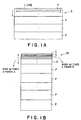
- FIG. 1A shows a display screen S of a display unit, such as a CRT (Cathode Ray Tube) or a liquid crystal display, for displaying, e.g., dynamic image data.
- the display screen S is virtually segmented into a plurality of page regions P.
- Each of the page regions P comprises a plurality of words L, each of which is, e.g., data for one line scanned in a horizontal scanning period (1H).
- the data thus virtually segmented on the display screen are stored in a storage region M of the DRAM shown in FIG. 1B.
- the storage region M comprises a plurality of storage regions P, which correspond to the display screen S, for storing data for one line, and a plurality of word storage regions L, each of which corresponds to data for 1 H to be included in a corresponding one of the storage regions P.
- the conventional memory consolidated image processing LSI is designed to store image data for one frame on the display screen S and data stored in the DRAM so that the image data correspond to the data stored in the DRAM. For that reason, in order to access the DRAM, after the storage region P for each page shown in FIG. 1B is accessed, each word L corresponding to a scanning line is accessed to write or read data.
- the power A for accessing the pages must be multiplied by the number of the pages (P x n times x power A), and the power B for accessing the words must be multiplied by the number of required words (L x m times x power B). Therefore, the whole power consumption increases in proportion to the numbers of accessed pages and words. As a result, if the region of an image, which is required to be processed, extends over a large number of pages, the power consumption for the pages is required.
- a technique called tiling is used for reducing the number of accesses to a DRAM to shorten the access time.
- the tiling is designed to change the reading sequence of data on a display screen S although it does not change the image range.
- the tiling takes account of the fact that the reading time is shorten by simultaneously reading two word data on the same page, wherein word data stored in another page exists therebetween, when the two word data are intended to be read.
- the access speed is improved as the sizes of a page and a word region increase, a larger page size and a larger word size are used.
- the degree of freedom capable of selecting the sizes of a page and a word is small.
- memory consolidated image processing LSIs mounted on portable electronics are often driven by a rechargeable battery.
- the loaded battery may have a large charging capacity so that the LSIs can be used for a long time, this prevents the whole electronics from being miniaturized since the weight increases. Therefore, although the capacity of the loaded battery is determined in view of the weight and size to some extent, it has been requested that the power consumption of the LSI should be saved as small as possible.
- a memory consolidated image processing LSI comprises: a memory part including a page region for storing image data for a plurality of lattice-like page ranges which are formed by segmenting an image plane corresponding to a display screen and each of which has sides a power of 2 long, and word regions, each of which stores image data for a plurality of word ranges formed by segmenting each of the page ranges and which are assembled to constitute the page region; and an image access part for word-accessing the word ranges after accessing the page ranges by a pre-charge in order to access the memory part.
- the page region or word region stored in said memory part is set so as to have a multiplied value of a power consumption per one of pre-charges in a power consumption model of a memory by an average number of the pre-charges to be a substantially minimum value, or a multiplied value of a power consumption per one of word accesses in a power consumption model of a memory by an average number of the word accesses to be a substantially minimum value.
- the substantially minimum value does not mean that the multiplied value completely coincides with the absolutely minimum value, and means that the multiplied value includes proximity values of the minimum value.
- the page ranges on the image plane wherein image data is stored in the page region of the memory part has a size so that the multiplied value of power consumption per one of the pre-charges in a power consumption model of a memory by an average number of pre-charges is the substantially minimum value.
- the word ranges on the image plane wherein image data is stored in the word region of the memory part has a size so that the multiplied value of a power consumption per one of the word accesses in a power consumption model of a memory by an average number of word accesses is the substantially minimum value.
- the page ranges on the image plane wherein image data is stored in the page region of the memory part has a size so that the multiplied value of a power consumption per one of the pre-charges in a power consumption model of a memory by an average number of pre-charges is the substantially minimum value
- the word ranges on the image plane wherein image data is stored in the word region of the memory part has a size so that the multiplied value of a power consumption per one of the word accesses in a power consumption model of a memory by an average number of word accesses is the substantially minimum value.
- the image plane may comprise a plurality of pixels, and the page ranges are formed by segmenting the image plane into rectangular ranges with sides 8 to 16 pixels long or in a rectangular range which has a size approximating to that of the square range and which has an aspect ratio of up to 1 : 2.
- a two-dimensional plane which has been stored in the memory region, may be segmented into square areas having the same capacity as that of the page range or rectangular areas with sides of a ratio of 1 : 2 to be collectively stored in separate page regions.
- the image plane may comprise a plurality of pixels
- the word ranges may be formed by segmenting the image plane into rectangular ranges with sides 8 to 16 pixels long or in a rectangular range which has a size approximating to that of the square range and which has an aspect ratio of up to 1 : 2.
- a two-dimensional plane which has been stored in the memory region, may be segmented into square areas having the same capacity as that of the page range or rectangular areas with sides of a ratio of 1 : 2 to be collectively stored in separate page regions.
- the memory part may comprise a dynamic random access memory (DRAM).
- the memory part may comprise a ferroelectric random access memory (FeRAM).
- the memory part may comprise a magnetoresistance random access memory (MRAM).
- the image access part may be a circuit for processing a bit stream based on a dynamic image compressing standard, such as MPEG-4, MPEG-2, MPEG-1 or H.263, and the memory part may be a memory having a unit for the preparation for reading, i.e., a region corresponding to the page region in a DRAM, the size of the page range on the image plane being preferably in the range of from 64 pixels to 512 pixels, or in the range of from 512 pixels to 1024 pixels.
- a dynamic image compressing standard such as MPEG-4, MPEG-2, MPEG-1 or H.263
- the memory part may be a memory having a unit for the preparation for reading, i.e., a region corresponding to the page region in a DRAM, the size of the page range on the image plane being preferably in the range of from 64 pixels to 512 pixels, or in the range of from 512 pixels to 1024 pixels.
- the image access part may be a circuit for processing a bit stream based on a dynamic image compressing standard, such as MPEG-4, MPEG-2, MPEG-1 or H.263, and the memory part may be a memory having a unit corresponding to a data bus, i.e., the word region corresponding to a word region in a DRAM, the size of the word range on the image plane being preferably in the range of from 8 pixels to 64 pixels, or in the range of from 64 pixels to 256 pixels.
- a dynamic image compressing standard such as MPEG-4, MPEG-2, MPEG-1 or H.263
- the memory part may be a memory having a unit corresponding to a data bus, i.e., the word region corresponding to a word region in a DRAM, the size of the word range on the image plane being preferably in the range of from 8 pixels to 64 pixels, or in the range of from 64 pixels to 256 pixels.
- an image processing system having an image compressing and/or expanding unit for compressing and/or expanding image information includes a memory consolidated image processing LSI comprising: a memory part having a plurality of lattice-like page ranges for storing the image data of the page ranges which are formed by segmenting an image plane corresponding to a display screen and each of which has sides a power of 2 long, and a plurality of word ranges for storing the image data of the word ranges which are formed by segmenting each of the page ranges and which are assembled to constitute each of the page ranges; and an image access part for accessing the word ranges after accessing the page ranges by a pre-charge in order to access the memory part.
- each of the page ranges and each of the word ranges in the memory part of the memory consolidated image processing LSI may be set to be a desired page range and a desired word range, which allow desired image data to be accessed at the minimum power consumption by the minimum number of pre-charges and the minimum number of charges.
- the image processing system may further comprise: a raster converting part for raster-converting the image information; and a processing part for converting the image data, which has been converted by the raster converting part, into data corresponding to the desired page and word ranges, wherein the memory consolidated image processing LSI stores the image data for the desired page and word ranges, which has been converted by the processing part, in the page and word regions of the memory part, and the image access part accesses by word-accessing the desired word region after being pre-charged in the desired page region of the memory part.
- the image processing system may further comprise: a raster converting part for raster-converting the image information; a temporary memory part for temporarily storing the image data which has been converted by the raster converting part; and a processing part for converting the image data, which has been stored in the temporary memory part, into data corresponding to the desired page and word ranges, wherein the memory consolidated image processing LSI stores the desired page and word ranges, which have been converted by the processing part, in the page and word regions of the memory part, and the image access part accesses the desired word region after being pre-charged in the desired page region of the memory part.
- the image processing system may further comprise an MPEG processing part for compression-coding image data using an MPEG coding system, wherein the memory consolidated image processing LSI stores the desired page and word ranges for the image data, which has been processed by the MPEG processing part, in the memory part, and the image access part accesses by word-accessing the desired word region after being pre-charged in the desired page range of the memory part.
- the image access part may be a circuit for processing a bit stream based on a dynamic image compressing standard, such as MPEG-4, MPEG-2, MPEG-1 or H.263, and the memory part may be a memory having the page region corresponding to the page range serving as a unit for the preparation for reading, the size of the page range on the image plane being preferably in the range of from 64 pixels to 512 pixels.
- a dynamic image compressing standard such as MPEG-4, MPEG-2, MPEG-1 or H.263
- the memory part may be a memory having the page region corresponding to the page range serving as a unit for the preparation for reading, the size of the page range on the image plane being preferably in the range of from 64 pixels to 512 pixels.
- the image access part may be a circuit for processing a bit stream based on a dynamic image compressing standard, such as MPEG-4, MPEG-2, MPEG-1 or H.263, and the memory part may be a memory having the page region corresponding to the page range serving as a unit for the preparation for reading, the size of the page range on the image plane being preferably in the range of from 512 pixels to 1024 pixels.
- a dynamic image compressing standard such as MPEG-4, MPEG-2, MPEG-1 or H.263
- the memory part may be a memory having the page region corresponding to the page range serving as a unit for the preparation for reading, the size of the page range on the image plane being preferably in the range of from 512 pixels to 1024 pixels.
- the image access part may be a circuit for processing a bit stream based on a dynamic image compressing standard, such as MPEG-4, MPEG-2, MPEG-1 or H.263, and the memory part may be a memory having the word region corresponding to the word range as a unit corresponding to a data bus, the size of the word range on the image plane being preferably in the range of from 8 pixels to 64 pixels.
- a dynamic image compressing standard such as MPEG-4, MPEG-2, MPEG-1 or H.263
- the memory part may be a memory having the word region corresponding to the word range as a unit corresponding to a data bus, the size of the word range on the image plane being preferably in the range of from 8 pixels to 64 pixels.
- the image access part may be a circuit for processing a bit stream based on a dynamic image compressing standard, such as MPEG-4, MPEG-2, MPEG-1 or H.263, and the memory part may be a memory having the word region corresponding to the word range as a unit corresponding to a data bus, the size of the word range on the image plane being preferably in the range of from 64 pixels to 256 pixels.
- a dynamic image compressing standard such as MPEG-4, MPEG-2, MPEG-1 or H.263
- the memory part may be a memory having the word region corresponding to the word range as a unit corresponding to a data bus, the size of the word range on the image plane being preferably in the range of from 64 pixels to 256 pixels.
- a method for processing image data stored in a memory consolidated image processing LSI which comprises a memory part for storing predetermined image data and having page regions each storing page ranges so that an image plane corresponding to a display screen is segmented into lattice-like ranges each of which has sides a power of 2 long, and a word regions each storing word ranges which are formed by segmenting the page range on the image plane, and an access part for accessing to the memory part in the manner that a multiplied value of a power consumption per one of pre-charges in a power consumption model of a memory by an average number of the pre-charges is a substantially minimum value and that a multiplied value of a power consumption per one of word accesses in a power consumption model of a memory by an average number of the word accesses is a substantially minimum value, the method comprising: a step of accessing in a first stage by pre-charging to the page region of the memory part
- the page region in the memory part is set to have a size so that the multiplied value of the power consumption per one of the pre-charges in a power consumption model of a memory by an average number of pre-charges is the substantially minimum value.
- the word region in the memory part is set to have a size so that the multiplied value of a power consumption per one of word accesses in a power consumption model of a memory by an average number of the word accesses is the substantially minimum value.
- the page region in the memory part is set to have a size so that the multiplied value of the power consumption per one of the pre-charges in a power consumption model of a memory by an average number of pre-charges is the substantially minimum value
- the word region in the memory part is set to have a size so that the multiplied value of a power consumption per one of word accesses in a power consumption model of a memory by an average number of the word accesses is the substantially minimum value.
- a fourth basic construction of the present invention there is provided method for designing a memory consolidated image processing LSI, which comprises a memory part for storing predetermined image data, and an access part for accessing the image data stored in the memory part by using two-stage accesses, in which the method comprises: a step of setting a plurality of page ranges so that an image plane corresponding to a display screen is segmented into lattice-like ranges, each of which has sides a power of 2 long, and so that the multiplied value of the power consumption per one of the pre-charges in a power consumption model of a memory by an average number of pre-charges is the substantially minimum value; a step of setting a page region capable of storing the image data for a page range on the image plane in the memory part; a step of setting a plurality of word ranges which are formed by segmenting the page range on the image plane so that the multiplied value of a power consumption per one of word accesses in a power consumption model of a memory by
- FIGS. 2 through 10 are block, schematic and characteristic diagrams showing the construction, operation and effects of the first preferred embodiment of a memory consolidated image processing LSI according to the present invention.
- a DRAM will be described as an example of a memory.
- the present invention can be applied to other types of memories, such as FeRAMs and MRAMs, which carries out two-stage accesses of a page access and a word access.
- the first preferred embodiment of a memory consolidated image processing LSI is a CODEC LSI for MPEG-4, and comprises an MPEG-4 CODEC 2 and a consolidated DRAM 3.
- the consolidated DRAM 3 is designed to store therein predetermined dynamic image data
- the CODEC 2 is designed to compress and expand the dynamic image data.
- the page size of the consolidated DRAM 3 is 256 bytes per page. However, the page size should not be limited to 256 bytes if it is in the range of from 62 to 512 bytes. For example, the page size may be an image of 128 bytes of "8 x 16" pixels.
- the MPEG-4 CODEC 2 may be another dynamic image compressing or expanding CODEC for carrying out a motion compensation for each macro block or each block, such as MPEG-1, MPEG-2 or H.263.
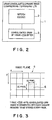
- This CODEC 2 may be another CODEC if it is an image processing circuit capable of accessing a substantially square image of 16 pixels x 16 pixels shown in FIG. 3 from random coordinates.
- the image cut out of an image plane by the CODEC 2 to be stored in the DRAM 3 as an image of a page region can be grasped as an image of a page range 6 with respect to an image plane 5 as shown in FIG. 3.
- the page range 6 has a size of "16 x 16" pixels, and the luminance/chrominance component of one pixel corresponds to 1 byte. Therefore, 1 byte corresponds to one pixel on the luminance/chrominance plane, so that 256 pixels correspond to 256 bytes.
- the range of pixels processed on one page is the range of 256 pixels, and after the page range 6 of 256 pixels is accessed, a required word in a word range (not shown) constituting the page range 6 is read to process an image.
- the page range 6 is a square page range of "16 x 16" pixels as shown in FIG. 3, or a rectangular page range of 2 : 1 or 1 : 2 of "16 x 8" pixels or "8 x 16" pixels.
- image data processed in such a square or rectangular lattice-like range can not be outputted after being segmented into lattices as the size of image information
- image data inputted from information source such as a digital camera
- information source such as a digital camera
- the present invention has aimed at this point to set page and word regions of a memory suitable for an image processing.
- an image in the page range 6 corresponding to the image plane 5 shown in FIG. 3 is accessed from random coordinates, and a substantially square image of "16 x 16" pixels or a substantially rectangular image of 1 : 2 of "8 x 16" pixels is stored in a page region of a memory region.
- the size of a page is set so as to increase the possibility that the power consumed in pre-charge in the row directions of the DRAM 3 is statistically minimum.
- the DRAM has an access unit which is a page, which is an access unit in the first stage of the two-stage accesses. In order to access one page, it is required to issue the optimum command for the DRAM.
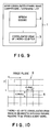
- segmental unit of a page is square in order to simplify explanation.
- an image plane is segmented into square page ranges 6 with a side of X pixels, and each of the squares is stored so as to correspond to a page of the DRAM.
- a square image 7 with a side of Y pixels is read out on the basis of the position from the origin having optional coordinates (random).
- the image 7 extends over nine lattices (segmented regions). Therefore, only the issuance of the command consumes a power nine time as many as the unit power consumption.
- the coordinates of the origin are random ones, an expected value of the number of lattices over which the image extends is derived as follows.
- the expected value VE of the number of lattices over which the image extends is calculated by the following expression.
- VE ((Z-1) 2 (N+1) 2 + 2(Z-1)(X-Z+1)N(N+1) + (X-Z+1) 2 N 2 ⁇ / X 2
- the basic image is a block of 8 x 8 pixels or a macro block of 16 x 16 pixels, so that Y is 8 or 16.
- X capable of extremely reducing the power consumption is derived (N and Z can be calculated from X).
- FIG. 7 a characteristic diagram shown in FIG. 7 is obtained.
- the power consumption is effectively reduced when X is in the range of from 8 to 32 about the number of pixels of 16.
- This is a page size which is in the range of from 64 bytes to 512 byte per page. It is considered that the page size of this range is effective in the decrease of power consumption when the image of the square region of "16 pixels x 16 pixels" is read.
- the second preferred embodiment of a memory-consolidated image-processing LSI will be described below.
- the page size has been defined, whereas in this second preferred embodiment, a word size is defined.
- the memory-consolidated image processing LSI in the second preferred embodiment is different from that in the first preferred embodiment.
- the word is an access unit in the second stage of the two-stage accesses.
- the memory consolidated image processing LSI 1 comprises an MPEG-4 CODEC 2, and a DRAM 3 having a word size of 16 bytes.
- the size of data stored in the DRAM 3 is set to be 16 bytes per one word although it is set to be 256 byte per one page in the first preferred embodiment.
- the size of one word is 16 bytes as an example, but it may be in the range of from 8 bytes to 64 bytes, preferably the number of bytes which is a power of "8".
- the CODEC 9 may be adapted to other standards, such as MPEG-1, MPEG-2 and H.263, or may be another kind of dynamic image compressing or expanding CODEC for carrying out a motion compensation every block.
- the CODEC may have another construction if it is an image processing circuit for accessing a substantially square image with a side of 8 pixels or 16 pixels from random coordinates.
- the consolidated DRAM 3 of the memory consolidated image processing LSI in the second preferred embodiment shown in FIG. 9 is segmented into square areas, each of which has the same capacity as that of the word, or rectangular areas with sizes 1 : 2 length, for storing data in different words.
- regions 8 having a size of "4 pixels x 4 pixels” are stored in x and y directions with respect to the image plane 5. Therefore, in FIG. 10, the segmented images of square regions, each of which has a size of "4 pixels x 4 pixels", are word ranges 8, so that the word has a size of 16 bytes.
- the memory consolidated image processing LSI in the second preferred embodiment has been designed to store data of 16 bytes as a word in the word range 8 of "4 pixels x 4 pixels" as shown in FIG. 10, the present invention should not be limited thereto.
- the image plane 5 may be segmented into rectangular word ranges 8 corresponding to regions of "8 pixels x 2 pixels" on a two-dimensional plane of the image plane 5 stored in the consolidated DRAM 3.
- data stored in the consolidated DRAM 3 has a word size of 16 bytes, and the image is segmented into rectangular regions of "8 pixels x 2 pixels" to store data every word.
- the size of a page may be set so as to increase the possibility of statistically minimizing the power consumption when a substantially square image with a side of about 8 pixels to 16 pixels, which is often used for an image processing such as a motion compensation, is accessed from the DRAM by the word on the basis of random coordinates.
- the word is an access unit when the DRAM is accessed.
- it is required to issue an appropriate command for the DRAM.
- the image is segmented into squares.
- an image plane may be segmented into square ranges with a side of X pixels. It is assumed that each of the squares is stored so as to correspond to a word of the DRAM. It is assumed that from this plane, a square image with side Y pixels long is read out on the basis of the position from the origin having optional coordinates. Similar to the setting of the region of a page in which a page access is carried out, Z and N can be defined.
- the expected value VE of the number of lattices over which the image extends is derived by the following expression.
- VE ⁇ (Z-1) 2 (N+1) 2 + 2(Z-1)(X-Z+1)N(N+1) + (X-Z+1) 2 N 2 ⁇ / X 2
- These characteristic diagrams show normalized power consumption plotted with respect to the length X of a side of an image corresponding to a page. It can be seen that the normalized power consumption has substantially minimum values when the length X is in the range of 2 pixels or 4 pixels to 8 pixels. This means that the possibility that the use of a DRAM having a word size of 8 bytes to 64 bytes is advantageous to save power consumption is high. Also when an image having a similar shape or area is stored or accessed, the same effect can be obtained in such a range of page construction.
- FIG. 12 shows a case where a partial image of "16 pixels x 16 pixels" is accessed at random
- FIG. 13 shows a case where a partial image of "8 pixels x 8 pixels" is accessed at random.
- the optimum shape of the partial image stored in the page region is square.
- a rectangle of "1 : 2" or "1 : 4" is preferred next to the first case as the shape of the partial image which is easy to be collectively stored.
- the memory consolidated image processing LSI in the third preferred embodiment has the same construction as the LSI 1 in the first and second preferred embodiments, and comprises an MPEG-4 CODEC 2 and a consolidated DRAM 3.
- the construction of the consolidated DRAM 3 is a combination of data storage forms of the consolidated DRAMs in the first and second preferred embodiments.
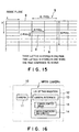
- the third preferred embodiment is different from the first and second preferred embodiments. That is, in FIG. 14, the consolidated DRAM 3 is set so as to have a size of 16 bytes per word and a capacity of 256 bytes per page.
- FIG. 15 shows an example wherein data is stored in the DRAM 3 having a page size of 256 bytes and a word size of 16 bytes.
- 16 word ranges 8 of 16 bytes are assembled to form a page range 6 for one page, and the page range 6 has a size of "16 pixels x 16 pixels" of 256 bytes.
- image data for one frame is intended to be accessed by a motion compensation processing or the like
- the image data for one page of 16 pixels in x directions and 16 pixels in y directions is first accessed, and then, the image data for one word of 8 pixels in x directions and 2 pixels in y directions is accessed, so that it is possible to efficiently store and read DRAM stored image data having the optimum size, together with page data and word data, at a low power consumption.
- the memory part has comprised the dynamic random access memory (DRAM) in the above described memory consolidated image processing LSIs in the first through third preferred embodiments, the present invention should not be limited thereto.
- the memory consolidated image processing LSI has page and word regions as a memory region and has the above described construction for carrying out two-stage accesses that a word access is carried out after a page access is carried out
- the memory part may comprises a ferroelectric random access memory (FRAM) or a magnetoresistance random access memory (MRAM).
- FRAM ferroelectric random access memory
- MRAM magnetoresistance random access memory
- FIGS. 16 through 18 While the internal construction of the consolidated DRAM 3 constituting the LSI 1 has been described in the first through third preferred embodiment, the fourth through sixth preferred embodiments of the present invention to which a memory consolidated image processing LSI according to the present invention is applied will be described referring to FIGS. 16 through 18.
- FIG. 16 is a block diagram showing the fourth preferred embodiment of a memory consolidated image processing LSI according to the present invention, which is applied to an MPEG camera as an example of an image processing system, particularly a portable electronic apparatus capable of being driven by a battery.
- an MPEG camera 10 comprises a camera 11 and a memory consolidated image processing LSI 12.
- the LSI 12 comprises a camera interface 13, an MPEG compressing circuit 14 and a consolidated DRAM 15 with the construction in any one of the first through third preferred embodiments.
- the camera interface 13, the MPEG compressing circuit 14 and the consolidated DRAM 15 constitute a large scale integrated circuit.
- the basic construction of the memory consolidated image processing LSI in the fourth preferred embodiment is the same as those of the memory consolidated image processing LSIs in the first through third preferred embodiment, except that the camera interface 13 is added. Furthermore, image data to be outputted from the camera are not outputted while the image size is segmented into lattice-like parts. In such a case, after the image data are temporarily stored in the memory, the rearrangement of images stored so that the image data segmented into lattice-like parts correspond to a page region of the memory may be carried out.
- the memory consolidated image processing LSI 12 further comprises the camera interface 13 in addition to the MPEG compressing circuit 14 and the consolidated DRAM 15. Therefore, if the LSI 12 is applied to, e.g., an image control part of the camera 11 with substantially the same construction as that of a conventional camera, there is a peculiar advantage in that it is possible to easily provide the MPEG camera 10.
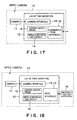
- FIG. 17 is a block diagram showing the construction of the fifth preferred embodiment of an MPEG camera according to the present invention.
- an MPEG camera 10 comprises a camera 11 and a memory consolidated image processing LSI 12.
- LSI 12 a camera interface 13
- MPEG compressing circuit 14 a consolidated DRAM 15
- a communication interface 16 for transmitting an image picked up by the MPEG camera to the outside are mounted on the same chip.
- the MPEG camera 10 in the fifth preferred embodiment there is a peculiar advantage in that the image picked up by the camera can be transmitted to the outside via the communication interface 16.
- the communication interface 16 has been mounted on the same chip as that for the memory consolidated image processing LSI 12, the present invention should not be limited thereto.
- the communication interface 16 may be formed as a separate chip to be connected to the MPEG compressing circuit 14 via data transmitting/-receiving wiring.
- an MPEG compression signal received via the communication interface may be expanded by an MPEG expanding circuit (not shown) to display an image on a monitor (not shown). Also to such an image expanding processing, the memory access construction of the present invention can be applied.
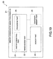
- FIG. 18 is a block diagram showing the construction of the sixth preferred embodiment of an MPEG camera according to the present invention.
- an MPEG camera 10 comprises a camera 11, a memory consolidated image processing LSI 12, and a recording unit 18.
- the LSI 12 comprises a camera interface 3, an MPEG compressing circuit 14, a consolidated DRAM 15, and a data interface 17 for transmitting and receiving image data to and from the recording unit 18.
- the picked-up image can be recorded in the recording unit 18, which is provided in the MPEG camera 10, by means of the data interface 17 mounted on the same chip, so that the functions of the MPEG compressing circuit and the consolidated DRAM, which are the features of the present invention, can also be given to the recorded image.
- the data interface 17 may comprise a discrete circuit in the sixth preferred embodiment.
- the memory consolidated image processing LSI according to the present invention can be applied to the MPEG camera in any one of the fourth through sixth preferred embodiment, and the present invention can reduce the power consumption when page and word data are accessed with respect to the consolidated DRAM, so that there is an excellent advantage in that it is possible to easily provide an excellent portable MPEG camera.
- the application of a memory consolidated image processing LSI according to the present invention should not be limited to the MPEG camera, but the invention can be applied to all of image processing systems including a portable TV telephone.
- the memories to which the present invention is applied should not be limited to DRAMS, but the invention may be applied to FeRAMs and MRAMs if the memories are designed to carry out two-stage accesses as described above.
- the first through third preferred embodiments of a memory consolidated image processing LSI according to the present invention may be mounted on the seventh preferred embodiment of an image processing system according to the present invention which will be described below.
- an image processing system 20 in this seventh preferred embodiment has the image compressing and/or expanding function of compressing and/or expanding image information.
- the image processing system 20 comprises: a memory part 23 having a plurality of lattice-like page ranges for storing image data for the page ranges, which are formed by segmenting an image plane corresponding to a display screen and each of which has sides a power of 2 long, and a plurality of word regions for storing image data for a plurality of word ranges which are formed by segmenting each of the page ranges, the word regions being assembled to constitute the page region; and an image access part 22 for accessing the word ranges after accessing the page ranges by a pre-charge in order to access the memory part.
- each of the page ranges and each of the word range in the memory part 23 of the memory consolidated image processing LSI 21 may a desired page range and a desired word range, which allow desired image data to be accessed at the minimum power consumption by the minimum number of pre-charges and the minimum number of charges.
- the image processing system 20 in the seventh preferred embodiment may further comprise: a raster converting part 24 for raster-converting the image information; and a processing part 25 for converting the image data, which has been converted by the raster converting part 24, into data corresponding to the desired page and word ranges, wherein the memory consolidated image processing LSI 21 stores the image data for the desired page and word ranges, which has been converted by the processing part 25, in the page and word regions of the memory part, and the image access part 22 word-accesses the desired word region after being pre-charged in the desired page region of the memory part.
- the image processing system in the seventh preferred embodiment may further comprise: a raster converting part 24 for raster-converting the image information; a temporary memory part 26 for temporarily storing the image data which has been converted by the raster converting part 24; and a processing part 25 for converting the image data, which has been stored in the temporary memory part 25, into data corresponding to the desired page and word ranges, wherein the memory consolidated image processing LSI stores the desired page and word ranges, which have been converted by the processing part, in the page and word regions of the memory part, and the image access part 22 accesses the desired word region after being pre-charged in the desired page region of the memory part.
- the image processing system in the seventh preferred embodiment may further comprise an MPEG processing part for compression-coding the image data using an MPEG coding system, wherein the memory consolidated image processing LSI stores the desired page and word ranges for the image data, which has been converted by the MPEG processing part, in the memory part, and the image access part word-accesses the desired word region after being pre-charged in the desired page range of the memory part.
- the image access part may be a circuit for processing a bit stream based on a dynamic image compressing standard, such as MPEG-4, MPEG-2, MPEG-1 or H.263, and the memory part may be a memory having the page region corresponding to the page range serving as a unit for the preparation for reading, the size of the page range on the image plane being preferably in the range of from 64 pixels to 512 pixels.
- a dynamic image compressing standard such as MPEG-4, MPEG-2, MPEG-1 or H.263
- the memory part may be a memory having the page region corresponding to the page range serving as a unit for the preparation for reading, the size of the page range on the image plane being preferably in the range of from 64 pixels to 512 pixels.
- the image access part may be a circuit for processing a bit stream based on a dynamic image compressing standard, such as MPEG-4, MPEG-2, MPEG-1 or H.263, and the memory part may be a memory having the page region corresponding to the page range serving as a unit for the preparation for reading, the size of the page range on the image plane being preferably in the range of from 512 pixels to 1024 pixels.
- a dynamic image compressing standard such as MPEG-4, MPEG-2, MPEG-1 or H.263
- the memory part may be a memory having the page region corresponding to the page range serving as a unit for the preparation for reading, the size of the page range on the image plane being preferably in the range of from 512 pixels to 1024 pixels.
- the image access part may be a circuit for processing a bit stream based on a dynamic image compressing standard, such as MPEG-4, MPEG-2, MPEG-1 or H.263, and the memory part may be a memory having the word region corresponding to the word range serving as a unit corresponding to a data bus, the size of the word range on the image plane being preferably in the range of from 8 pixels to 64 pixels.
- a dynamic image compressing standard such as MPEG-4, MPEG-2, MPEG-1 or H.263
- the memory part may be a memory having the word region corresponding to the word range serving as a unit corresponding to a data bus, the size of the word range on the image plane being preferably in the range of from 8 pixels to 64 pixels.
- the image access part may be a circuit for processing a bit stream based on a dynamic image compressing standard, such as MPEG-4, MPEG-2, MPEG-1 or H.263, and the memory part may be a memory having the word region corresponding to the word range serving as a unit corresponding to a data bus, the size of the word range on the image plane being preferably in the range of from 64 pixels to 256 pixels.
- a dynamic image compressing standard such as MPEG-4, MPEG-2, MPEG-1 or H.263
- the memory part may be a memory having the word region corresponding to the word range serving as a unit corresponding to a data bus, the size of the word range on the image plane being preferably in the range of from 64 pixels to 256 pixels.
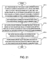
- the eighth preferred embodiment of an image data processing method is a method for processing image data stored in a memory consolidated image processing LSI 21 shown in FIG. 19, which comprises a memory part 23 for storing predetermined image data and having page regions each storing page ranges so that an image plane corresponding to a display screen is segmented into lattice-like ranges each of which has sides a power of 2 long, and a word regions each storing word ranges which are formed by segmenting the page range on the image plane, and an access part 22 for accessing to the memory part in the manner that a multiplied value of a power consumption per one of pre-charges in a power consumption model of a memory by an average number of the pre-charges is a substantially minimum value and that a multiplied value of a power consumption per one of word accesses in a power consumption model of a memory by an average number of the word accesses is a substantially minimum value.
- the method comprises: a step ST1 of accessing in a first stage by pre-charging to the page region of the memory part in which desired data are stored; a step ST2 of accessing in a second stage by ward accessing to the word regions of the memory part in which desired data are stored; a step ST3 of reading out the desired data from the memory part; and a step ST 4 of performing predetermined image processing to image data which are read in the manner that a multiplied value of a power consumption per one of pre-charges in a power consumption model of a memory by an average number of the pre-charges is a substantially minimum value, or a multiplied value of a power consumption per one of word accesses in a power consumption model of a memory by an average number of the word accesses is a substantially minimum value.
- the page region in the memory part is set to have a size so that the multiplied value of the power consumption per one of the pre-charges in a power consumption model of a memory by an average number of pre-charges is the substantially minimum value.
- the word region in the memory part is set to have a size so that the multiplied value of a power consumption per one of word accesses in a power consumption model of a memory by an average number of the word accesses is the substantially minimum value.
- the page region in the memory part is set to have a size so that the multiplied value of the power consumption per one of the pre-charges in a power consumption model of a memory by an average number of pre-charges is the substantially minimum value
- the word region in the memory part is set to have a size so that the multiplied value of a power consumption per one of word accesses in a power consumption model of a memory by an average number of the word accesses is the substantially minimum value.
- the image processing performed in step ST4 includes various of processing such as a compression, decompression, motion vector compensation and the like of moving picture data.
- the method for designing a memory consolidated image processing LSI comprises a memory part for storing predetermined image data, and an access part for accessing the image data stored in the memory part by using two-stage accesses.
- the designing method comprises: a step ST11 of setting a plurality of page ranges so that an image plane corresponding to a display screen is segmented into lattice-like ranges, each of which has sides a power of 2 long, and so that the multiplied value of the power consumption per one of the pre-charges in a power consumption model of a memory by an average number of pre-charges is the substantially minimum value; a step ST12 of setting a page region capable of storing the image data for a page range on the image plane in the memory part; a step ST13 of setting a plurality of word ranges which are formed by segmenting the page range on the image plane so that the multiplied value of a power consumption per one of word accesses in a power consumption model of a memory by an average number of the word accesses is the substantially minimum value; a step ST14 of setting a word region capable of storing the word ranges on the image plane in the page region in the memory part; and a step ST15 of storing the image data
- the image of the optimum range on a screen which is easy to process the image of the page and word memory regions of the memory for carrying out two-stage accesses for storing the image plane, is divided into page range images and/or word range images to be stored. Therefore, there is an advantage in that it is possible to efficiently carry out reading when accessing a page storage image of a large power consumption, so that it is possible to reduce the power consumption which is required for reading image data from the consolidated DRAM.
Landscapes
- Engineering & Computer Science (AREA)
- Multimedia (AREA)
- Signal Processing (AREA)
- Physics & Mathematics (AREA)
- Computer Hardware Design (AREA)
- General Physics & Mathematics (AREA)
- Theoretical Computer Science (AREA)
- Dram (AREA)
- Image Input (AREA)
- Image Processing (AREA)
- Compression Of Band Width Or Redundancy In Fax (AREA)
Applications Claiming Priority (2)
| Application Number | Priority Date | Filing Date | Title |
|---|---|---|---|
| JP2000027911 | 2000-02-04 | ||
| JP2000027911A JP4162348B2 (ja) | 2000-02-04 | 2000-02-04 | メモリ混載画像処理用lsiおよび画像処理装置 |
Publications (2)
| Publication Number | Publication Date |
|---|---|
| EP1122713A2 true EP1122713A2 (fr) | 2001-08-08 |
| EP1122713A3 EP1122713A3 (fr) | 2007-03-07 |
Family
ID=18553416
Family Applications (1)
| Application Number | Title | Priority Date | Filing Date |
|---|---|---|---|
| EP20010102174 Withdrawn EP1122713A3 (fr) | 2000-02-04 | 2001-02-02 | Circuit LSI de traitement d'image comportant une mémoire, système de traitement d'image comportant ce circuit et méthode d'accès à une image utilisant ce circuit |
Country Status (4)
| Country | Link |
|---|---|
| US (1) | US6750871B2 (fr) |
| EP (1) | EP1122713A3 (fr) |
| JP (1) | JP4162348B2 (fr) |
| KR (1) | KR100419271B1 (fr) |
Cited By (1)
| Publication number | Priority date | Publication date | Assignee | Title |
|---|---|---|---|---|
| WO2003045046A2 (fr) * | 2001-11-21 | 2003-05-30 | Electronics And Telecommunications Research Institute | Systeme et procede de traitement video stereoscopique/multivue tridimensionnel |
Families Citing this family (2)
| Publication number | Priority date | Publication date | Assignee | Title |
|---|---|---|---|---|
| US7889206B2 (en) * | 2003-06-16 | 2011-02-15 | Broadcom Corporation | Direct memory accessing for fetching macroblocks |
| US9600744B2 (en) | 2012-04-24 | 2017-03-21 | Stmicroelectronics S.R.L. | Adaptive interest rate control for visual search |
Citations (3)
| Publication number | Priority date | Publication date | Assignee | Title |
|---|---|---|---|---|
| EP0371488A2 (fr) * | 1988-11-29 | 1990-06-06 | Matsushita Electric Industrial Co., Ltd. | Mémoire à accès aléatoire dynamique pour vidéo |
| EP0649100A2 (fr) * | 1993-10-15 | 1995-04-19 | Hitachi, Ltd. | Système de traitement de données et système de traitement d'images |
| US5706480A (en) * | 1995-10-04 | 1998-01-06 | Lg Semicon Co., Ltd. | Memory device and method for processing digital video signal |
Family Cites Families (5)
| Publication number | Priority date | Publication date | Assignee | Title |
|---|---|---|---|---|
| JPS60195589A (ja) * | 1984-03-19 | 1985-10-04 | オリンパス光学工業株式会社 | 画像表示装置 |
| JP3214132B2 (ja) * | 1993-03-01 | 2001-10-02 | 三菱電機株式会社 | メモリセルアレイ半導体集積回路装置 |
| JPH08123953A (ja) * | 1994-10-21 | 1996-05-17 | Mitsubishi Electric Corp | 画像処理装置 |
| JP3664777B2 (ja) * | 1995-08-18 | 2005-06-29 | 株式会社ルネサステクノロジ | 半導体記憶装置 |
| JPH10134566A (ja) * | 1996-10-31 | 1998-05-22 | Mitsubishi Electric Corp | 記憶機能を有する半導体装置及びそのデータ読み出し方法 |
-
2000
- 2000-02-04 JP JP2000027911A patent/JP4162348B2/ja not_active Expired - Fee Related
-
2001
- 2001-02-02 EP EP20010102174 patent/EP1122713A3/fr not_active Withdrawn
- 2001-02-02 US US09/773,625 patent/US6750871B2/en not_active Expired - Fee Related
- 2001-02-03 KR KR10-2001-0005265A patent/KR100419271B1/ko not_active IP Right Cessation
Patent Citations (3)
| Publication number | Priority date | Publication date | Assignee | Title |
|---|---|---|---|---|
| EP0371488A2 (fr) * | 1988-11-29 | 1990-06-06 | Matsushita Electric Industrial Co., Ltd. | Mémoire à accès aléatoire dynamique pour vidéo |
| EP0649100A2 (fr) * | 1993-10-15 | 1995-04-19 | Hitachi, Ltd. | Système de traitement de données et système de traitement d'images |
| US5706480A (en) * | 1995-10-04 | 1998-01-06 | Lg Semicon Co., Ltd. | Memory device and method for processing digital video signal |
Cited By (4)
| Publication number | Priority date | Publication date | Assignee | Title |
|---|---|---|---|---|
| WO2003045046A2 (fr) * | 2001-11-21 | 2003-05-30 | Electronics And Telecommunications Research Institute | Systeme et procede de traitement video stereoscopique/multivue tridimensionnel |
| WO2003045046A3 (fr) * | 2001-11-21 | 2003-10-09 | Korea Electronics Telecomm | Systeme et procede de traitement video stereoscopique/multivue tridimensionnel |
| CN100428804C (zh) * | 2001-11-21 | 2008-10-22 | 韩国电子通信研究院 | 3d立体/多视图视频处理系统及其方法 |
| US8111758B2 (en) | 2001-11-21 | 2012-02-07 | Electronics And Telecommunications Research Institute | 3D stereoscopic/multiview video processing system and its method |
Also Published As
| Publication number | Publication date |
|---|---|
| EP1122713A3 (fr) | 2007-03-07 |
| KR20010078328A (ko) | 2001-08-20 |
| JP2001216503A (ja) | 2001-08-10 |
| US6750871B2 (en) | 2004-06-15 |
| JP4162348B2 (ja) | 2008-10-08 |
| KR100419271B1 (ko) | 2004-02-18 |
| US20010013081A1 (en) | 2001-08-09 |
Similar Documents
| Publication | Publication Date | Title |
|---|---|---|
| US8531546B2 (en) | Image processing apparatus having a buffer memory for image data storage | |
| US8866646B2 (en) | Memory compression technique with low latency per pixel | |
| US8648931B2 (en) | Systems and methods for capturing images of objects | |
| US8295361B2 (en) | Video compression circuit and method thereof | |
| US6633608B1 (en) | Method and apparatus for adapting memory resource utilization in an information stream decoder | |
| CN101896941A (zh) | 统一的压缩/解压缩图形体系结构 | |
| US20050134907A1 (en) | Image information processing system and image information processing method | |
| US7545416B2 (en) | Image processing device and camera including CPU which determines whether processing performed using external memory | |
| KR100912560B1 (ko) | 텔레비젼 수상 장치 | |
| US6750871B2 (en) | Memory consolidated image processing LSI, image processing system with same, and image accessing method using same | |
| US6473527B1 (en) | Module and method for interfacing analog/digital converting means and JPEG compression means | |
| US6249617B1 (en) | Video encounter having an integrated scaling mechanism | |
| US7787701B2 (en) | Image processing apparatus and apparatus connected to image processing apparatus | |
| EP3816925A1 (fr) | Procédé et système d'accès coordonné pour mémoire externe, et architecture d'accès coordonné | |
| KR100353894B1 (ko) | 제이펙 화상 데이터 버퍼링을 위한 메모리 구조 및 주소어드레스 방법 | |
| US7154559B2 (en) | Video apparatus, notably video decoder, and process for memory control in such an apparatus | |
| US6907078B2 (en) | Method for storing compressed MPEG image with low power consumption and frame buffer structure used in the same | |
| US20040213467A1 (en) | Image processing apparatus | |
| US6297831B1 (en) | Image generator using display memory | |
| KR0172577B1 (ko) | 스틸카메라의 메모리제어방법 | |
| TW577229B (en) | Module and method for graphics display | |
| US20070195168A1 (en) | Web camera | |
| US20040183948A1 (en) | Real time smart image scaling for video input | |
| EP1239671B1 (fr) | Appareil vidéo, en particulier décodeur vidéo, et procédé de contrôle de mémoire d'un tel appareil | |
| JP2004235767A (ja) | 携帯端末機器 |
Legal Events
| Date | Code | Title | Description |
|---|---|---|---|
| PUAI | Public reference made under article 153(3) epc to a published international application that has entered the european phase |
Free format text: ORIGINAL CODE: 0009012 |
|
| 17P | Request for examination filed |
Effective date: 20010202 |
|
| AK | Designated contracting states |
Kind code of ref document: A2 Designated state(s): AT BE CH CY DE DK ES FI FR GB GR IE IT LI LU MC NL PT SE TR |
|
| AX | Request for extension of the european patent |
Free format text: AL;LT;LV;MK;RO;SI |
|
| PUAL | Search report despatched |
Free format text: ORIGINAL CODE: 0009013 |
|
| AK | Designated contracting states |
Kind code of ref document: A3 Designated state(s): AT BE CH CY DE DK ES FI FR GB GR IE IT LI LU MC NL PT SE TR |
|
| AX | Request for extension of the european patent |
Extension state: AL LT LV MK RO SI |
|
| 17Q | First examination report despatched |
Effective date: 20070620 |
|
| AKX | Designation fees paid |
Designated state(s): DE FR |
|
| STAA | Information on the status of an ep patent application or granted ep patent |
Free format text: STATUS: THE APPLICATION IS DEEMED TO BE WITHDRAWN |
|
| 18D | Application deemed to be withdrawn |
Effective date: 20100901 |