EP1120926B1 - Article comprising a single-stage all-pass optical filter - Google Patents
Article comprising a single-stage all-pass optical filter Download PDFInfo
- Publication number
- EP1120926B1 EP1120926B1 EP01300309A EP01300309A EP1120926B1 EP 1120926 B1 EP1120926 B1 EP 1120926B1 EP 01300309 A EP01300309 A EP 01300309A EP 01300309 A EP01300309 A EP 01300309A EP 1120926 B1 EP1120926 B1 EP 1120926B1
- Authority
- EP
- European Patent Office
- Prior art keywords
- repetition rate
- filter
- optical filter
- optical
- pulse train
- Prior art date
- Legal status (The legal status is an assumption and is not a legal conclusion. Google has not performed a legal analysis and makes no representation as to the accuracy of the status listed.)
- Expired - Lifetime
Links
- 230000003287 optical effect Effects 0.000 title claims description 121
- 238000004891 communication Methods 0.000 claims description 14
- 230000001419 dependent effect Effects 0.000 claims description 11
- 238000001228 spectrum Methods 0.000 claims description 9
- 230000003595 spectral effect Effects 0.000 claims description 4
- 238000010438 heat treatment Methods 0.000 claims description 3
- 238000001914 filtration Methods 0.000 claims description 2
- 238000000034 method Methods 0.000 claims 7
- 230000005540 biological transmission Effects 0.000 claims 2
- 230000008878 coupling Effects 0.000 description 9
- 238000010168 coupling process Methods 0.000 description 9
- 238000005859 coupling reaction Methods 0.000 description 9
- 230000003111 delayed effect Effects 0.000 description 7
- 239000000835 fiber Substances 0.000 description 5
- 230000001360 synchronised effect Effects 0.000 description 5
- 239000013307 optical fiber Substances 0.000 description 4
- 239000006185 dispersion Substances 0.000 description 3
- 230000000694 effects Effects 0.000 description 3
- 230000005693 optoelectronics Effects 0.000 description 2
- 230000009286 beneficial effect Effects 0.000 description 1
- 230000001934 delay Effects 0.000 description 1
- 238000004519 manufacturing process Methods 0.000 description 1
- 238000012986 modification Methods 0.000 description 1
- 230000004048 modification Effects 0.000 description 1
- 230000004044 response Effects 0.000 description 1
Images


Classifications
-
- H—ELECTRICITY
- H04—ELECTRIC COMMUNICATION TECHNIQUE
- H04J—MULTIPLEX COMMUNICATION
- H04J14/00—Optical multiplex systems
- H04J14/08—Time-division multiplex systems
-
- G—PHYSICS
- G02—OPTICS
- G02B—OPTICAL ELEMENTS, SYSTEMS OR APPARATUS
- G02B5/00—Optical elements other than lenses
- G02B5/20—Filters
-
- H—ELECTRICITY
- H04—ELECTRIC COMMUNICATION TECHNIQUE
- H04B—TRANSMISSION
- H04B10/00—Transmission systems employing electromagnetic waves other than radio-waves, e.g. infrared, visible or ultraviolet light, or employing corpuscular radiation, e.g. quantum communication
- H04B10/50—Transmitters
- H04B10/501—Structural aspects
- H04B10/503—Laser transmitters
- H04B10/504—Laser transmitters using direct modulation
-
- H—ELECTRICITY
- H04—ELECTRIC COMMUNICATION TECHNIQUE
- H04B—TRANSMISSION
- H04B10/00—Transmission systems employing electromagnetic waves other than radio-waves, e.g. infrared, visible or ultraviolet light, or employing corpuscular radiation, e.g. quantum communication
- H04B10/50—Transmitters
- H04B10/508—Pulse generation, e.g. generation of solitons
Definitions
- the present invention relates to optical communications systems and more particularly, to an article comprising a single-stage all-pass optical filter.
- Optical communications systems typically include a variety of devices (e.g., light sources, photodetectors, switches, optical fibers, amplifiers, filters, and so forth). Optical communications systems are useful for transmitting optical signals over long distances at high speeds.
- An optical signal which comprises a series of light pulses, is transmitted from a light source such as a laser to an optical fiber and ultimately to a detector.
- Amplifiers and filters may be used to propagate the light pulses along the length of the fiber from the light source to the detector.
- Today, the bulk of long-distance communication traffic is carried by optical fibers. As use of optical fibers becomes more widespread and infiltrates the consumer marketplace, demand is increasing for efficient, high-speed, integrated opto-electronic devices.
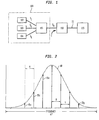
- FIG. 1 reflects a schematic representation of an OTDM system, comprising a time-division multiplexer (TDM) 100 which includes a plurality of low-speed transmitters 102, 103, 104 and a multiplexer 105, an optical switch or demultiplexer 110, and a receiver 115, connected by trunk fiber 11.
- TDM time-division multiplexer
- Each of the transmitters sends low speed signals (s L ) to the multiplexer 105 which then outputs a high speed signal (s H ) to the switch 110.
- the switch selectively drops pulses from the high-speed signal to produce low-speed output signals (s o ) sent to receiver 115.
- the signals may be sent at high-speed over the length of the fiber between the multiplexer 105 and the switch 110, and then interpreted at low speed to determine the information sent from each one of the transmitters.
- FIG. 2 is a graphical illustration showing the spectrum of an unmodulated pulse train.
- an optical pulse 10 typically comprises a packet of waves 15a, 15b, 15c ...
- Each wave has a certain amplitude and frequency within the bandwidth ⁇ , e.g ., each wave within the packet is characterized by a different frequency and amplitude and travels at a different speed. Challenges are involved in achieving a constant time delay for each ofthe frequencies over the entire bandwidth ⁇ . If certain frequencies of the pulse train (e.g. 15a, 15b), are not delayed or are given a different period of delay than other frequencies (e.g ., 15c, 15d), the delayed signal will not correspond in phase with the original pulse train.
- certain frequencies of the pulse train e.g. 15a, 15b
- other frequencies e.g ., 15c, 15d
- All-pass filters have been known in the field of electronics for equalizing phase and reducing distortion. Structures for fabricating all-pass filters for electronic devices are known in the field and described in the literature. See, e.g ., U.S. Pat. No. 5,258,716 to Kondo et al ., " All-Pass Filter.” All-pass filters provide advantages over other types of filters as they affect only the phase of a signal, rather than its amplitude. A configuration for an all-pass filter for use with optical devices is described in EP-A-0 997 751; filed by Kazarinov et al.
- an optical signal transmitted through a fiber may be distorted or broadened with time over the length of the fiber. This broadening is undesirable as it may create noise, i . e ., interference between sequential optical pulses.
- the Kazarinov et al. application describes an all-pass optical filter designed to eliminate such distortions. Additionally, it was disclosed therein that the all-pass optical filter could be useful in delaying an optical pulse in time.
- the all-pass optical filter of the Kazarinov et al. application applies a frequency-dependent time delay to each frequency of the optical pulse.
- the Kazarinov et al. application describes single-stage and multiple-stage all-pass optical filters.
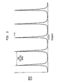
- a schematic representation of one embodiment a single-stage all-pass optical filter according to the Kazarinov et al. application is illustrated in FIG. 3.
- the filter comprises an input port for an input optical pulse 120, an output port 150, a splitter/combiner 143, and a feedback path 145 wherein the feedback path advantageously comprises at least one ring resonator.
- FIG. 3 shows a single-stage filter (e.g ., a single resonator ring)
- the Kazarinov et al. application discloses that best results are achieved when multiple stages (multiple resonator rings) are used. Indeed, the Kazarinov et al.
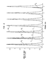
- FIG. 4 is a graph of the group delay in units of time as a function of frequency for a four-stage all pass optical filter as applied to an arbitrary broadband signal.
- a maximum and fairly constant delay of 16 au is achieved over the normalized frequency range of 0.4 to 0.6.
- a single all-pass optical filter would achieve a constant delay over a much smaller frequency range ( ⁇ 05) and thus would be ineffective in delaying a pulse train having a large bandwidth ( ⁇ ).
- many all-pass stages would increase the bandwidth ( ⁇ ) of the maximum delay period and also lessen the ripple effect.
- a ripple effect is created over the delay period in that four separate summits appear at the maximum height of the delay peak.
- the four-stage all-pass optical filter used to produce the delay peak shown in FIG. 4 would include the use of eight heaters, each of which would be need to be periodically adjusted depending on the optical signal and desired phase response.
- the invention embraces an article comprising a single-stage all-pass optical filter.
- the all-pass optical filter includes an input port for receiving an input optical pulse having a regular repetition rate; an output port; a splitter/combiner; and one feedback path.
- the all-pass optical filter is configured to apply a plurality of frequency-dependent time delay periods to the input optical pulse so that the filter is characterized by a time-delay spectrum having a plurality of delay peaks.
- the free-spectral range (FSR) of the filter i.e ., the spacing between the delay peaks, is matched to the regular repetition rate of the input optical pulse.
- the FSR being equal to the repetition rate or offset from the repetition rate to a sufficiently small degree that each frequency of the pulse train will fall within the bandwidth of one of the plurality of delay peaks.
- at least one heater is disposed on the feedback path for use in tuning the time-delay spectrum of the filter.
- the article including the single-stage all-pass optical filter may comprise an assembly for use in a communications system including an OTDM device or a pulsed laser.
- the invention comprises a single stage all-pass optical filter that can be used to generate a large tunable delay for a regular unmodulated pulse train.
- a single-stage all-pass optical filter can be used to generate a large tunable delay for the signal.
- a single-stage all-pass optical filter can be effective in correcting certain dispersion such as the linear chirp of a pulsed laser.
- FSR free spectral range
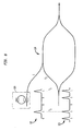
- This all-pass optical filter 130 includes a feedback path 145, an input port 140 for receiving optical pulse 120, an output port 150, and a splitter/combiner 143 for coupling portions of the input optical pulse into and away from the feedback path 145.
- the feedback path of the all-pass optical filter may have a ring resonator structure, as schematically shown. According to the invention, only one ring resonator structure is used and yet a large tunable delay or chirp correction is achieved, thus providing advantages over the filter of the Kazarinov et al. application.
- a heating element 185 is advantageously disposed on the ring.
- the optical pulse 120 that enters the all-pass optical filter comprises a regular unmodulated pulse train.
- regular herein, it is meant that the pulse train has a regular repetition rate as illustrated in FIG. 2 and described above, i.e ., each of the frequencies of the pulse train differ from another ( i.e ., adjacent) frequency of the pulse train by the same amount which is represented in FIG. 2 as value "R.”
- the output port 150 At each pass of the optical pulse in the feedback path 145, some portion thereof is provided through the splitter/combiner 143 to the output port 150, which incrementally reduces the portion of the optical pulse introduced into the feedback path 145, in effect removing it therefrom.
- the length of the feedback path 145 is typically shorter than the optical pulse length.
- the input optical pulse 120 repeatedly circulates along the feedback path 145, it interferes with itself. That is, leading edge portions of the optical signal circulating in the feedback path interfere with trailing edge portions of the optical signal being input thereto. Interference between the leading and trailing edges of the optical pulse applies a frequency-dependent time delay to the frequencies of the optical pulse. After the frequency-dependent time delays are applied to each frequency of the optical pulse, the pulse is output from the filter through the output port 150.
- the time delay applied by the filter can be determined by the filter design and adjusted with the application of heat to the feedback path 145.
- at least one heater 185 advantageously is coupled to the feedback path, as shown.
- Coupling ratios for the splitter/combiner 143 and feedback path 145 determine the portions of the optical pulse 120 that are coupled into and away from the feedback path and thus impact upon the value for the frequency-dependent time delay that is applied.
- the coupling coefficient ⁇ for the ring determines the height and width of each time-delay peak, and the phase ⁇ for the ring determines the value of the FSR between each delay peak.
- the height and width of each delay peak is determined by the coupling coefficient ⁇ which is configured into the device design. To illustrate, FIG.
- FIG. 5 is a graph of the normalized group delay as a function of frequency for five consecutive FSR's of the single-stage all-pass optical filter.
- the filter has a time delay spectrum consisting of five peaks spaced from each other by the FSR.
- the value for the FSR can be determined depending on the phase ⁇ of the resonator ring, and the height " h " and width " w " of each delay peak can be determined depending on the coupling coefficient ⁇ .
- heat may be applied to adjust the values for ⁇ and ⁇ as would be suitable for the particular signal being input to the all-pass optical filter. Considerations involved in designing ⁇ and ⁇ are described in the Kazarinov et al. application incorporated herein and can be determined by one skilled in the field depending on the particular input signal and desired delay period.
- an all-pass optical filter is configured having a time delay spectrum where the FSR of the delay peaks (FIG. 5) is equal to the repetition rate "R" of the input pulse (e.g., FIG. 2).
- FSR is equal to the repetition rate of the optical pulse rather than the full bandwidth of the signal
- each frequency of the pulse train is delayed for the same maximum amount, e.g ., each frequency is delayed for the period of time represented by the maximum height " h " of each delay peak of FIG. 5. Consequently, the entire signal is delayed for the same time period.
- the FSR is slightly offset from the repetition rate of the input pulse train.
- FIG. 6 shows the frequencies of a pulse train denoted by arrows 15a', 15b', 15c'... 15g', superimposed on a plot of the filter's time delay spectrum.
- the value for the FSR is denoted as reflecting an arbitrary unit of 1, and the value for the repetition rate "R" is slightly less than 1. Consequently, the first frequency of the pulse train 15a' will experience the maximum peak delay and each frequency thereafter experiences a slightly different (in this case lesser) delay.
- the device can correct for linear chirp on the pulse train.
- This embodiment thus may be used inside a laser cavity as a dispersion-compensating element.
- Certain lasers such as pulsed lasers, have a regular repetition rate and suffer from chirp.
- Such lasers would be particularly well-suited for use with the single-stage all-pass optical filter of this invention, as the filter can function to equalize the chirped pulses.
- the degree to which the repetition rate is offset from the FSR will depend upon the phase of the pulse train, the extent of chirp sought to be corrected, and how much dispersion is sought to be generated.
- the repetition rate will be offset from the FSR by an amount of about 10% of the value for the FSR.
- the feedback path of the all-pass optical filter is arranged in parallel with a Mach-Zehnder interferometer (MZI), as shown in FIGS. 7A and 7B.
- MZI Mach-Zehnder interferometer
- the MZI is denoted schematically within boxed region 300.
- two heaters 185, 305 are placed along waveguide arms 303, 304 wherein one heater 185 may be used to adjust the coupling coefficient ⁇ and the other heater 305 may be used to adjust the phase ⁇ of the device.
- the MZI structure has more than one coupler, denoted as 308, 308, which optionally may be identical.
- the MZI structures are folded to minimize any increase in the feedback path length. In FIG.
- the path lengths of the waveguide arms 303, 304 are slightly different which provides flexibility for designing wavelength dependent feedback coupling.
- the path lengths of each arm 303, 304 are crossed and thus made substantially equal.
- the optical signal loss can reduced by increasing the crossing angle for the waveguide arms.
- Crossing the arms is advantageous for achieving large feedback coupling because the effective ⁇ can be made large without affecting fabrication tolerances.
- FIG. 8 is a schematic representation of an all-optical time demultiplexer having on-chip synchronization.
- a high-speed optical signal S I received from a multiplexer (not shown) is input to the switch 110 or demultiplexer.
- the input signal S I contains a plurality of pulses ( e.g ., at 125) traveling at high speed which may correspond to information received from a number of different sources.
- a control signal "C” also is input to the switch 110 containing a plurality of signal pulses 135.
- the control signals must overlap in time or in other words, be synchronized with the input signal, so that they arrive within the switch at the same time, e.g. , as seen on FIG. 8, two pulses of control signal 135 are synchronized with pulses of input signal 125 following dashed lines T S .
- the inventive all-pass optical filter 130 may be incorporated on the control line to delay the timing of the control signal so that it will be synchronized in time with pulses of the input signal S I.
- the single-stage all-pass optical filter is advantageous as it is less complicated than other devices, such as multiple-stage all pass optical filters, achieves a constant time delay over a wide range of frequencies, affects only the phase of the signal, not the amplitude, and can be integrated on the same chip as the switch. Thus, it is useful in achieving high-speed integrated opto-electronic devices.
Landscapes
- Physics & Mathematics (AREA)
- Engineering & Computer Science (AREA)
- Computer Networks & Wireless Communication (AREA)
- Signal Processing (AREA)
- Optics & Photonics (AREA)
- Electromagnetism (AREA)
- General Physics & Mathematics (AREA)
- Optical Communication System (AREA)
- Optical Modulation, Optical Deflection, Nonlinear Optics, Optical Demodulation, Optical Logic Elements (AREA)
- Optical Filters (AREA)
Applications Claiming Priority (2)
| Application Number | Priority Date | Filing Date | Title |
|---|---|---|---|
| US493710 | 2000-01-28 | ||
| US09/493,710 US7016615B1 (en) | 2000-01-28 | 2000-01-28 | System comprising a single-stage all-pass optical filter |
Publications (2)
| Publication Number | Publication Date |
|---|---|
| EP1120926A1 EP1120926A1 (en) | 2001-08-01 |
| EP1120926B1 true EP1120926B1 (en) | 2003-10-15 |
Family
ID=23961379
Family Applications (1)
| Application Number | Title | Priority Date | Filing Date |
|---|---|---|---|
| EP01300309A Expired - Lifetime EP1120926B1 (en) | 2000-01-28 | 2001-01-15 | Article comprising a single-stage all-pass optical filter |
Country Status (4)
| Country | Link |
|---|---|
| US (1) | US7016615B1 (enExample) |
| EP (1) | EP1120926B1 (enExample) |
| JP (1) | JP4578692B2 (enExample) |
| DE (1) | DE60100957T2 (enExample) |
Families Citing this family (8)
| Publication number | Priority date | Publication date | Assignee | Title |
|---|---|---|---|---|
| DE10149430B4 (de) * | 2001-10-06 | 2004-01-29 | Fraunhofer-Gesellschaft zur Förderung der angewandten Forschung e.V. | Verfahren zum Demultiplexieren eines Datenstroms, insbesondere eines optischen Datenstroms |
| JP2003315752A (ja) | 2002-04-24 | 2003-11-06 | Fujitsu Ltd | 波長分散補償フィルタ |
| AU2002328878A1 (en) * | 2002-07-11 | 2004-02-02 | Agilent Technologies, Inc. | Delaying interferometer |
| CA2499651A1 (en) * | 2005-03-04 | 2006-09-04 | Itf Technologies Optiques Inc./Itf Optical Technologies Inc. | All-fiber phase controlled delay interferometer and method of making the same |
| US7945165B2 (en) * | 2007-11-16 | 2011-05-17 | Alcatel-Lucent Usa Inc. | Optical signal synchronizer |
| US8073333B2 (en) * | 2007-11-16 | 2011-12-06 | Alcatel Lucent | Multiplex delay unit |
| US7945172B2 (en) * | 2008-05-20 | 2011-05-17 | Harmonic, Inc. | Dispersion compensation circuitry and system for analog video transmission with direct modulated laser |
| US8260142B2 (en) * | 2009-06-29 | 2012-09-04 | Alcatel Lucent | Multi-channel optical arrayed time buffer |
Family Cites Families (6)
| Publication number | Priority date | Publication date | Assignee | Title |
|---|---|---|---|---|
| JP2573081Y2 (ja) | 1991-07-19 | 1998-05-28 | 東光株式会社 | オールパス・フィルタ |
| JP2727883B2 (ja) | 1992-08-20 | 1998-03-18 | ヤマハ株式会社 | 楽音合成装置 |
| US5329393A (en) | 1992-10-15 | 1994-07-12 | At&T Bell Laboratories | Optical Nyquist rate multiplexer and demultiplexer |
| US5557468A (en) * | 1995-05-16 | 1996-09-17 | Jds Fitel Inc | Chromatic dispersion compensation device |
| US6289151B1 (en) * | 1998-10-30 | 2001-09-11 | Lucent Technologies Inc. | All-pass optical filters |
| GB0210899D0 (en) * | 2002-05-13 | 2002-06-19 | Aston Photonic Tech Ltd | Dispersion compensator |
-
2000
- 2000-01-28 US US09/493,710 patent/US7016615B1/en not_active Expired - Lifetime
-
2001
- 2001-01-15 EP EP01300309A patent/EP1120926B1/en not_active Expired - Lifetime
- 2001-01-15 DE DE60100957T patent/DE60100957T2/de not_active Expired - Lifetime
- 2001-01-29 JP JP2001019944A patent/JP4578692B2/ja not_active Expired - Fee Related
Also Published As
| Publication number | Publication date |
|---|---|
| JP2001305497A (ja) | 2001-10-31 |
| DE60100957T2 (de) | 2004-09-02 |
| DE60100957D1 (de) | 2003-11-20 |
| JP4578692B2 (ja) | 2010-11-10 |
| EP1120926A1 (en) | 2001-08-01 |
| US7016615B1 (en) | 2006-03-21 |
Similar Documents
| Publication | Publication Date | Title |
|---|---|---|
| EP0997751A2 (en) | All-pass optical filter | |
| US6768874B1 (en) | Chromatic dispersion compensation device | |
| US6229633B1 (en) | Optical sampling by modulating a pulse train | |
| US6396607B1 (en) | Multi-wavelength all-optical regenerators (MARS) | |
| US6907167B2 (en) | Optical interleaving with enhanced spectral response and reduced polarization sensitivity | |
| US6141130A (en) | Spectral equalizer for multiplexed channels | |
| EP1120926B1 (en) | Article comprising a single-stage all-pass optical filter | |
| US8064768B2 (en) | Intra-channel equalizing optical interleaver | |
| US20040208623A1 (en) | Unequal pulse spacer | |
| US6404526B2 (en) | WDM system that uses nonlinear temporal gratings | |
| JPH08204637A (ja) | 複数のスライド周波数導波フィルタグループを有するソリトン送信システム | |
| CA2305144A1 (en) | Nonlinear optical loop mirror with adiabatic pulse compression | |
| US6384945B1 (en) | Nonlinear temporal grating as a new optical solitary wave | |
| CA2222666C (en) | Optical sampling by modulating a pulse train | |
| JP3183605B2 (ja) | 波長多重光ソリトン伝送を行うシステム | |
| US20090016738A1 (en) | Compact all-optical clock recovery device | |
| US6388781B1 (en) | Apparatus for time division/wave division conversion | |
| JPH08286218A (ja) | 波長多重光ソリトン中継伝送装置 | |
| US6160650A (en) | Optical regeneration for wavelength-division multiplex soliton signal fiber optic transmission systems | |
| US6580857B1 (en) | Apparatus for reshaping optical pulses | |
| Devra et al. | Dispersion compensation using raised cosine filter in optical fibers | |
| WO2003013032A1 (en) | Optical signal regeneration | |
| JP2002503828A (ja) | クロック制御される光データ信号をスイッチングおよびスキャニングするための装置 |
Legal Events
| Date | Code | Title | Description |
|---|---|---|---|
| PUAI | Public reference made under article 153(3) epc to a published international application that has entered the european phase |
Free format text: ORIGINAL CODE: 0009012 |
|
| AK | Designated contracting states |
Kind code of ref document: A1 Designated state(s): DE FR GB |
|
| AX | Request for extension of the european patent |
Free format text: AL;LT;LV;MK;RO;SI |
|
| 17P | Request for examination filed |
Effective date: 20020128 |
|
| AKX | Designation fees paid |
Free format text: DE FR GB |
|
| 17Q | First examination report despatched |
Effective date: 20020409 |
|
| GRAH | Despatch of communication of intention to grant a patent |
Free format text: ORIGINAL CODE: EPIDOS IGRA |
|
| GRAS | Grant fee paid |
Free format text: ORIGINAL CODE: EPIDOSNIGR3 |
|
| GRAA | (expected) grant |
Free format text: ORIGINAL CODE: 0009210 |
|
| AK | Designated contracting states |
Kind code of ref document: B1 Designated state(s): DE FR GB |
|
| REG | Reference to a national code |
Ref country code: GB Ref legal event code: FG4D |
|
| REF | Corresponds to: |
Ref document number: 60100957 Country of ref document: DE Date of ref document: 20031120 Kind code of ref document: P |
|
| ET | Fr: translation filed | ||
| PLBE | No opposition filed within time limit |
Free format text: ORIGINAL CODE: 0009261 |
|
| STAA | Information on the status of an ep patent application or granted ep patent |
Free format text: STATUS: NO OPPOSITION FILED WITHIN TIME LIMIT |
|
| 26N | No opposition filed |
Effective date: 20040716 |
|
| REG | Reference to a national code |
Ref country code: GB Ref legal event code: 732E Free format text: REGISTERED BETWEEN 20131121 AND 20131127 |
|
| REG | Reference to a national code |
Ref country code: FR Ref legal event code: CD Owner name: ALCATEL-LUCENT USA INC. Effective date: 20131122 |
|
| REG | Reference to a national code |
Ref country code: FR Ref legal event code: GC Effective date: 20140410 |
|
| REG | Reference to a national code |
Ref country code: FR Ref legal event code: RG Effective date: 20141015 |
|
| REG | Reference to a national code |
Ref country code: FR Ref legal event code: PLFP Year of fee payment: 15 |
|
| REG | Reference to a national code |
Ref country code: FR Ref legal event code: PLFP Year of fee payment: 16 |
|
| REG | Reference to a national code |
Ref country code: FR Ref legal event code: PLFP Year of fee payment: 17 |
|
| REG | Reference to a national code |
Ref country code: FR Ref legal event code: PLFP Year of fee payment: 18 |
|
| PGFP | Annual fee paid to national office [announced via postgrant information from national office to epo] |
Ref country code: FR Payment date: 20181213 Year of fee payment: 19 |
|
| PGFP | Annual fee paid to national office [announced via postgrant information from national office to epo] |
Ref country code: GB Payment date: 20190109 Year of fee payment: 19 Ref country code: DE Payment date: 20190102 Year of fee payment: 19 |
|
| REG | Reference to a national code |
Ref country code: DE Ref legal event code: R119 Ref document number: 60100957 Country of ref document: DE |
|
| GBPC | Gb: european patent ceased through non-payment of renewal fee |
Effective date: 20200115 |
|
| PG25 | Lapsed in a contracting state [announced via postgrant information from national office to epo] |
Ref country code: GB Free format text: LAPSE BECAUSE OF NON-PAYMENT OF DUE FEES Effective date: 20200115 Ref country code: FR Free format text: LAPSE BECAUSE OF NON-PAYMENT OF DUE FEES Effective date: 20200131 Ref country code: DE Free format text: LAPSE BECAUSE OF NON-PAYMENT OF DUE FEES Effective date: 20200801 |