EP1120820A2 - Verfahren und Vorrichtung zur Herstellung einer Verdrahtungsstruktur - Google Patents
Verfahren und Vorrichtung zur Herstellung einer Verdrahtungsstruktur Download PDFInfo
- Publication number
- EP1120820A2 EP1120820A2 EP01101436A EP01101436A EP1120820A2 EP 1120820 A2 EP1120820 A2 EP 1120820A2 EP 01101436 A EP01101436 A EP 01101436A EP 01101436 A EP01101436 A EP 01101436A EP 1120820 A2 EP1120820 A2 EP 1120820A2
- Authority
- EP
- European Patent Office
- Prior art keywords
- target
- substrate
- conductive material
- sputtering gas
- copper
- Prior art date
- Legal status (The legal status is an assumption and is not a legal conclusion. Google has not performed a legal analysis and makes no representation as to the accuracy of the status listed.)
- Withdrawn
Links
Images


Classifications
-
- H10W20/043—
-
- C—CHEMISTRY; METALLURGY
- C23—COATING METALLIC MATERIAL; COATING MATERIAL WITH METALLIC MATERIAL; CHEMICAL SURFACE TREATMENT; DIFFUSION TREATMENT OF METALLIC MATERIAL; COATING BY VACUUM EVAPORATION, BY SPUTTERING, BY ION IMPLANTATION OR BY CHEMICAL VAPOUR DEPOSITION, IN GENERAL; INHIBITING CORROSION OF METALLIC MATERIAL OR INCRUSTATION IN GENERAL
- C23C—COATING METALLIC MATERIAL; COATING MATERIAL WITH METALLIC MATERIAL; SURFACE TREATMENT OF METALLIC MATERIAL BY DIFFUSION INTO THE SURFACE, BY CHEMICAL CONVERSION OR SUBSTITUTION; COATING BY VACUUM EVAPORATION, BY SPUTTERING, BY ION IMPLANTATION OR BY CHEMICAL VAPOUR DEPOSITION, IN GENERAL
- C23C14/00—Coating by vacuum evaporation, by sputtering or by ion implantation of the coating forming material
- C23C14/04—Coating on selected surface areas, e.g. using masks
- C23C14/046—Coating cavities or hollow spaces, e.g. interior of tubes; Infiltration of porous substrates
-
- C—CHEMISTRY; METALLURGY
- C23—COATING METALLIC MATERIAL; COATING MATERIAL WITH METALLIC MATERIAL; CHEMICAL SURFACE TREATMENT; DIFFUSION TREATMENT OF METALLIC MATERIAL; COATING BY VACUUM EVAPORATION, BY SPUTTERING, BY ION IMPLANTATION OR BY CHEMICAL VAPOUR DEPOSITION, IN GENERAL; INHIBITING CORROSION OF METALLIC MATERIAL OR INCRUSTATION IN GENERAL
- C23C—COATING METALLIC MATERIAL; COATING MATERIAL WITH METALLIC MATERIAL; SURFACE TREATMENT OF METALLIC MATERIAL BY DIFFUSION INTO THE SURFACE, BY CHEMICAL CONVERSION OR SUBSTITUTION; COATING BY VACUUM EVAPORATION, BY SPUTTERING, BY ION IMPLANTATION OR BY CHEMICAL VAPOUR DEPOSITION, IN GENERAL
- C23C14/00—Coating by vacuum evaporation, by sputtering or by ion implantation of the coating forming material
- C23C14/22—Coating by vacuum evaporation, by sputtering or by ion implantation of the coating forming material characterised by the process of coating
- C23C14/34—Sputtering
- C23C14/35—Sputtering by application of a magnetic field, e.g. magnetron sputtering
-
- H—ELECTRICITY
- H01—ELECTRIC ELEMENTS
- H01J—ELECTRIC DISCHARGE TUBES OR DISCHARGE LAMPS
- H01J37/00—Discharge tubes with provision for introducing objects or material to be exposed to the discharge, e.g. for the purpose of examination or processing thereof
- H01J37/32—Gas-filled discharge tubes
- H01J37/34—Gas-filled discharge tubes operating with cathodic sputtering
- H01J37/3402—Gas-filled discharge tubes operating with cathodic sputtering using supplementary magnetic fields
- H01J37/3405—Magnetron sputtering
-
- H10P14/44—
-
- H10W20/056—
Definitions
- the present invention relates to a method and apparatus for forming interconnects (wiring), and more particularly to a method and apparatus for forming interconnects (wiring) on a substrate such as a semiconductor wafer by filling conductive materials such as copper (Cu) in fine recesses formed in a surface of the substrate in a predetermined interconnect pattern.
- conductive materials such as copper (Cu)
- interconnects for a semiconductor.
- copper has excessively low electric resistivity of 1.72 ⁇ ⁇ cm which is about 40% lower than that of aluminum, and hence copper has the advantage of reduced RC delay phenomenon and has higher resistance against electromigration damage than aluminum.
- current density increases up to 1 ⁇ 10 6 or 1M A/cm 2 or more due to a drastic reduction in a cross-sectional area of a line, there is little probability that electromigration occurs in the interior of the line.
- copper is more suitable for dual damascene process than aluminum, and has a high capability that a complicated and fine structure of multilevel interconnections can be manufactured at a low cost.
- the sputter deposition which combines film deposition by sputtering and heating has the advantage of high deposition rate with excellent film quality.
- existing sputtering apparatuses and technology for depositing aluminum are still usable.
- a substrate and a target are disposed in confrontation with each other in a chamber, a high voltage is applied between the substrate and the target, and a sputtering gas is introduced into the chamber.
- a sputtering gas is introduced into the chamber.
- high-energy particles such as ions of sputtering gas which have been ionized and accelerated collide with the target to cause particles of the target material to be sputtered and emitted from the target, and the emitted particles of the target material are deposited over the substrate to thus fill the target material into the minute trenches or vias for thereby forming patterned interconnects.
- FIG. 10 is a schematic view showing the state of an overhang of copper formed at an inlet portion of a fine recess after copper as a metalizing material is deposited to fill the fine recess for preparing interconnects.
- the minimum size capable of coating or filling copper by the sputter deposition is in the range of 0.13 to 0.15 ⁇ m.
- interconnects are formed by filling copper or copper alloy as a conductive material in the recess by the sputter deposition process, it has heretofore been customary to use metallic materials having a desired crystal grain size, mechanical properties and surface condition by applying a suitable plastic working, heat treatment and machining.
- FIG. 11 shows the relationship between annealing temperature of copper (oxygen free copper A, electrolytic copper B, and phosphorus deoxidized copper C) and Vickers hardness.
- annealing temperature As is apparent from FIG. 11, as the annealing temperature rises, the Vickers hardness decreases drastically, and when the annealing temperature rises from 400°C to 800°C, the Vickers hardness gradually decreases by about 10.
- the annealing should be carried out at a temperature of 600°C or higher.
- FIG. 12 shows the relationship between annealing temperature of pure copper with 5 % or less compressive work strain and its crystal grain size obtained at such annealing temperature.
- annealing at a temperature of 600 °C makes a fairly great copper grain size of approximately 300 ⁇ m, for example, with lowered hardness.
- Difference in target grain size is assumed to create varied deposition result. Specifically, it is considered that if the target crystal grain size exceeds the allowable limit, sputtered copper atoms travel in random directions, remarkably impairing perpendicular travel, due to various crystal orientation of the surface of the target.
- the traveling direction of copper atoms which have been sputtered i.e., copper atoms emitted from the target due to collision of high-energy particles with the target, varies with the crystal orientation of the target. Therefore, if the target and the substrate are parallelly faced with each other, filling characteristic of copper atoms into the minute recesses formed perpendicularly to the surface of the substrate is greatly impaired, because a number of atoms travel in oblique directions.
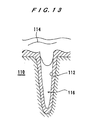
- FIG. 13 shows the results of filling copper into a minute via formed in a surface of a semiconductor substrate using a copper target of large grains whose diameter is approximately 200 ⁇ m, obtained by annealing thereof at a high temperature described above.
- copper 114 is not deposited in the interior of a via 112 having a diameter of approximately 0.15 ⁇ m, formed in the surface of the semiconductor substrate 110, except for an inlet portion of the via 112, and the upper part of the via 112 is blockaded while leaving a void 116. Therefore, it is difficult or impossible to form copper wiring or interconnects having sufficient current capacity. This is presumably caused by oblique traveling characteristic of copper atoms which have been sputtered.
- the optimum process consists of formation of the seed layer by sputter deposition, followed by copper electroplating metalization.
- the primary purpose of the seed layer is that the seed layer serves as an electrolytic cathode for supplying a sufficient amount of current to reduce metal ions in the plating liquid and to precipitate and deposit solid metal on the substrate. This is because as long as the seed layer remains satisfactory, there exists a high possibility of simultaneously realizing three factors; excellent filling property, high conductivity, and electromigration resistance with electroplating.
- a thin seed layer of conductive material uniformly and continuously over the entire inner surface of the recess.
- a thin seed layer of the same material as wiring material, i.e. copper is formed prior to electroplating.
- the deposited material in some cases, forms a less uniform thickness layer, which is less conformable to the underlayer, and forms a granular, rough surface.
- This behavior can be explained in terms of surface diffusion of the deposited material depending on the interaction between the thin film and the underlayer material, and the elevated temperature.
- aluminum or aluminum alloy is deposited relatively easily and uniformly on a barrier layer of TaN or TiN or the like by sputter deposition.
- sputtered and deposited copper atoms normally agglomerate on the barrier layer of TaN or TiN or the like during high temperature sputter deposition process to thus form a granular and discontinuous film, rarely producing a thin and uniform thickness deposition. If copper atoms agglomerate on a large scale to form nonuniform copper seed layer on the barrier layer, the plating current flowing through the seed layer becomes insufficient.
- the seed layer has film defect, it is impossible to cause plating current to flow through such defective portion.
- a defective plated portion is liable to develop on an incomplete seed layer in the subsequent plating process. This holds true for electroless plating on a catalytic layer as an underlying layer, in place of the seed layer for the electroplating.
- the substrate is cooled during sputter deposition at a low temperature to prevent an improper surface diffusion.
- the substrate cooling might not necessarily work in present sputtering apparatuses.
- Another object of the present invention is to provide a method and apparatus for forming interconnect, and a target material which can suppress oblique traveling characteristic of sputtered atoms, cause the sputtered atoms to enter the deepest portion of a minute recess formed in the surface of the substrate, and coat or fill a conductive material into the interior of the minute recess without generating a defective portion or void.
- Still another object of the present invention is to provide a method and apparatus for forming an underlying layer having a uniform thickness by suppressing generation of agglomeration on an interior surface of a minute recess, and forming satisfactory interconnect embedded in the recess and having no effect.
- a method for forming interconnect on a substrate by filling a conductive material in a fine recess formed in a surface of the substrate comprising: providing a substrate and a target composed of a conductive material in confrontation with each other in a chamber; introducing a sputtering gas into the chamber while a high voltage is applied between the substrate and the target to cause the sputtering gas to collide with the target; and depositing particles of the conductive material emitted from the target on the surface of the substrate to form a thin film, while sputter-etching the thin film by reflection sputtering gas molecules reflected from the target and having high energy.
- neutral reflection sputtering gas molecules are mixed with the conductive material particles emitted from the target and collide with the surface of the substrate to thus perform sputter etching of the conductive material layer deposited on the surface of the substrate, particularly, the conductive material deposited in a relatively thick state on the portion near the inlet of the fine recess (typically the overhang portion A in FIG. 10) preferentially. Therefore, the conductive material particles enter the interior and the depth of the recess and easily deposited therein.
- the potential difference E between the substrate and the target is set to 30/A or more, and the sputtering gas such as argon gas which has been introduced into the chamber is ionized and accelerated by the electric field to form high-energy particles. Then, a part of the high-energy particles is neutralized and reflected from the surface of the target and becomes neutral reflection sputtering gas molecules having a sufficiently high energy for sputter etching. Further, the potential difference E between the substrate and the target is set to 500/A or less, thus preventing silicon semiconductor devices from being damaged.
- the distance L between the substrate and the target is set to the mean free path ⁇ or less, and hence the limited distance L mostly suppresses scattering caused by collision of the neutral reflection sputtering gas molecules with each other or resultant attenuation of kinetic energy.
- the sputter etching action of the neutral reflection sputtering gas molecules is prevented from being reduced.
- the distance L between the substrate and the target set to 400 mm or less prevents the conductive material particles which reach the substrate from being reduced.
- the distance L between the substrate and the target set to 50 mm or more avoids the damage to semiconductor devices caused by collision of the high energy conductive material particles or secondary electrons.
- the sputtering gas comprises argon gas, and a pressure P (Pa) in the chamber is set to a range which satisfies P ⁇ 6.77/L.
- the sputtering gas comprises argon gas
- the target comprises copper
- the potential difference E between the substrate and the target is in the range of 0.6 to 10 kV.
- the substrate comprises a semiconductor substrate
- the target comprises copper, tantalum, titanium, tungsten, or alloy or compound containing at least one of these elements.
- an apparatus for forming interconnect on a substrate by filling a conductive material in a fine recess formed in a surface of the substrate comprising: a chamber for providing a substrate and a target composed of a conductive material in confrontation with each other therein; a power supply for applying a high voltage between the substrate and the target; and a gas introducing passage for introducing a sputtering gas into the chamber to cause the sputtering gas to collide with the target; wherein particles of the conductive material emitted from the target by collision of the sputtering gas are deposited on the surface of the substrate to form a thin film, while sputter-etching the thin film by reflection sputtering gas molecules reflected from the target and having high energy.
- the sputtering gas comprises argon gas, and a pressure P (Pa) in the chamber is set to a range which satisfies P ⁇ 6.77/L.
- the sputtering gas comprises argon gas
- the target comprises copper
- the potential difference E between the substrate and the target is in the range of 0.6 to 10 kV.
- a method for forming interconnect on a substrate by filling a conductive material in a fine recess formed in a surface of the substrate comprising: providing a substrate and a target composed of a conductive material having crystal grains whose diameter is not greater than 70 ⁇ m in confrontation with each other in a chamber; introducing a sputtering gas into the chamber while a high voltage is applied between the substrate and the target to cause the sputtering gas to collide with the target; and depositing particles of the conductive material emitted from the target by collision of the sputtering gas on the surface of the substrate to form a thin film.
- the target comprising a conductive material having crystal grains whose diameter is equal to or less than 70 ⁇ m
- the target contains many crystal grains having various crystal orientations, and the conductive material particles (sputtered atoms) can be emitted from the target toward various directions.
- the conductive material particles which travel in oblique directions collide with each other and the random traveling directions of the conductive material particles can be relaxed and averaged.
- the voltage applied between the substrate and the target is equal to or more than 1000 V.
- a relatively high voltage is applied between the substrate and the target comprising a conductive material having crystal grains whose diameter is equal to or less than 70 ⁇ m, the conductive material particles emitted from the target toward every direction interfere with each other and are averaged on the whole, and mainly the conductive material particles which travel in a vertical direction (direction perpendicular to the surface of the substrate) reach the substrate.
- the applied voltage between the substrate and the target is equal to or higher than 1000 V
- the effect of the target having small crystal grains is remarkable due to the intensified etching rate by the reflection sputtering gas molecules.
- a method for forming interconnect on a substrate by filling a conductive material in a fine recess formed in a surface of the substrate comprising: providing a substrate and a target composed of a conductive material having crystal grains whose diameter is not greater than 60 ⁇ m in confrontation with each other in a chamber; introducing a sputtering gas into the chamber while a high voltage is applied between the substrate and the target to cause the sputtering gas to collide with the target; and depositing particles of the conductive material emitted from the target by collision of the sputtering gas on the surface of the substrate to form a thin film.
- the number of crystal grains having various crystal orientations increases, and the conductive material particles (sputtered atoms) can be emitted from the target toward more various directions.
- the voltage applied between the substrate and the target is equal to or more than 1000 V.
- a high voltage which is equal to or more than 1000 V is applied between the substrate and the target comprising crystal grains whose diameter is not more than 60 ⁇ m.
- the above effect is further promoted.
- an apparatus for forming interconnect on a substrate by filling a conductive material in a fine recess formed in a surface of the substrate comprising: a chamber for providing a substrate and a target composed of a conductive material having crystal grains whose diameter is not greater than 70 ⁇ m in confrontation with each other therein; a power supply for applying a high voltage between the substrate and the target; and a gas introducing passage for introducing a sputtering gas into the chamber to cause the sputtering gas to collide with the target; wherein particles of the conductive material emitted from the target by collision of the sputtering gas are deposited on the surface of the substrate to form a thin film.
- the voltage applied between the substrate and the target is equal to or more than 1000 V.
- an apparatus for forming interconnect on a substrate by filling a conductive material in a fine recess formed in a surface of the substrate comprising: a chamber for providing a substrate and a target composed of a conductive material having crystal grains whose diameter is not greater than 60 ⁇ m in confrontation with each other therein; a power supply for applying a high voltage between the substrate and the target; and a gas introducing passage for introducing a sputtering gas into the chamber to cause the sputtering gas to collide with the target; wherein particles of the conductive material emitted from the target by collision of the sputtering gas are deposited on the surface of the substrate to form a thin film.
- the voltage applied between the substrate and the target is equal to or more than 1000 V.
- a target material for use in a target provided in an apparatus for forming interconnect on a substrate the target emitting particles by causing a sputtering gas to collide with the target, the particles being deposited on the surface of the substrate to form a thin film
- the target material comprising: a conductive material having crystal grains whose diameter is equal to or less than 70 ⁇ m.
- the conductive material comprises one of copper and copper alloys.
- a target material for use in a target provided in a apparatus for forming interconnect on a substrate the target emitting particles by causing a sputtering gas to collide with the target, the particles being deposited on the surface of the substrate to form a thin film
- the target material comprising: a conductive material having crystal grains whose diameter is equal to or less than 60 ⁇ m.
- the conductive material comprises one of copper and copper alloys.
- a method for forming interconnect on a substrate by filling a first conductive material in a fine recess formed in a surface of the substrate with plating comprising: forming an underlying layer comprising a second conductive material having surface energy lower than that of the first conductive material on an interior surface of said recess; and plating the surface of the substrate with the first conductive material.
- the seed layer when the underlying layer as a seed layer is formed by film deposition by sputtering, the seed layer is formed by a conductive material which is hard to be agglomerated or granulated by temperature rise, compared with the conductive material for forming the main conductor.
- the seed layer is prevented from being granulated, or the degree of granulation of the seed layer is reduced.
- improper plating or generation of plating defect can be prevented.
- the second conductive material comprises alloy containing at least one element constituting the first conductive material.
- the first conductive material comprises copper
- the second conductive material comprises alloy containing copper
- the underlying layer having a uniform thickness and having no agglomeration and granulation is formed by sputter deposition, for example, and satisfactory interconnects comprising copper and having no defect can be formed.
- the alloy containing the copper comprises copper-nickel alloy containing at least 5 % nickel.
- alloy is prepared by adding nickel to copper, as nickel content increases from zero to a certain percentage, surface energy decreases.
- copper-nickel alloy containing at least 5 % nickel can form an underlying layer having no granulation or agglomeration.
- an interconnect structure comprising: a fine recess formed in a surface of a substrate; interconnect comprising a conductive material filled in the fine recess; and an underlying layer formed on the recess and underlying the interconnect, the underlying layer comprising a conductive material having lower surface energy than the conductive material for forming the interconnect.
- FIG. 1 shows a DC dual electrode magnetron sputtering apparatus for forming interconnects according to an embodiment of the present invention.
- argon gas which is generally used as sputtering gas is used and interconnects are formed by sputter deposition of copper in an argon gas atmosphere will be described below.
- the tool for forming interconnects has a chamber 1, and a vertically movable substrate holder 3 for holding a substrate 2 and a target 4 are disposed in confrontation with each other in the chamber 1. Magnets 5 are provided below the target 4 to form magnetic field in the chamber 1.
- the interior of the chamber 1 is connected to a vacuum pump (not shown) such as an oil diffusion vacuum pump through an exhaust port 6, and connected to an argon gas source 7 through a flow regulating valve 8.
- the target 4 is composed of conductive material comprising copper (Cu) in this embodiment, and connected to a cathode of variable output voltage type of a DC power source 10.
- the substrate holder 3 is grounded.
- a tube 9 which allows a heating medium or a cooling medium for heating or cooling the substrate 2 to pass therethrough is connected to the substrate holder 3.
- the substrate 2 may be heated by a heater embedded in the substrate holder 3.
- a shutter 11 which is freely openable and closable is disposed below the substrate holder 3.
- the distance L between the substrate holder 3 and the target 4 is set to 250 mm, the target 4 has a diameter of 120 mm, and the substrate holder 3 has a diameter of 100 mm.
- the interior of the chamber 1 is evacuated by the vacuum pump, negative high-voltage of direct current is applied to the target 4 by the DC power source 10, and argon gas is introduced as sputtering gas into the chamber 1 through the flow regulating valve 8. Then, argon gas is ionized and accelerated in the electric field to form high-energy particles, and then the high-energy particles collide with the target 4. By this collision, copper atoms (conductive material particles) are sputtered and emitted from the target 4, and travel straight and are deposited on the surface of the substrate 2, thus forming a thin film (layer) of copper.
- copper atoms emitted from the target 4 are deposited on the surface of the substrate 2 to thus form a thin film of copper.
- copper 104 is deposited in a concentrated manner at the inlet portion of the minute recess 102a formed in the surface of the substrate 102, thus forming the overhang portion (projecting portion) A.
- copper atoms emitted from the target 4 are deposited in the interior of the recess 2a formed in the substrate 2 (see FIGS. 4A through 4C). Accordingly, copper 12 is coated and filled in the interior of the recess 2a, thus forming satisfactory copper interconnects having no defect such as void therein.
- argon gas introduced into the chamber 1 is ionized in the electric field and has high energy
- a part of argon gas becomes neutral reflection argon molecules (reflection sputtering gas molecules) after collision, with a considerable amount of kinetic energy, reflected from the surface of the target 4.
- the magnitude of kinetic energy of the neutral reflection argon molecules is proportional to the potential difference between the substrate 2 and the target 4, and depends on a scattering angle of the neutral reflection argon molecules.
- the kinetic energy of the neutral reflection argon molecules is in the range of 24 to 100 eV.
- the kinetic energy of the neutral reflection argon molecules largely depends on mass of the target 4.
- the kinetic energy of the neutral reflection argon molecules with a scattering angle of 180° after collision i.e., the kinetic energy E R of the neutral reflection argon molecules after head-on collision against the target and reflecting in a perpendicular direction to the surface of the target, is represented by the following equation: (4) [Kobayashi, H., and Hosokawa, N.
- the target 4 comprises copper
- the kinetic energy E R of the neutral reflection argon molecules equals 5 % of the kinetic energy E 1 of argon ions which collide with the target 4.
- the minimum value of ion energy required for sputtering solid target atoms is called threshold energy.
- This threshold energy for engineering metal targets ranges from 30 to 50 eV [Kobayashi, H. "Basic Sputtering Thin Film and Application Thereof", (The Nikkan Kogyo Shimbun, Ltd., April, 1998.) pp. 30-31.]. Therefore, in order to perform sputter etching with neutral reflection argon molecules, it is necessary that the ion energy E 1 is set to such a value that the kinetic energy E R of the neutral reflection argon molecules is equal to or greater than the threshold energy for the solid which is subject to sputter etching. Thus, it is necessary that the following equation (6) holds from the equation (5). E 1 ⁇ 600 eV
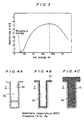
- FIG. 3 [Kobayashi, H. "Basic Sputtering Thin Film and Application Thereof", (The Nikkan Kogyo Shimbun, Ltd., April, 1998.) pp. 30-31.], [Kobayashi, H., and Hosokawa, N. "Introduction to Thin Film Technology", (Sougou Electronics Press, July, 1992.) p.60.]. As is apparent from FIG. 3 [Kobayashi, H., and Hosokawa, N. “Introduction to Thin Film Technology", (Sougou Electronics Press, July, 1992.) p.60.]. As is apparent from FIG.
- the applied voltage between the target and the substrate is approximately 60 kV.
- the applied voltage between the target 4 and the substrate 2 is lower than 60 kV and is mostly set to a value ranging from 300 to 2000 V [Kobayashi, H., and Hosokawa, N. "Introduction to Thin Film Technology", (Sougou Electronics Press, July, 1992.) p.60.].
- the applied voltage between the target and the substrate should be set to approximately 60 kV for the maximum sputtering yield and high energy of the neutral reflection argon molecules, respectively.
- the allowable energy of the particles which collide with the substrate 2 is equal to or less than 500 eV.
- Equation (7) means that energy E 1 of argon incident on the target is required to be equal to or less than 10 keV (apparent voltage (indicated value) between the target and the substrate is not more than 10 kV) E 1 ⁇ 10 keV
- the applied voltage between the target and the substrate is in the range of 0.6 kV to 10 kV as represented by the following equation (9), and in this range, the sputter etching can be reliably carried out and the semiconductor device can be prevented from being damaged.
- the operating voltage should be as low as possible to avoid any device damage, as long as circumstances permit.
- Practical dry etching apparatuses also need to use as low energy ions or plasma as possible for the same reason.
- the neutral reflection argon molecules (atoms) generated from the sputtering argon ions generated film the sputtering argon ions having kinetic energy expressed by the equation (8) are mixed with copper particles (atoms) and collide with the surface of the substrate 102 shown in a conventional example of FIG. 10, then the copper 104 deposited on the surface of the substrate 102 by film deposition by sputtering, particularly the copper 104 of the overhang portion A deposited in a relatively thick state on the portion near the inlet of the recess 102a is preferentially sputter-etched by the neutral reflection argon molecules. Accordingly, a certain part of the overhang portion A is removed. Thus, the coating and filling of copper progress smoothly into the interior and the depth of the recess 102a.
- the neutral reflection argon molecules need to travel straight after reflected by the target 4 and collide with the surface of the substrate 2.
- pressure in the chamber 1 is required to be set at such a value that the mean free path ⁇ of the neutral reflection argon molecules during process is equal to or greater than the distance L between the target 4 and the substrate 2.
- ⁇ 3.11 ⁇ 10 -24 (T/P ⁇ 2 )
- the pressure in the chamber 1 should be kept at such a value that the mean free path ⁇ (mm) in the equation (10) is equal to or greater than the distance L (mm) between the substrate 2 and the target 4.
- the following equation (11) holds. P ⁇ 6.77/L
- the distance L between the substrate 2 and the target 4 should be in the range of 50 to 400 mm. That is, as the distance L between the substrate 2 and the target 4 prolongs, the percentage of copper atoms which travel perpendicularly to the substrate increases, and hence this is advantageous in coating or filling of the fine recesses formed in the surface of the substrate 2.
- the maximum of the practical distance L between the substrate 2 and the target 4 is set to approximately 400 mm.
- the distance L between the substrate 2 and the target 4 is smaller, collision energy of secondary electrons which collide with the substrate grows larger to damage devices when L ⁇ 50 mm.
- the distance L between the substrate 2 and the target 4 needs to be in the range of 50 to 400 mm, and approximately 200 mm is optimum. That is, the following equation (12) holds. 50 mm ⁇ L ⁇ 400 mm
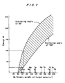
- the range of operating pressure in the sputter deposition process according to the present invention should be limited to the hatched area in the P-L (operating pressure vs. the distance between the substrate and the target) diagram of FIG. 5.
- the sputter deposition operating pressure P (Pa) according to the present invention is equal to or less than 1.35 ⁇ 10 -1 Pa when the distance L between the substrate and the target is 50mm, and is equal to or less than 1.69 ⁇ 10 -2 Pa when the distance L between the substrate and the target is 400 mm.
- FIGS. 4A through 4C The results in which copper is coated or filled in the recess 2a formed in the substrate 2 under the above conditions are schematically shown in FIGS. 4A through 4C. It was confirmed that as shown in FIGS. 4A through 4C, copper 12 was uniformly and continuously filled into the interior of the deep and fine recess 2a having a width of 0.15 ⁇ m or smaller without forming a void, and favorable interconnects of the copper 12 having no defect was obtained.
- the temperature of the substrate 2 was 200°C
- the pressure in the chamber 1 was 1 ⁇ 10 -1 Pa.
- the target 4 comprises copper
- the material of the target 4 is not limited to copper, and silver (Ag), tantalum (Ta), titanium (Ti), tungsten (W), or alloy or compound containing at least one of these elements may be used as the target 4.
- the semiconductor wafer is used as a substrate having a fine recess or recesses, the kind of substrate is not limited to the semiconductor wafer.
- Argon (Ar) gas is used as sputtering gas introduced into the chamber 1, but the kind of sputtering gas is not limited to argon gas. As long as gas is ionized and accelerated in the chamber 1 to form high energy particles, and does not adversely affect the substrate, any material may be used.
- neutral reflection argon molecules are mixed with the conductive material particles emitted from the target and collide with the surface of the substrate to thus perform sputter etching of the conductive material layer deposited on the surface of the substrate, particularly, the conductive material deposited in a relatively thick state on the portion near the inlet of the fine recess preferentially. Therefore, the conductive material particles enter the interior and the depth of the recess, and are easily deposited therein. Thus, the conductive material such as copper reliably fills in the interior of the recess, and the satisfactory interconnects having no defect such as void can be formed.
- the recess has a narrow width of, for example, 0.13 to 0.15 ⁇ m or less, such recess can be reliably coated and filled with copper, the conductive material, by sputter deposition, although such recess has not heretofore been filled by sputter deposition.
- copper having crystal grains whose diameter is not greater than 70 ⁇ m, and preferably not greater than 60 ⁇ m is used as a conductive material for a target.
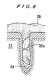
- FIG. 6 schematically shows the results in which copper having small crystal grains whose diameter was 62 ⁇ m was used as the target 4, and copper was coated and filled in the recess 22a formed in the substrate 22 under the normal condition.
- copper 26 is filled in almost entire depth of the deep and fine recess 22a having a diameter of about 0.15 ⁇ m or smaller while leaving a small void 24 at the deepest portion. It is considered that this is caused by the fact that since the crystal grains of the target 4 become extremely small, there is a strong tendency that copper atoms are sputtered in various traveling directions in accordance with crystal orientation of the respective crystal grains.
- the copper atoms are emitted in various traveling directions, the copper atoms collide with each other and interfere with each other (the phenomenon similar to elastic scattering), with high frequency.
- random traveling directions of copper atoms are averaged, and on the whole, relatively many copper atoms which travel in a direction normal to the surface of the target 4 and the surface of the substrate 22 reach the substrate 22.
- filling characteristic to the fine recess 22a formed in the substrate 22 is improved.
- crystal grains of various crystal orientations are finer, the effect of averaging of the random traveling directions of copper atoms are more remarkably averaged.
- sputtering gas ions here, argon gas ions
- the surface of the target 4 is subject to repetitive cycles of heating and cooling in the range from ambient temperature to the maximum temperature of 550°C due to repeating operation of the apparatus for forming interconnects, the surface of the target 4 is physically etched (eroded) due to the alternating impacts (microscopically strained) caused by argon ions, thus being subjected to severe hysteresis of damage.
- the portion near the surface of the target 4 is subject to heat hysteresis, a part of which is similar to the heat hysteresis caused by annealing. Therefore, even if the diameter of crystal grains on the top surface of the target 4 is large at the initial stage, the diameter of crystal grains tends to converge on a range determined by the temperature of annealing, i.e., 550°C shown in FIG. 12, and thus the range of 50 to 60 ⁇ m.
- the diameter of crystal grains at the initial stage is larger than 50 to 60 ⁇ m, the effect of averaging of random traveling directions of copper atoms is poor and the crystal grains are subjected to thermal load, which gradually changes the crystal grain diameters to a stable size shown in FIG. 12. Thus, the directions of sputtered copper atoms are influenced by this grain size variation and are extremely unstable.
- the diameter of crystal grains at the initial stage is smaller than 50 to 60 ⁇ m, traveling directions of the copper atoms are averaged from the initial stage and the diameter of crystal grains gradually grows, and finally the diameter of the crystal grains becomes in the range of 50 to 60 ⁇ m.
- the direction of the sputtered atoms is held in a direction perpendicular to the surface of the target 4.
- coating and filling of copper progress stably in a steady state, and the sputtered copper atoms reach the deepest portion of the fine recess 22a formed in the surface of the substrate 22 and are deposited therein.
- the applied voltage between the substrate 2 and the target 4 is normally considered to be less than 1000 V, for example, approximately 400 V.
- the applied voltage between the substrate 2 and the target 4 is preferably higher than the above mentioned normal voltage, for instance, in the case where a material of the target 4 is coated, or filled in the interior of the recess formed in the substrate 2 to metalize semiconductor devices.
- the present invention exhibits remarkable effect in the case where the applied voltage between the substrate 2 and the target 4 (see FIG. 1) is considerably higher than the normal voltage, particularly the applied voltage is not less than 1000 V.
- conductive materials constituting the target 4 copper having crystal grains whose diameter is not more than 70 ⁇ m, preferably not more than 60 ⁇ m is used.
- other copper alloy or conductive material may be used, as long as the diameter of crystal grains is not more than 70 ⁇ m, preferably not more than 60 ⁇ m.
- the substrate 2 is not limited to a semiconductor substrate, and any substrate having fine recess or recesses for interconnects may be used.
- the sputtering gas is not limited to argon gas.
- the conductive material composed of crystal grains whose diameter is not more than 70 ⁇ m, preferably not more than 60 ⁇ m is used as the target material, and hence oblique traveling characteristic of conductive particles which have been sputtered is suppressed on the whole, and the conductive particles enter the deepest portion of the fine recess formed in the surface of the substrate and are deposited therein. Therefore, the conductive material such as copper can be reliably coated and filled in the recess to enable satisfactory interconnects having no defect such as void.
- the recess has a narrow width of, for example, 0.13 to 0.15 ⁇ m or less, such recess can be reliably coated and filled with the conductive material of copper by film deposition by sputtering, although such recess has not heretofore been filled by conventional film deposition by sputtering.
- FIGS. 7A through 7C show successive steps of manufacturing copper interconnects for a semiconductor.
- an oxide film 32 of SiO 2 is deposited on a conductive layer 31a on a semiconductor substrate 31 on which semiconductor devices are formed.
- a fine recess 35 comprising a via hole 33 and a trench 34 for a predetermined interconnect pattern in the oxide film 32 by lithography and etching.
- a barrier layer 36 of TaN or the like is formed, and then a seed layer 37 to supply electric current for electroplating is formed on the barrier layer 36 by film deposition by sputtering.
- the entire surface of the semiconductor substrate W is coated with copper by electroplating to deposit a copper layer 38 on the entire surface, thus filling the recess 35 with copper.
- the copper layer 38 on the barrier layer 36 and the barrier layer 36 are removed by chemical mechanical polishing (CMP), thus making the copper layer 38 in the via hole 33 and the trench 34 lie flush with the oxide film 32.
- CMP chemical mechanical polishing
- the seed layer 37 is composed of a material having surface energy which is lower than that of the material for forming the interconnect 39, i.e. copper.
- the seed layer 37 is composed of copper-nickel alloy containing at least 10 % nickel.
- the seed layer is formed with pure copper which is the same material as that for interconnects.
- pure copper is deposited on the barrier layer comprising TaN or the like by film deposition by sputtering to form the seed layer, copper atoms are agglomerated at a high temperature to form granular rough surface, and it is difficult to obtain a continuous and thin film having a uniform thickness.
- the seed layer is formed with copper-nickel alloy containing at least 10 % nickel, and hence the thin film (seed layer) having a uniform thickness can be obtained.
- the mechanism In the case where the metal is agglomerated at a high temperature on the surface of the substrate to change its shape into a granular shape, the mechanism generally involves various complicated factors including external factors such as a temperature of substrate, a temperature, concentration, pressure, or flow rate of gas, or the like, and internal factors such as property of the substrate or metal deposited on the substrate, and the degree of interaction between the metal and the substrate.
- external factors such as a temperature of substrate, a temperature, concentration, pressure, or flow rate of gas, or the like
- internal factors such as property of the substrate or metal deposited on the substrate, and the degree of interaction between the metal and the substrate.
- only specific surface energy of the deposited metal is taken into consideration, because the sputter deposition behavior is well interpreted in terms of the minimum surface energy concept, i.e., high surface energy materials have a strong tendency to cause large scale agglomeration or granulation to decrease the sum total of the surface area of the deposited material.
- the surface energy of two kinds of Cu-Ni alloys can be calculated from the surface energy of copper, the equation (14), and the values listed in Table 1. The results of the calculation are listed in Table 2. (approximate)composition Surface energy 100%Cu 1,670erg/cm 2 10%Ni-Cu 1,493 67%Ni-Cu 1,026
- a curved line shown in FIG. 8 represents a lowering tendency of the surface energy (see Table 2) in accordance with increase of a nickel content. Specifically, FIG. 8 shows that the lowered surface energy corresponds with no agglomeration. Therefore, it is adequate to predict depending on the surface energy of materials as a proper measure whether deposited atoms are agglomerated and granulated or not.
- FIG. 9 shows a schematic illustration of an electroplating cell used to plate metal on a semiconductor wafer.
- ⁇ c represents the electric resistivity of a cathode (seed layer)
- ⁇ a represents that of an anode (Cu-P alloy)
- ⁇ l represents that of a plating liquid.
- the electric resistivity ⁇ l of the plating liquid is about 1,000,000 times larger than ⁇ c and ⁇ a, the electric resistivity of the cathode and the anode, respectively.
- the electrical resistance of the plating liquid occupies substantially 100 % of the electric resistance of the whole circuit.
- a nickel content can be determined substantially independently of the electric resistivity increase which is caused by adding nickel to pure copper.
- an amount of nickel to be added to pure copper can simply be determined based on the graph shown in FIG. 8.
- an allowable lower limit of the nickel content is 5 %.
- the nickel content should preferably be 10 % or higher.
- the seed layer is formed of Cu-Ni alloy.
- copper may be alloyed with a metallic element other than nickel to form the seed layer.
- any other metallic material may be used to form the seed layer.
- usual engineering metals have extremely smaller electric resistivity than the plating liquid, a large variety of metals may be used to form the seed layer.
- granulation of the seed layer can be avoided, or the degree of granulation of the seed layer can be suppressed to form the continuous seed layer (underlying layer) having a uniform thickness on an inner circumferential surface of a minute recess. Therefore, improper plating or plating defect in a subsequent plating process can be prevented.
Landscapes
- Chemical & Material Sciences (AREA)
- Engineering & Computer Science (AREA)
- Organic Chemistry (AREA)
- Materials Engineering (AREA)
- Mechanical Engineering (AREA)
- Metallurgy (AREA)
- Chemical Kinetics & Catalysis (AREA)
- Physics & Mathematics (AREA)
- Plasma & Fusion (AREA)
- Analytical Chemistry (AREA)
- Internal Circuitry In Semiconductor Integrated Circuit Devices (AREA)
- Electrodes Of Semiconductors (AREA)
- Physical Vapour Deposition (AREA)
Applications Claiming Priority (8)
| Application Number | Priority Date | Filing Date | Title |
|---|---|---|---|
| JP2000014919 | 2000-01-24 | ||
| JP2000014919A JP2001210643A (ja) | 2000-01-24 | 2000-01-24 | 配線形成方法及び配線構造 |
| JP2000030422A JP3699625B2 (ja) | 2000-02-08 | 2000-02-08 | 基材の配線形成方法 |
| JP2000030422 | 2000-02-08 | ||
| JP2000039661A JP2001230218A (ja) | 2000-02-17 | 2000-02-17 | スパッタリングによる配線形成方法、配線形成装置及びそのターゲット材料 |
| JP2000039661 | 2000-02-17 | ||
| JP2000335906 | 2000-11-02 | ||
| JP2000335906A JP2002146526A (ja) | 2000-11-02 | 2000-11-02 | 基材の配線形成方法及び装置 |
Publications (2)
| Publication Number | Publication Date |
|---|---|
| EP1120820A2 true EP1120820A2 (de) | 2001-08-01 |
| EP1120820A3 EP1120820A3 (de) | 2008-01-09 |
Family
ID=27480949
Family Applications (1)
| Application Number | Title | Priority Date | Filing Date |
|---|---|---|---|
| EP01101436A Withdrawn EP1120820A3 (de) | 2000-01-24 | 2001-01-23 | Verfahren und Vorrichtung zur Herstellung einer Verdrahtungsstruktur |
Country Status (2)
| Country | Link |
|---|---|
| US (1) | US6458694B2 (de) |
| EP (1) | EP1120820A3 (de) |
Families Citing this family (21)
| Publication number | Priority date | Publication date | Assignee | Title |
|---|---|---|---|---|
| US6355561B1 (en) * | 2000-11-21 | 2002-03-12 | Micron Technology, Inc. | ALD method to improve surface coverage |
| JP3972988B2 (ja) * | 2003-09-17 | 2007-09-05 | 沖電気工業株式会社 | 半導体装置の製造方法 |
| US6992389B2 (en) * | 2004-04-28 | 2006-01-31 | International Business Machines Corporation | Barrier for interconnect and method |
| JP4298597B2 (ja) * | 2004-07-01 | 2009-07-22 | 日東電工株式会社 | 配線回路基板および配線回路基板の製造方法 |
| US7844101B2 (en) * | 2005-01-31 | 2010-11-30 | Applied Materials Israel, Ltd. | System and method for performing post-plating morphological Cu grain boundary analysis |
| US12444651B2 (en) | 2009-08-04 | 2025-10-14 | Novellus Systems, Inc. | Tungsten feature fill with nucleation inhibition |
| US9312260B2 (en) * | 2010-05-26 | 2016-04-12 | Taiwan Semiconductor Manufacturing Company, Ltd. | Integrated circuits and manufacturing methods thereof |
| US9806252B2 (en) | 2015-04-20 | 2017-10-31 | Lam Research Corporation | Dry plasma etch method to pattern MRAM stack |
| US9870899B2 (en) | 2015-04-24 | 2018-01-16 | Lam Research Corporation | Cobalt etch back |
| US9972504B2 (en) | 2015-08-07 | 2018-05-15 | Lam Research Corporation | Atomic layer etching of tungsten for enhanced tungsten deposition fill |
| US10096487B2 (en) | 2015-08-19 | 2018-10-09 | Lam Research Corporation | Atomic layer etching of tungsten and other metals |
| US9984858B2 (en) | 2015-09-04 | 2018-05-29 | Lam Research Corporation | ALE smoothness: in and outside semiconductor industry |
| US10229837B2 (en) | 2016-02-04 | 2019-03-12 | Lam Research Corporation | Control of directionality in atomic layer etching |
| US10727073B2 (en) | 2016-02-04 | 2020-07-28 | Lam Research Corporation | Atomic layer etching 3D structures: Si and SiGe and Ge smoothness on horizontal and vertical surfaces |
| US9991128B2 (en) | 2016-02-05 | 2018-06-05 | Lam Research Corporation | Atomic layer etching in continuous plasma |
| US10269566B2 (en) | 2016-04-29 | 2019-04-23 | Lam Research Corporation | Etching substrates using ale and selective deposition |
| US9837312B1 (en) * | 2016-07-22 | 2017-12-05 | Lam Research Corporation | Atomic layer etching for enhanced bottom-up feature fill |
| US10566212B2 (en) | 2016-12-19 | 2020-02-18 | Lam Research Corporation | Designer atomic layer etching |
| KR102642011B1 (ko) | 2018-03-30 | 2024-02-27 | 램 리써치 코포레이션 | 내화성 금속들 및 다른 고 표면 결합 에너지 재료들의 원자 층 에칭 및 평활화 (smoothing) |
| GB2588945B (en) * | 2019-11-15 | 2024-04-17 | Dyson Technology Ltd | Method of depositing material on a substrate |
| CN117127154B (zh) * | 2023-10-16 | 2024-08-06 | 粤芯半导体技术股份有限公司 | 一种半导体器件中的互连金属的沉积方法 |
Family Cites Families (9)
| Publication number | Priority date | Publication date | Assignee | Title |
|---|---|---|---|---|
| CZ154293A3 (en) * | 1993-07-29 | 1995-02-15 | Fyzikalni Ustav Avcr | Process and apparatus for magnetron sputtering |
| US6030511A (en) * | 1995-02-03 | 2000-02-29 | Nec Corporation | Collimated sputtering method and system used therefor |
| JP2907267B2 (ja) * | 1995-02-03 | 1999-06-21 | 日本電気株式会社 | コリメータスパッタ法及び装置 |
| JPH10261772A (ja) * | 1997-01-14 | 1998-09-29 | Mitsubishi Electric Corp | 半導体記憶装置及びその製造方法 |
| US6387805B2 (en) * | 1997-05-08 | 2002-05-14 | Applied Materials, Inc. | Copper alloy seed layer for copper metallization |
| US6051114A (en) * | 1997-06-23 | 2000-04-18 | Applied Materials, Inc. | Use of pulsed-DC wafer bias for filling vias/trenches with metal in HDP physical vapor deposition |
| US6139701A (en) * | 1997-11-26 | 2000-10-31 | Applied Materials, Inc. | Copper target for sputter deposition |
| US6022808A (en) * | 1998-03-16 | 2000-02-08 | Advanced Micro Devices, Inc. | Copper interconnect methodology for enhanced electromigration resistance |
| US6113761A (en) * | 1999-06-02 | 2000-09-05 | Johnson Matthey Electronics, Inc. | Copper sputtering target assembly and method of making same |
-
2001
- 2001-01-23 US US09/767,145 patent/US6458694B2/en not_active Expired - Fee Related
- 2001-01-23 EP EP01101436A patent/EP1120820A3/de not_active Withdrawn
Also Published As
| Publication number | Publication date |
|---|---|
| US20020009883A1 (en) | 2002-01-24 |
| US6458694B2 (en) | 2002-10-01 |
| EP1120820A3 (de) | 2008-01-09 |
Similar Documents
| Publication | Publication Date | Title |
|---|---|---|
| US6458694B2 (en) | High energy sputtering method for forming interconnects | |
| US6627542B1 (en) | Continuous, non-agglomerated adhesion of a seed layer to a barrier layer | |
| US7294574B2 (en) | Sputter deposition and etching of metallization seed layer for overhang and sidewall improvement | |
| US7795138B2 (en) | Method of depositing a metal seed layer over recessed feature surfaces in a semiconductor substrate | |
| JP3193875B2 (ja) | 半導体ウェハにおけるコンタクト、ビア及びトレンチの低熱費金属の充填及び平坦化のための方法と装置 | |
| US6429523B1 (en) | Method for forming interconnects on semiconductor substrates and structures formed | |
| US6391163B1 (en) | Method of enhancing hardness of sputter deposited copper films | |
| US20060251872A1 (en) | Conductive barrier layer, especially an alloy of ruthenium and tantalum and sputter deposition thereof | |
| JP2004531053A (ja) | 銅バイアにおける高抵抗バリア原子薄層 | |
| KR100501460B1 (ko) | 이온화된금속으로부터증착된접착층을사용한반도체구조물내의홀충전방법 | |
| EP1115898A1 (de) | Tantalfilme und verfahren zu deren herstellung | |
| US20020093101A1 (en) | Method of metallization using a nickel-vanadium layer | |
| US20080156636A1 (en) | Homogeneous Copper Interconnects for BEOL | |
| KR100365061B1 (ko) | 반도체소자및반도체소자제조방법 | |
| US20030214039A1 (en) | Method for fabricating semiconductor device having tertiary diffusion barrier layer for copper line | |
| JP2003197743A (ja) | 半導体装置 | |
| Chen et al. | Sub-Quarter Micron Metallization Using Ionized Metal Plasma Technology |
Legal Events
| Date | Code | Title | Description |
|---|---|---|---|
| PUAI | Public reference made under article 153(3) epc to a published international application that has entered the european phase |
Free format text: ORIGINAL CODE: 0009012 |
|
| AK | Designated contracting states |
Kind code of ref document: A2 Designated state(s): AT BE CH CY DE DK ES FI FR GB GR IE IT LI LU MC NL PT SE TR |
|
| AX | Request for extension of the european patent |
Free format text: AL;LT;LV;MK;RO;SI |
|
| PUAL | Search report despatched |
Free format text: ORIGINAL CODE: 0009013 |
|
| AK | Designated contracting states |
Kind code of ref document: A3 Designated state(s): AT BE CH CY DE DK ES FI FR GB GR IE IT LI LU MC NL PT SE TR |
|
| AX | Request for extension of the european patent |
Extension state: AL LT LV MK RO SI |
|
| AKX | Designation fees paid | ||
| STAA | Information on the status of an ep patent application or granted ep patent |
Free format text: STATUS: THE APPLICATION IS DEEMED TO BE WITHDRAWN |
|
| 18D | Application deemed to be withdrawn |
Effective date: 20080710 |
|
| REG | Reference to a national code |
Ref country code: DE Ref legal event code: 8566 |