EP1117147B1 - Lightning protection for an active antenna using patch/microstrip elements - Google Patents
Lightning protection for an active antenna using patch/microstrip elements Download PDFInfo
- Publication number
- EP1117147B1 EP1117147B1 EP01100096A EP01100096A EP1117147B1 EP 1117147 B1 EP1117147 B1 EP 1117147B1 EP 01100096 A EP01100096 A EP 01100096A EP 01100096 A EP01100096 A EP 01100096A EP 1117147 B1 EP1117147 B1 EP 1117147B1
- Authority
- EP
- European Patent Office
- Prior art keywords
- antenna elements
- patch antenna
- drain lines
- ground plane
- patch
- Prior art date
- Legal status (The legal status is an assumption and is not a legal conclusion. Google has not performed a legal analysis and makes no representation as to the accuracy of the status listed.)
- Expired - Lifetime
Links
- 230000003068 static effect Effects 0.000 claims abstract description 22
- 238000010168 coupling process Methods 0.000 claims description 10
- 230000008878 coupling Effects 0.000 claims description 9
- 238000005859 coupling reaction Methods 0.000 claims description 9
- 229910052751 metal Inorganic materials 0.000 claims description 9
- 239000002184 metal Substances 0.000 claims description 9
- 239000000758 substrate Substances 0.000 claims description 9
- 238000000034 method Methods 0.000 claims description 7
- 230000010287 polarization Effects 0.000 description 9
- 230000005855 radiation Effects 0.000 description 9
- 239000003990 capacitor Substances 0.000 description 4
- 230000000694 effects Effects 0.000 description 4
- 230000005540 biological transmission Effects 0.000 description 3
- 230000002411 adverse Effects 0.000 description 2
- 230000001413 cellular effect Effects 0.000 description 2
- 238000001125 extrusion Methods 0.000 description 2
- 238000007667 floating Methods 0.000 description 2
- 210000000554 iris Anatomy 0.000 description 2
- KENZYIHFBRWMOD-UHFFFAOYSA-N 1,2-dichloro-4-(2,5-dichlorophenyl)benzene Chemical compound ClC1=CC=C(Cl)C(C=2C=C(Cl)C(Cl)=CC=2)=C1 KENZYIHFBRWMOD-UHFFFAOYSA-N 0.000 description 1
- 229910052782 aluminium Inorganic materials 0.000 description 1
- XAGFODPZIPBFFR-UHFFFAOYSA-N aluminium Chemical compound [Al] XAGFODPZIPBFFR-UHFFFAOYSA-N 0.000 description 1
- 238000003491 array Methods 0.000 description 1
- 230000015556 catabolic process Effects 0.000 description 1
- 238000004891 communication Methods 0.000 description 1
- 239000004020 conductor Substances 0.000 description 1
- 238000010276 construction Methods 0.000 description 1
- 238000010586 diagram Methods 0.000 description 1
- 239000003989 dielectric material Substances 0.000 description 1
- 230000003993 interaction Effects 0.000 description 1
- 239000007769 metal material Substances 0.000 description 1
- 229920006395 saturated elastomer Polymers 0.000 description 1
- 238000007493 shaping process Methods 0.000 description 1
Images


Classifications
-
- H—ELECTRICITY
- H01—ELECTRIC ELEMENTS
- H01Q—ANTENNAS, i.e. RADIO AERIALS
- H01Q13/00—Waveguide horns or mouths; Slot antennas; Leaky-waveguide antennas; Equivalent structures causing radiation along the transmission path of a guided wave
- H01Q13/08—Radiating ends of two-conductor microwave transmission lines, e.g. of coaxial lines, of microstrip lines
-
- H—ELECTRICITY
- H01—ELECTRIC ELEMENTS
- H01Q—ANTENNAS, i.e. RADIO AERIALS
- H01Q3/00—Arrangements for changing or varying the orientation or the shape of the directional pattern of the waves radiated from an antenna or antenna system
- H01Q3/26—Arrangements for changing or varying the orientation or the shape of the directional pattern of the waves radiated from an antenna or antenna system varying the relative phase or relative amplitude of energisation between two or more active radiating elements; varying the distribution of energy across a radiating aperture
- H01Q3/28—Arrangements for changing or varying the orientation or the shape of the directional pattern of the waves radiated from an antenna or antenna system varying the relative phase or relative amplitude of energisation between two or more active radiating elements; varying the distribution of energy across a radiating aperture varying the amplitude
-
- H—ELECTRICITY
- H01—ELECTRIC ELEMENTS
- H01Q—ANTENNAS, i.e. RADIO AERIALS
- H01Q1/00—Details of, or arrangements associated with, antennas
- H01Q1/002—Protection against seismic waves, thermal radiation or other disturbances, e.g. nuclear explosion; Arrangements for improving the power handling capability of an antenna
-
- H—ELECTRICITY
- H01—ELECTRIC ELEMENTS
- H01Q—ANTENNAS, i.e. RADIO AERIALS
- H01Q1/00—Details of, or arrangements associated with, antennas
- H01Q1/12—Supports; Mounting means
- H01Q1/22—Supports; Mounting means by structural association with other equipment or articles
- H01Q1/24—Supports; Mounting means by structural association with other equipment or articles with receiving set
- H01Q1/241—Supports; Mounting means by structural association with other equipment or articles with receiving set used in mobile communications, e.g. GSM
- H01Q1/246—Supports; Mounting means by structural association with other equipment or articles with receiving set used in mobile communications, e.g. GSM specially adapted for base stations
-
- H—ELECTRICITY
- H01—ELECTRIC ELEMENTS
- H01Q—ANTENNAS, i.e. RADIO AERIALS
- H01Q1/00—Details of, or arrangements associated with, antennas
- H01Q1/50—Structural association of antennas with earthing switches, lead-in devices or lightning protectors
-
- H—ELECTRICITY
- H01—ELECTRIC ELEMENTS
- H01Q—ANTENNAS, i.e. RADIO AERIALS
- H01Q21/00—Antenna arrays or systems
- H01Q21/06—Arrays of individually energised antenna units similarly polarised and spaced apart
- H01Q21/08—Arrays of individually energised antenna units similarly polarised and spaced apart the units being spaced along or adjacent to a rectilinear path
-
- H—ELECTRICITY
- H01—ELECTRIC ELEMENTS
- H01Q—ANTENNAS, i.e. RADIO AERIALS
- H01Q23/00—Antennas with active circuits or circuit elements integrated within them or attached to them
-
- H—ELECTRICITY
- H01—ELECTRIC ELEMENTS
- H01Q—ANTENNAS, i.e. RADIO AERIALS
- H01Q9/00—Electrically-short antennas having dimensions not more than twice the operating wavelength and consisting of conductive active radiating elements
- H01Q9/04—Resonant antennas
- H01Q9/0407—Substantially flat resonant element parallel to ground plane, e.g. patch antenna
Definitions
- This invention is directed generally to the field of antennas for communication systems, and more particularly to a novel active antenna system using patch/microstrip antenna elements, and more particularly still, to a novel lightning, corona, and low frequency static energy protection scheme for such an antenna system.
- WO 97/43799 discloses a flat aperture-coupled antenna with a multiplayer structure, A rear side of the antenna comprises a metal reflector device including a hollow structure with separate box-like compartments, located in registery with radiating patches, corresponding pairs of orthogonal slots and feed elements, whereby microwave propagation within the hollow metal structure is substantially interrupted and any mutual coupling between the orthogonal slots is avoided.
- the invention is described herein in connection with an aperture coupled microstrip patch antenna used in a base station sector antenna with active electronics; however, the invention is not so limited, but may be used in connection with patch antenna elements in other applications.
- the radiating microstrip patch is located on a dielectric superstrate and the DC voltage of the (metal) patch is floating with respect to zero potential or ground. If a static charge develops on the (metal) patch and discharges through the aperture to the microstrip feeder line, damage to, or failure of, the active electronics connected to the microstrip feeder line is possible. Since the antenna is operating with a single polarization, e.g., vertical polarization, any DC connection to the patch in the opposite polarization, e.g., horizontal polarization, does not affect the desired radiation pattern.
- the present invention consists in an active antenna system having the features according to independent claim 1.
- the present invention consists in a method having the steps according to independent claim 13.
- the invention provides a narrow, high impedance conductive trace attached to the radiating patch in the orthogonal polarization (i.e., orthogonal to the patch polarization).
- These conductive traces are tied together with a vertical conductive trace along the axis of the array, which at a convenient location, is tied to an electrical ground.
- this grounding system of conductive traces is placed on the superstrate, so that the conductive traces do not disturb the base station's radiation pattern or VSWR (voltage standing wave ratio).
- VSWR voltage standing wave ratio
- the vertical trace is separated from the radiating patch. In one example of the invention, the vertical trace is roughly 0.45 ⁇ o (0.45 of a free space wavelength) away from the edge of the radiating patch.
- Some of the desirable effects to the (azimuth) radiation pattern are: (a) to suppress backward radiation, and, (b) shaping of the pattern within the sector coverage, i.e., tailoring the pattern to roll off quicker past the sector edge.
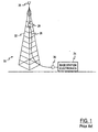
- FIG. 1 shows a conventional arrangement for a Cellular or PCS base station 20 having a tower 22 with a passive antenna 25 and ground-based electronics 24 connected to the antenna 25 by an RF cable 26.
- Lightning arrestor(s) 28, 30 are used either after the antenna at the tower top or at the base station, before the electronics, or both.
- the arrestors 28, 30 are high voltage capacitors wired in series with the RF cable 26. This prevents low frequency or DC current, associated with the absorbed corona energy, from a near miss lightning strike, from traveling through the RF coaxial cable into the base station electronics.
- FIG. 2 shows a side view, partially in section, of a typical patch antenna system 40, using an array of patch antenna elements (or “plates”) 42 and aperture coupling of the patch antenna elements 42 to a corporate feed 44, at apertures (irises) 46 in a ground plane 48.
- the corporate feed 44 shown here as a stripline structure
- the corporate feed would be in the same plane as the stripline coupling to the patches, etched on the same substrate (not shown in FIG. 2).
- the corporate feed could also be applied as a coaxial (cable) structure.
- the final feed output is connected to the coaxial cable 26 which traverses the tower 25 (FIG. 1) by a connector 52.
- the conventional lightning arrestors 28, 30 At the top and base of the tower 25 are the conventional lightning arrestors 28, 30. As mentioned above, these are typically large series capacitors, which can handle extremely large voltages, and act to suppress DC and low frequency currents.
- the base station electronics 24 typically within a shelter (see FIG. 1), and comprised of amplifiers, transceivers, and modems.
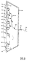
- FIG. 3 shows the antenna (array) arrangement of FIG. 2, indicated by like reference numerals, and further including an antenna housing 60 (e.g., a radome 62 plus a backplane/extrusion 64).
- the housing is shown in FIG. 3 as a simple rectangle; however, the actual radome and backplane can take various forms and shapes.
- the radome 62 is made from a dielectric material, and the backplane/extrusion 64 from a metallic material (such as aluminum).
- the interaction and functionality of the housing is typically not considered, with respect to influences from lightning (corona discharge) and static build-up.
- FIG. 3 shows the general concept for an active antenna system in accordance with the invention.
- active electronic components 66 are shown at various stages of the corporate feed 44; directly after each antenna element 42 (directly at each feed point) and/or at various stages prior to a final input/output connector 68. This arrangement applies to transmit as well as receive antennas, or to antennas used as both transmit/receive antennas.
- the active components 66 can be any discrete device, or a number of discrete devices, IC's or circuits, such as amplifiers (devices or circuits), active phase shifters, RF power detectors, LNAs (Low Noise Amplifiers), etc.
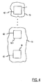
- FIG. 4 shows an example of a plurality of patch/microstrip antenna elements 42, which comprise a typical antenna.
- the configuration shown is a single column of M antenna elements 42, however, this concept readily applies to a general (2-dimensional) M x N array of elements as well.
- These elements are typically etched on a dielectric substrate (or "superstrate”) 70 located above the ground plane 48 containing the apertures 46 (not shown in FIG. 4) such as a floating printed circuit board (PCB) not directly connected to the ground plane 48 (i.e. an air gap between the two boards).
- This substrate 70 may be a PCB (printed circuit board).
- FIG. 5 shows an example of a single patch antenna element 42, one of the elements from FIG. 4, with the polarization of the antenna element indicated as vertical by arrows 55. Therefore, the RF voltage is highest on the top and bottom of the patch 42. The RF voltage is near zero on the symmetry line (center) 45 of the patch, as shown in FIG. 5. In the area directly above and below the symmetry line, the RF voltage is low, and increases to a maximum (at the patch resonant frequency) towards the top and bottom of the patch. However, low frequency energy and DC energy (voltage) is fairly evenly distributed across the whole patch. Therefore, this energy can be tapped off at nearly any point on the patch. It will be apparent that the same considerations would apply for other polarization directions of the patch(es), e.g., horizontal, diagonal, etc.
- FIG. 6 shows an embodiment of the invention, giving one way to accomplish this.
- Metallic striplines (or coaxial lines) 75 are connected at the symmetry area of the patch and serve as static drain lines or taps. This diagram shows taps on both sides of the patch. This construction keeps the RF characteristics balanced, and does not "skew" the radiation pattern to right or left of the patch (in this case, does not rotate the azimuth pattern to one side or the other).
- FIG. 7 shows an example with the static drain lines 75 on one side only, and a wire 80 connected from the bottom right corner of the drain line 75, to ground.
- the ground can be the ground plane 48 with the apertures, or the backplane 64, or the (grounded) outer connector of the connector 52 or outer conductor of the coaxial cable 26 (to the base station).
- FIG. 6 shows a connector or pin 82 on the dielectric substrate or PCB 70 which can be used to effect a similar ground connection.
- FIG. 8 shows a partial side sectional view embodiment, illustrating of the patch antenna system, with lightning protection static drain lines 75, connected to ground.
- the absorbed DC or low frequency energy is directly ported to ground, rather than passing through the antenna (RF) apertures 46, to the stripline (or coaxial) feed lines 44, and then going through the sensitive electronics 66.
- FIG. 9 shows embodiment in a more complete system, in which all internal electronics 66 are now shielded from the lightning, corona, or static (low frequency or DC) energy.
- the (metallic) ground plane 48 (with apertures 46) is directly connected to the (metallic) backplane 64 of the system.
- This backplane 64 is connected to an RF connector 52 for the coaxial cable 26 to the base station.
- the outer shield of the coaxial cable 26 shunts the energy to ground.
- the backplane (or the antenna housing) 64, as well as the patch ground plane 48 are connected with each other and to form a "closed" area defining a Gaussian shield around all internal electronics. This is to ensure that no low frequency RF (at high voltage/power levels) can leak in and damage the sensitive electronics. There should not be any large holes (greater than about 1.2 cm (1 ⁇ 2 inch), anywhere on the outer shield or shell (elements 48 and 64 in the embodiment of FIG. 9) of the system, that can "leak” low frequency or DC energy to the internal electronics. This "shell” further enhances the lightning protection arrangement for the sensitive internal electronic components 66.
- This shield or shell could also be made from metal mesh, with mesh size of less than 1/100th of a wavelength.
Landscapes
- Engineering & Computer Science (AREA)
- Computer Networks & Wireless Communication (AREA)
- Details Of Aerials (AREA)
- Waveguide Aerials (AREA)
- Variable-Direction Aerials And Aerial Arrays (AREA)
- Emergency Protection Circuit Devices (AREA)
Applications Claiming Priority (2)
| Application Number | Priority Date | Filing Date | Title |
|---|---|---|---|
| US09/483,648 US6362787B1 (en) | 1999-04-26 | 2000-01-14 | Lightning protection for an active antenna using patch/microstrip elements |
| US483648 | 2000-01-14 |
Publications (3)
| Publication Number | Publication Date |
|---|---|
| EP1117147A2 EP1117147A2 (en) | 2001-07-18 |
| EP1117147A3 EP1117147A3 (en) | 2003-10-15 |
| EP1117147B1 true EP1117147B1 (en) | 2006-08-09 |
Family
ID=23920936
Family Applications (1)
| Application Number | Title | Priority Date | Filing Date |
|---|---|---|---|
| EP01100096A Expired - Lifetime EP1117147B1 (en) | 2000-01-14 | 2001-01-11 | Lightning protection for an active antenna using patch/microstrip elements |
Country Status (11)
| Country | Link |
|---|---|
| US (1) | US6362787B1 (enExample) |
| EP (1) | EP1117147B1 (enExample) |
| JP (1) | JP2001237634A (enExample) |
| KR (1) | KR20010086337A (enExample) |
| CN (1) | CN1213510C (enExample) |
| AT (1) | ATE336088T1 (enExample) |
| AU (1) | AU777157C (enExample) |
| BR (1) | BR0100069A (enExample) |
| CA (1) | CA2329668C (enExample) |
| DE (1) | DE60122029T2 (enExample) |
| IL (1) | IL140423A (enExample) |
Cited By (1)
| Publication number | Priority date | Publication date | Assignee | Title |
|---|---|---|---|---|
| EP2899802B1 (en) * | 2014-01-15 | 2017-11-01 | Honeywell International Inc. | Anti-lightning combined-stripline-circuit system |
Families Citing this family (13)
| Publication number | Priority date | Publication date | Assignee | Title |
|---|---|---|---|---|
| RU2271813C1 (ru) * | 2004-10-18 | 2006-03-20 | Государственное образовательное учреждение высшего профессионального образования "Нижегородская Государственная Медицинская академия" МЗ РФ (ГОУ ВПО НижГМА) | Способ коррекции морфологического состояния печени опухоленосителя |
| US7576655B2 (en) * | 2005-03-29 | 2009-08-18 | Accu-Sort Systems, Inc. | RFID conveyor system and method |
| TWM294742U (en) * | 2005-10-19 | 2006-07-21 | Lite On Technology Corp | Electrostatic discharge protection receiving system |
| GB2440192B (en) * | 2006-07-17 | 2011-05-04 | Ubidyne Inc | Antenna array system |
| FR2993103B1 (fr) * | 2012-07-05 | 2014-08-15 | Dassault Aviat | Ensemble d'antenne |
| CN103454569A (zh) * | 2013-09-23 | 2013-12-18 | 镇江艾科半导体有限公司 | 半导体芯片测试板 |
| KR101929348B1 (ko) * | 2017-04-21 | 2018-12-14 | 주식회사 감마누 | Pimd 신호 제거가 가능한, 능동소자를 포함하는 기지국 안테나 장치 |
| CN107834199B (zh) * | 2017-12-01 | 2023-06-16 | 成都信息工程大学 | 一种智能主动防雷天线及防雷系统 |
| CN109244654B (zh) * | 2018-08-20 | 2022-09-27 | 中国电力科学研究院有限公司 | 一种电视干扰测量用贴片天线、电视干扰测量装置及方法 |
| CN109728575B (zh) * | 2018-12-21 | 2020-10-23 | 中电科航空电子有限公司 | 一种机载天线防雷电路系统 |
| DE202019101043U1 (de) * | 2019-02-22 | 2020-05-25 | Ericsson Ab | Phasenschiebermodulanordnung zum Einsatz in einer Mobilfunkantenne |
| CN114447583B (zh) * | 2019-08-23 | 2023-09-01 | 华为技术有限公司 | 天线及电子设备 |
| WO2025038381A1 (en) * | 2023-08-11 | 2025-02-20 | Viasat, Inc. | Radiation-induced charge dispersion path |
Family Cites Families (46)
| Publication number | Priority date | Publication date | Assignee | Title |
|---|---|---|---|---|
| US4124852A (en) | 1977-01-24 | 1978-11-07 | Raytheon Company | Phased power switching system for scanning antenna array |
| US4360813A (en) | 1980-03-19 | 1982-11-23 | The Boeing Company | Power combining antenna structure |
| US4566013A (en) | 1983-04-01 | 1986-01-21 | The United States Of America As Represented By The Secretary Of The Navy | Coupled amplifier module feed networks for phased array antennas |
| US4689631A (en) | 1985-05-28 | 1987-08-25 | American Telephone And Telegraph Company, At&T Bell Laboratories | Space amplifier |
| US4825172A (en) | 1987-03-30 | 1989-04-25 | Hughes Aircraft Company | Equal power amplifier system for active phase array antenna and method of arranging same |
| US4849763A (en) | 1987-04-23 | 1989-07-18 | Hughes Aircraft Company | Low sidelobe phased array antenna using identical solid state modules |
| JP2655409B2 (ja) | 1988-01-12 | 1997-09-17 | 日本電気株式会社 | マイクロ波着陸誘導装置 |
| US5412414A (en) | 1988-04-08 | 1995-05-02 | Martin Marietta Corporation | Self monitoring/calibrating phased array radar and an interchangeable, adjustable transmit/receive sub-assembly |
| JPH02308604A (ja) * | 1989-05-23 | 1990-12-21 | Harada Ind Co Ltd | 移動通信用平板アンテナ |
| FR2649544B1 (fr) | 1989-07-04 | 1991-11-29 | Thomson Csf | Systeme d'antenne a faisceaux multiples a modules actifs et formation de faisceaux par le calcul numerique |
| FR2659512B1 (fr) | 1990-03-09 | 1994-04-29 | Cogema | Installation de communication en hyperfrequences. |
| US5513176A (en) | 1990-12-07 | 1996-04-30 | Qualcomm Incorporated | Dual distributed antenna system |
| US5809395A (en) | 1991-01-15 | 1998-09-15 | Rogers Cable Systems Limited | Remote antenna driver for a radio telephony system |
| US5802173A (en) | 1991-01-15 | 1998-09-01 | Rogers Cable Systems Limited | Radiotelephony system |
| EP0501314B1 (en) | 1991-02-28 | 1998-05-20 | Hewlett-Packard Company | Modular distributed antenna system |
| FR2674997B1 (fr) | 1991-04-05 | 1994-10-07 | Alcatel Espace | Architecture de charge utile dans le domaine spatial. |
| JP2735727B2 (ja) * | 1992-01-23 | 1998-04-02 | 三菱電機株式会社 | アレーアンテナ装置 |
| US5280297A (en) | 1992-04-06 | 1994-01-18 | General Electric Co. | Active reflectarray antenna for communication satellite frequency re-use |
| US5627879A (en) | 1992-09-17 | 1997-05-06 | Adc Telecommunications, Inc. | Cellular communications system with centralized base stations and distributed antenna units |
| FR2699008B1 (fr) | 1992-12-04 | 1994-12-30 | Alcatel Espace | Antenne active à synthèse de polarisation variable. |
| US5327150A (en) | 1993-03-03 | 1994-07-05 | Hughes Aircraft Company | Phased array antenna for efficient radiation of microwave and thermal energy |
| EP0647978B1 (en) | 1993-08-12 | 2002-10-23 | Nortel Networks Limited | Base station antenna arrangement |
| GB2281010B (en) | 1993-08-12 | 1998-04-15 | Northern Telecom Ltd | Base station antenna arrangement |
| US5832389A (en) | 1994-03-24 | 1998-11-03 | Ericsson Inc. | Wideband digitization systems and methods for cellular radiotelephones |
| US5724666A (en) | 1994-03-24 | 1998-03-03 | Ericsson Inc. | Polarization diversity phased array cellular base station and associated methods |
| US5548813A (en) | 1994-03-24 | 1996-08-20 | Ericsson Inc. | Phased array cellular base station and associated methods for enhanced power efficiency |
| US5619210A (en) | 1994-04-08 | 1997-04-08 | Ericsson Inc. | Large phased-array communications satellite |
| AU686388B2 (en) | 1994-06-03 | 1998-02-05 | Telefonaktiebolaget Lm Ericsson (Publ) | Microstrip antenna array |
| US5621422A (en) * | 1994-08-22 | 1997-04-15 | Wang-Tripp Corporation | Spiral-mode microstrip (SMM) antennas and associated methods for exciting, extracting and multiplexing the various spiral modes |
| US5710804A (en) | 1995-07-19 | 1998-01-20 | Pcs Solutions, Llc | Service protection enclosure for and method of constructing a remote wireless telecommunication site |
| US5854611A (en) | 1995-07-24 | 1998-12-29 | Lucent Technologies Inc. | Power shared linear amplifier network |
| JPH0964758A (ja) | 1995-08-30 | 1997-03-07 | Matsushita Electric Ind Co Ltd | ディジタル携帯無線機の送信装置とそれに用いる高周波電力増幅装置 |
| US5751250A (en) | 1995-10-13 | 1998-05-12 | Lucent Technologies, Inc. | Low distortion power sharing amplifier network |
| US5604462A (en) | 1995-11-17 | 1997-02-18 | Lucent Technologies Inc. | Intermodulation distortion detection in a power shared amplifier network |
| US5646631A (en) | 1995-12-15 | 1997-07-08 | Lucent Technologies Inc. | Peak power reduction in power sharing amplifier networks |
| SE9603565D0 (sv) * | 1996-05-13 | 1996-09-30 | Allgon Ab | Flat antenna |
| US5862459A (en) | 1996-08-27 | 1999-01-19 | Telefonaktiebolaget Lm Ericsson | Method of and apparatus for filtering intermodulation products in a radiocommunication system |
| WO1998011626A1 (en) | 1996-09-16 | 1998-03-19 | Raytheon Company | Antenna system for enhancing the coverage area, range and reliability of wireless base stations |
| US6072434A (en) * | 1997-02-04 | 2000-06-06 | Lucent Technologies Inc. | Aperture-coupled planar inverted-F antenna |
| US6008750A (en) * | 1997-02-11 | 1999-12-28 | Decatur Electronics, Inc. | Microwave transceiver utilizing a microstrip antenna |
| SE510995C2 (sv) | 1997-03-24 | 1999-07-19 | Ericsson Telefon Ab L M | Aktiv sändnings/mottagnings gruppantenn |
| US6104935A (en) | 1997-05-05 | 2000-08-15 | Nortel Networks Corporation | Down link beam forming architecture for heavily overlapped beam configuration |
| SE509278C2 (sv) | 1997-05-07 | 1999-01-11 | Ericsson Telefon Ab L M | Radioantennanordning och förfarande för samtidig alstring av bred lob och smal peklob |
| NL1006812C2 (nl) | 1997-08-20 | 1999-02-23 | Hollandse Signaalapparaten Bv | Antennesysteem. |
| US5987335A (en) * | 1997-09-24 | 1999-11-16 | Lucent Technologies Inc. | Communication system comprising lightning protection |
| US6140976A (en) | 1999-09-07 | 2000-10-31 | Motorola, Inc. | Method and apparatus for mitigating array antenna performance degradation caused by element failure |
-
2000
- 2000-01-14 US US09/483,648 patent/US6362787B1/en not_active Expired - Fee Related
- 2000-12-19 IL IL140423A patent/IL140423A/en not_active IP Right Cessation
- 2000-12-22 AU AU72505/00A patent/AU777157C/en not_active Ceased
- 2000-12-27 CA CA002329668A patent/CA2329668C/en not_active Expired - Fee Related
-
2001
- 2001-01-10 JP JP2001002369A patent/JP2001237634A/ja active Pending
- 2001-01-11 EP EP01100096A patent/EP1117147B1/en not_active Expired - Lifetime
- 2001-01-11 AT AT01100096T patent/ATE336088T1/de not_active IP Right Cessation
- 2001-01-11 DE DE60122029T patent/DE60122029T2/de not_active Expired - Fee Related
- 2001-01-12 BR BR0100069-1A patent/BR0100069A/pt not_active IP Right Cessation
- 2001-01-13 KR KR1020010002071A patent/KR20010086337A/ko not_active Abandoned
- 2001-01-15 CN CNB011012684A patent/CN1213510C/zh not_active Expired - Fee Related
Cited By (1)
| Publication number | Priority date | Publication date | Assignee | Title |
|---|---|---|---|---|
| EP2899802B1 (en) * | 2014-01-15 | 2017-11-01 | Honeywell International Inc. | Anti-lightning combined-stripline-circuit system |
Also Published As
| Publication number | Publication date |
|---|---|
| IL140423A (en) | 2006-08-20 |
| ATE336088T1 (de) | 2006-09-15 |
| AU777157B2 (en) | 2004-10-07 |
| CN1213510C (zh) | 2005-08-03 |
| AU777157C (en) | 2005-07-21 |
| JP2001237634A (ja) | 2001-08-31 |
| CA2329668C (en) | 2003-08-19 |
| US6362787B1 (en) | 2002-03-26 |
| EP1117147A3 (en) | 2003-10-15 |
| CA2329668A1 (en) | 2001-07-14 |
| AU7250500A (en) | 2001-07-19 |
| DE60122029T2 (de) | 2007-02-22 |
| IL140423A0 (en) | 2002-02-10 |
| CN1306318A (zh) | 2001-08-01 |
| BR0100069A (pt) | 2001-08-21 |
| KR20010086337A (ko) | 2001-09-10 |
| DE60122029D1 (de) | 2006-09-21 |
| EP1117147A2 (en) | 2001-07-18 |
Similar Documents
| Publication | Publication Date | Title |
|---|---|---|
| US4916457A (en) | Printed-circuit crossed-slot antenna | |
| US6292154B1 (en) | Antenna device | |
| US6359588B1 (en) | Patch antenna | |
| EP1117147B1 (en) | Lightning protection for an active antenna using patch/microstrip elements | |
| KR960016369B1 (ko) | 평면안테나 | |
| US20170194703A1 (en) | Antenna array with reduced mutual coupling effect | |
| EP3935689B1 (en) | Antenna structure and method for manufacturing the same | |
| US11005162B2 (en) | Antenna structure of wireless communication device | |
| US12381334B2 (en) | Antenna device, array of antenna devices, and base station with antenna device | |
| US20030112200A1 (en) | Horizontally polarized printed circuit antenna array | |
| AU2020401268B2 (en) | Omnidirectional horizontally polarized antenna with high current protection | |
| CN114600315B (zh) | 双极化天线模块及包括所述天线模块的电子设备 | |
| WO2002023669A1 (en) | A dual polarised antenna | |
| US6765537B1 (en) | Dual uncoupled mode box antenna | |
| WO2021197400A1 (en) | A patch antenna | |
| CN217788794U (zh) | 大扫描角度的天线模组及电子设备 | |
| US11557823B2 (en) | Antenna component | |
| US20250167461A1 (en) | Antenna system with low-pass filter | |
| KR102319004B1 (ko) | 차량용 광대역 평면 역원추 안테나 | |
| CN212366219U (zh) | 指向性天线 | |
| US20250202131A1 (en) | Integrated antenna array with feed and calibration networks | |
| CN115693127A (zh) | 一种宽带圆极化高增益低副瓣定向天线及其天线单元 | |
| CN120637896A (zh) | 一种紧凑型毫米波双极化滤波天线及阵列 |
Legal Events
| Date | Code | Title | Description |
|---|---|---|---|
| PUAI | Public reference made under article 153(3) epc to a published international application that has entered the european phase |
Free format text: ORIGINAL CODE: 0009012 |
|
| AK | Designated contracting states |
Kind code of ref document: A2 Designated state(s): AT BE CH CY DE DK ES FI FR GB GR IE IT LI LU MC NL PT SE TR |
|
| AX | Request for extension of the european patent |
Free format text: AL;LT;LV;MK;RO;SI |
|
| PUAL | Search report despatched |
Free format text: ORIGINAL CODE: 0009013 |
|
| AK | Designated contracting states |
Kind code of ref document: A3 Designated state(s): AT BE CH CY DE DK ES FI FR GB GR IE IT LI LU MC NL PT SE TR |
|
| AX | Request for extension of the european patent |
Extension state: AL LT LV MK RO SI |
|
| RIC1 | Information provided on ipc code assigned before grant |
Ipc: 7H 01Q 21/08 B Ipc: 7H 01Q 1/50 A Ipc: 7H 01Q 1/24 B Ipc: 7H 01Q 9/04 B Ipc: 7H 01Q 23/00 B |
|
| 17P | Request for examination filed |
Effective date: 20040123 |
|
| AKX | Designation fees paid |
Designated state(s): AT BE CH CY DE DK ES FI FR GB GR IE IT LI LU MC NL PT SE TR |
|
| 17Q | First examination report despatched |
Effective date: 20040706 |
|
| GRAP | Despatch of communication of intention to grant a patent |
Free format text: ORIGINAL CODE: EPIDOSNIGR1 |
|
| GRAS | Grant fee paid |
Free format text: ORIGINAL CODE: EPIDOSNIGR3 |
|
| GRAA | (expected) grant |
Free format text: ORIGINAL CODE: 0009210 |
|
| AK | Designated contracting states |
Kind code of ref document: B1 Designated state(s): AT BE CH CY DE DK ES FI FR GB GR IE IT LI LU MC NL PT SE TR |
|
| PG25 | Lapsed in a contracting state [announced via postgrant information from national office to epo] |
Ref country code: BE Free format text: LAPSE BECAUSE OF FAILURE TO SUBMIT A TRANSLATION OF THE DESCRIPTION OR TO PAY THE FEE WITHIN THE PRESCRIBED TIME-LIMIT Effective date: 20060809 Ref country code: NL Free format text: LAPSE BECAUSE OF FAILURE TO SUBMIT A TRANSLATION OF THE DESCRIPTION OR TO PAY THE FEE WITHIN THE PRESCRIBED TIME-LIMIT Effective date: 20060809 Ref country code: AT Free format text: LAPSE BECAUSE OF FAILURE TO SUBMIT A TRANSLATION OF THE DESCRIPTION OR TO PAY THE FEE WITHIN THE PRESCRIBED TIME-LIMIT Effective date: 20060809 Ref country code: IT Free format text: LAPSE BECAUSE OF FAILURE TO SUBMIT A TRANSLATION OF THE DESCRIPTION OR TO PAY THE FEE WITHIN THE PRESCRIBED TIME-LIMIT;WARNING: LAPSES OF ITALIAN PATENTS WITH EFFECTIVE DATE BEFORE 2007 MAY HAVE OCCURRED AT ANY TIME BEFORE 2007. THE CORRECT EFFECTIVE DATE MAY BE DIFFERENT FROM THE ONE RECORDED. Effective date: 20060809 |
|
| REG | Reference to a national code |
Ref country code: GB Ref legal event code: FG4D |
|
| REG | Reference to a national code |
Ref country code: CH Ref legal event code: EP |
|
| REG | Reference to a national code |
Ref country code: IE Ref legal event code: FG4D |
|
| REF | Corresponds to: |
Ref document number: 60122029 Country of ref document: DE Date of ref document: 20060921 Kind code of ref document: P |
|
| REG | Reference to a national code |
Ref country code: CH Ref legal event code: NV Representative=s name: NOVAGRAAF INTERNATIONAL SA Ref country code: SE Ref legal event code: TRGR |
|
| PG25 | Lapsed in a contracting state [announced via postgrant information from national office to epo] |
Ref country code: DK Free format text: LAPSE BECAUSE OF FAILURE TO SUBMIT A TRANSLATION OF THE DESCRIPTION OR TO PAY THE FEE WITHIN THE PRESCRIBED TIME-LIMIT Effective date: 20061109 |
|
| PG25 | Lapsed in a contracting state [announced via postgrant information from national office to epo] |
Ref country code: ES Free format text: LAPSE BECAUSE OF FAILURE TO SUBMIT A TRANSLATION OF THE DESCRIPTION OR TO PAY THE FEE WITHIN THE PRESCRIBED TIME-LIMIT Effective date: 20061120 |
|
| PG25 | Lapsed in a contracting state [announced via postgrant information from national office to epo] |
Ref country code: PT Free format text: LAPSE BECAUSE OF FAILURE TO SUBMIT A TRANSLATION OF THE DESCRIPTION OR TO PAY THE FEE WITHIN THE PRESCRIBED TIME-LIMIT Effective date: 20070109 |
|
| PG25 | Lapsed in a contracting state [announced via postgrant information from national office to epo] |
Ref country code: IE Free format text: LAPSE BECAUSE OF NON-PAYMENT OF DUE FEES Effective date: 20070111 |
|
| PG25 | Lapsed in a contracting state [announced via postgrant information from national office to epo] |
Ref country code: MC Free format text: LAPSE BECAUSE OF NON-PAYMENT OF DUE FEES Effective date: 20070131 |
|
| NLV1 | Nl: lapsed or annulled due to failure to fulfill the requirements of art. 29p and 29m of the patents act | ||
| ET | Fr: translation filed | ||
| PLBE | No opposition filed within time limit |
Free format text: ORIGINAL CODE: 0009261 |
|
| STAA | Information on the status of an ep patent application or granted ep patent |
Free format text: STATUS: NO OPPOSITION FILED WITHIN TIME LIMIT |
|
| 26N | No opposition filed |
Effective date: 20070510 |
|
| PG25 | Lapsed in a contracting state [announced via postgrant information from national office to epo] |
Ref country code: GR Free format text: LAPSE BECAUSE OF FAILURE TO SUBMIT A TRANSLATION OF THE DESCRIPTION OR TO PAY THE FEE WITHIN THE PRESCRIBED TIME-LIMIT Effective date: 20061110 |
|
| PGFP | Annual fee paid to national office [announced via postgrant information from national office to epo] |
Ref country code: DE Payment date: 20090108 Year of fee payment: 9 Ref country code: FI Payment date: 20090114 Year of fee payment: 9 |
|
| PGFP | Annual fee paid to national office [announced via postgrant information from national office to epo] |
Ref country code: CH Payment date: 20090114 Year of fee payment: 9 Ref country code: GB Payment date: 20090107 Year of fee payment: 9 |
|
| PG25 | Lapsed in a contracting state [announced via postgrant information from national office to epo] |
Ref country code: CY Free format text: LAPSE BECAUSE OF FAILURE TO SUBMIT A TRANSLATION OF THE DESCRIPTION OR TO PAY THE FEE WITHIN THE PRESCRIBED TIME-LIMIT Effective date: 20060809 Ref country code: LU Free format text: LAPSE BECAUSE OF NON-PAYMENT OF DUE FEES Effective date: 20070111 |
|
| PGFP | Annual fee paid to national office [announced via postgrant information from national office to epo] |
Ref country code: IT Payment date: 20090130 Year of fee payment: 9 Ref country code: SE Payment date: 20090108 Year of fee payment: 9 |
|
| PG25 | Lapsed in a contracting state [announced via postgrant information from national office to epo] |
Ref country code: TR Free format text: LAPSE BECAUSE OF FAILURE TO SUBMIT A TRANSLATION OF THE DESCRIPTION OR TO PAY THE FEE WITHIN THE PRESCRIBED TIME-LIMIT Effective date: 20060809 |
|
| PGFP | Annual fee paid to national office [announced via postgrant information from national office to epo] |
Ref country code: FR Payment date: 20090113 Year of fee payment: 9 |
|
| REG | Reference to a national code |
Ref country code: CH Ref legal event code: PL |
|
| GBPC | Gb: european patent ceased through non-payment of renewal fee |
Effective date: 20100111 |
|
| EUG | Se: european patent has lapsed | ||
| REG | Reference to a national code |
Ref country code: FR Ref legal event code: ST Effective date: 20100930 |
|
| PG25 | Lapsed in a contracting state [announced via postgrant information from national office to epo] |
Ref country code: FR Free format text: LAPSE BECAUSE OF NON-PAYMENT OF DUE FEES Effective date: 20100201 Ref country code: LI Free format text: LAPSE BECAUSE OF NON-PAYMENT OF DUE FEES Effective date: 20100131 Ref country code: CH Free format text: LAPSE BECAUSE OF NON-PAYMENT OF DUE FEES Effective date: 20100131 |
|
| PG25 | Lapsed in a contracting state [announced via postgrant information from national office to epo] |
Ref country code: DE Free format text: LAPSE BECAUSE OF NON-PAYMENT OF DUE FEES Effective date: 20100803 Ref country code: FI Free format text: LAPSE BECAUSE OF NON-PAYMENT OF DUE FEES Effective date: 20100111 |
|
| PG25 | Lapsed in a contracting state [announced via postgrant information from national office to epo] |
Ref country code: GB Free format text: LAPSE BECAUSE OF NON-PAYMENT OF DUE FEES Effective date: 20100111 |
|
| PG25 | Lapsed in a contracting state [announced via postgrant information from national office to epo] |
Ref country code: IT Free format text: LAPSE BECAUSE OF NON-PAYMENT OF DUE FEES Effective date: 20100111 |
|
| PG25 | Lapsed in a contracting state [announced via postgrant information from national office to epo] |
Ref country code: SE Free format text: LAPSE BECAUSE OF NON-PAYMENT OF DUE FEES Effective date: 20100112 |