EP1117086A2 - Display apparatus in which blanking data is written during blanking period - Google Patents
Display apparatus in which blanking data is written during blanking period Download PDFInfo
- Publication number
- EP1117086A2 EP1117086A2 EP01100603A EP01100603A EP1117086A2 EP 1117086 A2 EP1117086 A2 EP 1117086A2 EP 01100603 A EP01100603 A EP 01100603A EP 01100603 A EP01100603 A EP 01100603A EP 1117086 A2 EP1117086 A2 EP 1117086A2
- Authority
- EP
- European Patent Office
- Prior art keywords
- blanking
- period
- display
- pixel rows
- region
- Prior art date
- Legal status (The legal status is an assumption and is not a legal conclusion. Google has not performed a legal analysis and makes no representation as to the accuracy of the status listed.)
- Withdrawn
Links
- 238000000034 method Methods 0.000 claims description 17
- 239000004973 liquid crystal related substance Substances 0.000 description 24
- 101100317222 Borrelia hermsii vsp3 gene Proteins 0.000 description 4
- 230000006870 function Effects 0.000 description 4
- 230000004044 response Effects 0.000 description 4
- 101150100956 VSP2 gene Proteins 0.000 description 2
- 238000010586 diagram Methods 0.000 description 2
- 229910021420 polycrystalline silicon Inorganic materials 0.000 description 2
- 229920005591 polysilicon Polymers 0.000 description 2
- 229910021417 amorphous silicon Inorganic materials 0.000 description 1
- 230000003247 decreasing effect Effects 0.000 description 1
- 239000007788 liquid Substances 0.000 description 1
- 238000004519 manufacturing process Methods 0.000 description 1
- 239000011159 matrix material Substances 0.000 description 1
Images


Classifications
-
- G—PHYSICS
- G09—EDUCATION; CRYPTOGRAPHY; DISPLAY; ADVERTISING; SEALS
- G09G—ARRANGEMENTS OR CIRCUITS FOR CONTROL OF INDICATING DEVICES USING STATIC MEANS TO PRESENT VARIABLE INFORMATION
- G09G3/00—Control arrangements or circuits, of interest only in connection with visual indicators other than cathode-ray tubes
- G09G3/20—Control arrangements or circuits, of interest only in connection with visual indicators other than cathode-ray tubes for presentation of an assembly of a number of characters, e.g. a page, by composing the assembly by combination of individual elements arranged in a matrix no fixed position being assigned to or needed to be assigned to the individual characters or partial characters
-
- G—PHYSICS
- G09—EDUCATION; CRYPTOGRAPHY; DISPLAY; ADVERTISING; SEALS
- G09G—ARRANGEMENTS OR CIRCUITS FOR CONTROL OF INDICATING DEVICES USING STATIC MEANS TO PRESENT VARIABLE INFORMATION
- G09G2310/00—Command of the display device
- G09G2310/02—Addressing, scanning or driving the display screen or processing steps related thereto
- G09G2310/0202—Addressing of scan or signal lines
- G09G2310/0205—Simultaneous scanning of several lines in flat panels
-
- G—PHYSICS
- G09—EDUCATION; CRYPTOGRAPHY; DISPLAY; ADVERTISING; SEALS
- G09G—ARRANGEMENTS OR CIRCUITS FOR CONTROL OF INDICATING DEVICES USING STATIC MEANS TO PRESENT VARIABLE INFORMATION
- G09G2310/00—Command of the display device
- G09G2310/02—Addressing, scanning or driving the display screen or processing steps related thereto
- G09G2310/0232—Special driving of display border areas
-
- G—PHYSICS
- G09—EDUCATION; CRYPTOGRAPHY; DISPLAY; ADVERTISING; SEALS
- G09G—ARRANGEMENTS OR CIRCUITS FOR CONTROL OF INDICATING DEVICES USING STATIC MEANS TO PRESENT VARIABLE INFORMATION
- G09G2310/00—Command of the display device
- G09G2310/02—Addressing, scanning or driving the display screen or processing steps related thereto
- G09G2310/0264—Details of driving circuits
- G09G2310/0267—Details of drivers for scan electrodes, other than drivers for liquid crystal, plasma or OLED displays
-
- G—PHYSICS
- G09—EDUCATION; CRYPTOGRAPHY; DISPLAY; ADVERTISING; SEALS
- G09G—ARRANGEMENTS OR CIRCUITS FOR CONTROL OF INDICATING DEVICES USING STATIC MEANS TO PRESENT VARIABLE INFORMATION
- G09G2310/00—Command of the display device
- G09G2310/08—Details of timing specific for flat panels, other than clock recovery
-
- G—PHYSICS
- G09—EDUCATION; CRYPTOGRAPHY; DISPLAY; ADVERTISING; SEALS
- G09G—ARRANGEMENTS OR CIRCUITS FOR CONTROL OF INDICATING DEVICES USING STATIC MEANS TO PRESENT VARIABLE INFORMATION
- G09G3/00—Control arrangements or circuits, of interest only in connection with visual indicators other than cathode-ray tubes
- G09G3/20—Control arrangements or circuits, of interest only in connection with visual indicators other than cathode-ray tubes for presentation of an assembly of a number of characters, e.g. a page, by composing the assembly by combination of individual elements arranged in a matrix no fixed position being assigned to or needed to be assigned to the individual characters or partial characters
- G09G3/34—Control arrangements or circuits, of interest only in connection with visual indicators other than cathode-ray tubes for presentation of an assembly of a number of characters, e.g. a page, by composing the assembly by combination of individual elements arranged in a matrix no fixed position being assigned to or needed to be assigned to the individual characters or partial characters by control of light from an independent source
- G09G3/36—Control arrangements or circuits, of interest only in connection with visual indicators other than cathode-ray tubes for presentation of an assembly of a number of characters, e.g. a page, by composing the assembly by combination of individual elements arranged in a matrix no fixed position being assigned to or needed to be assigned to the individual characters or partial characters by control of light from an independent source using liquid crystals
- G09G3/3611—Control of matrices with row and column drivers
- G09G3/3674—Details of drivers for scan electrodes
- G09G3/3677—Details of drivers for scan electrodes suitable for active matrices only
Definitions
- the present invention relates to a display apparatus, and more particularly, to a display apparatus, which can form black blanks at the upper and lower regions of a display screen.
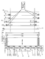
- first row selection pulses corresponding to a half of the pixel rows in the upper blanking region may be sequentially supplied to and shifted in the first group and outputted to the display section at a time.
- second row selection pulses corresponding to a half of the pixel rows in the lower blanking region may be sequentially supplied to and shifted in the third group and outputted to the display section at a time.
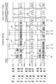
- the first clock signal VCK1 serves as a lock pulse during every horizontal cycle during the video display period. If no data is held in the first shift register group 1, the supply of the first clock signal VCK1 may be stopped. As the operation goes from the state step S1 to the state step S2 during the blanking period, a high-speed clock signal 62 is supplied to the first shift register group 1 as the signal VCK1 so that 30 gate pulses 52 or 30 gate pulses 53 mentioned above are outputted. In the state steps S2 and S3, the first clock signal VCK1 functions as a clock signal 63 having the same duration as in the video display period so that the blanking data can be written into the display panel 7. The clock signal 63 may be either shorter or longer than the horizontal cycle.
Landscapes
- Engineering & Computer Science (AREA)
- Physics & Mathematics (AREA)
- Computer Hardware Design (AREA)
- General Physics & Mathematics (AREA)
- Theoretical Computer Science (AREA)
- Liquid Crystal Display Device Control (AREA)
- Control Of Indicators Other Than Cathode Ray Tubes (AREA)
- Control Of El Displays (AREA)
- Details Of Television Scanning (AREA)
Abstract
Description
Claims (16)
- A display apparatus comprising:a display section having pixel rows; andshift registers which drive said pixel rows,wherein said pixel rows are classified into an upper blanking region, a vide display region and a lower blanking region, and a scanning period is classified into a vide display period and a blanking period,said shift registers are grouped into first to third groups such that said first to third groups are independently controlled,wherein said first and third groups are subjected to shifting operations for said upper and lower regions during said blanking period, respectively,said first and third groups drives said display section such that blanking data is written into said upper and lower blanking regions during said blanking period, and said second group drives said display section such that video data is written into said video display region during said vide display period.
- The display apparatus according to claim 1, wherein said first group drives said display section such that said blanking data is written into said upper blanking region during a first portion of said blanking period, and
said third group drives said display section such that said blanking data is written into said lower blanking region during a second portion of said blanking period. - The display apparatus according to claim 2, wherein said first group drives said display section such that said blanking data is written into odd-numbered ones of said pixel rows corresponding to said upper blanking region at a time and then even-numbered ones of said pixel rows corresponding to said upper blanking region at a time during said first portion of said blanking period, and
said second group drives said display section such that said blanking data is written into odd-numbered ones of said pixel rows corresponding to said lower blanking region at a time and then even-numbered ones of said pixel rows corresponding to said lower blanking region at a time during said second portion of said blanking period. - The display apparatus according to claim 3, wherein first row selection pulses corresponding to a half of said pixel rows in said upper blanking region are sequentially supplied to and shifted in said first group and outputted to said display section at a time, and
second row selection pulses corresponding to a half of said pixel rows in said lower blanking region are sequentially supplied to and shifted in said third group and outputted to said display section at a time. - The display apparatus according to claim 4, wherein said first row selection pulses are ejected from said first group after the output to said display section, and
said second row selection pulses are ejected from said third group after the output to said display section. - The display apparatus according to claim 5, wherein a third row selection pulse is supplied to said first group and shifted for said pixel rows in said upper blanking region, during said blanking period, and is used to drive a start one of said pixel rows in said video display region during said vide display period.
- The display apparatus according to any of claims 1 to 6, wherein each of said shift registers can sequentially drive corresponding ones of said pixel rows during a horizontal display period.
- A blanking method in a display apparatus including a display section with pixel rows, wherein said pixel rows are classified into an upper blanking region, a vide display region and a lower blanking region, and a scanning period is classified into a vide display period and a blanking period, said method comprising:(a) driving said display section such that blanking data is written into said upper blanking region during said blanking period;(b) driving said display section such that said blanking data is written into said lower blanking region during said blanking period; and(c) driving said display section such that video data is written into said video display region during said vide display period.
- The blanking method according to claim 8, wherein said (a) driving includes:(d) driving said display section such that said blanking data is written into said upper blanking region during a first portion of said blanking period, and
said (b) driving includes:(e) driving said display section such that said blanking data is written into said lower blanking region during a second portion of said blanking period after said first portion. - The blanking method according to claim 8, wherein said (a) driving includes:(f) driving said display section such that said blanking data is written into odd-numbered ones of said pixel rows corresponding to said upper blanking region at a time; and(g) driving said display section such that said blanking data is written into even-numbered ones of said pixel rows corresponding to said upper blanking region at a time during said first portion of said blanking period after said (f) driving, and
said (b) driving includes:(h) driving said display section such that said blanking data is written into odd-numbered ones of said pixel rows corresponding to said lower blanking region at a time; and(i) driving said display section such that said blanking data is written into even-numbered ones of said pixel rows corresponding to said lower blanking region at a time during said second portion of said blanking period after said (h) driving. - The blanking method according to claim 10, wherein said (f) driving includes:(j) setting first row selection pulses corresponding to a half of said pixel rows in said upper blanking region;(k) outputting said set first row selection pulses to said display section at a time, and
said (g) driving includes:(l) shifting said set first row selection pulses by one pixel row; and(m) outputting said shifted first row selection pulses to said display section at a time. - The blanking method according to claim 10, wherein said (h) driving includes:(n) setting second row selection pulses corresponding to a half of said pixel rows in said lower blanking region;(o) outputting said set first row selection pulses to said display section at a time, and
said (i) driving includes:(p) shifting said set second row selection pulses by one pixel row; and(q) outputting said shifted first row selection pulses to said display section at a time. - The blanking method according to claim 11, wherein said (f) driving includes:
ejecting said first row selection pulses after said (m) outputting. - The blanking method according to claim 12, wherein said (g) driving includes:
ejecting said second row selection pulses after said (q) outputting. - The blanking method according to claim 11, wherein said (f) driving includes:
shifting a third row selection pulse for said pixel rows in said upper blanking region during said blanking period, such that said third row selection pulse is used to drive a start one of said pixel rows in said video display region during said vide display period. - The blanking method according to any of claims 8 to 15, wherein said (c) driving includes:
sequentially driving ones of said pixel rows corresponding to a horizontal display period during the horizontal display period.
Applications Claiming Priority (2)
| Application Number | Priority Date | Filing Date | Title |
|---|---|---|---|
| JP2000003331 | 2000-01-12 | ||
| JP2000003331A JP2001194642A (en) | 2000-01-12 | 2000-01-12 | Blanking device of liquid crystal display, and its blanking method |
Publications (2)
| Publication Number | Publication Date |
|---|---|
| EP1117086A2 true EP1117086A2 (en) | 2001-07-18 |
| EP1117086A3 EP1117086A3 (en) | 2002-09-04 |
Family
ID=18532294
Family Applications (1)
| Application Number | Title | Priority Date | Filing Date |
|---|---|---|---|
| EP01100603A Withdrawn EP1117086A3 (en) | 2000-01-12 | 2001-01-10 | Display apparatus in which blanking data is written during blanking period |
Country Status (4)
| Country | Link |
|---|---|
| US (1) | US20010007448A1 (en) |
| EP (1) | EP1117086A3 (en) |
| JP (1) | JP2001194642A (en) |
| KR (1) | KR100391734B1 (en) |
Cited By (2)
| Publication number | Priority date | Publication date | Assignee | Title |
|---|---|---|---|---|
| EP1758087A4 (en) * | 2004-04-21 | 2008-07-30 | Bridgestone Corp | Information display drive method |
| US7973740B2 (en) | 2004-04-21 | 2011-07-05 | Bridgestone Corporation | Method of driving information display device |
Families Citing this family (9)
| Publication number | Priority date | Publication date | Assignee | Title |
|---|---|---|---|---|
| JP3719974B2 (en) * | 2001-11-26 | 2005-11-24 | 株式会社アドバンスト・ディスプレイ | Liquid crystal drive device |
| CN100384248C (en) * | 2003-06-13 | 2008-04-23 | 钰创科技股份有限公司 | control method and device of liquid crystal display controller |
| JP4551712B2 (en) * | 2004-08-06 | 2010-09-29 | 東芝モバイルディスプレイ株式会社 | Gate line drive circuit |
| US8638280B2 (en) * | 2007-04-27 | 2014-01-28 | Nlt Technologies, Ltd. | Non-rectangular display apparatus |
| KR101630331B1 (en) * | 2009-12-22 | 2016-06-15 | 엘지디스플레이 주식회사 | Driving circuit for liquid crystal display device and method for driving the same |
| JP5798585B2 (en) * | 2013-03-14 | 2015-10-21 | 双葉電子工業株式会社 | Display device, scanning line driving device |
| KR102277714B1 (en) * | 2014-12-31 | 2021-07-15 | 엘지디스플레이 주식회사 | Gate Driver and Display Device having thereof |
| US20160365042A1 (en) * | 2015-06-15 | 2016-12-15 | Apple Inc. | Display Driver Circuitry With Gate Line and Data Line Delay Compensation |
| WO2022082753A1 (en) * | 2020-10-23 | 2022-04-28 | 京东方科技集团股份有限公司 | Display substrate and preparation method therefor, and display apparatus |
Family Cites Families (11)
| Publication number | Priority date | Publication date | Assignee | Title |
|---|---|---|---|---|
| JP2585463B2 (en) * | 1990-10-30 | 1997-02-26 | 株式会社東芝 | Driving method of liquid crystal display device |
| JPH07175454A (en) * | 1993-10-25 | 1995-07-14 | Toshiba Corp | Display control device and display control method |
| JPH07191630A (en) * | 1993-12-27 | 1995-07-28 | Nec Corp | Lcd multisynchronous monitor method |
| JP2625389B2 (en) * | 1994-10-27 | 1997-07-02 | 日本電気株式会社 | Liquid crystal display device and driving method thereof |
| JP2820061B2 (en) * | 1995-03-30 | 1998-11-05 | 日本電気株式会社 | Driving method of liquid crystal display device |
| JP2776313B2 (en) * | 1995-08-23 | 1998-07-16 | 日本電気株式会社 | Liquid crystal display |
| JPH09307839A (en) * | 1996-05-09 | 1997-11-28 | Fujitsu Ltd | Display device, driving method of the display device, and driving circuit |
| JPH10105107A (en) * | 1996-09-30 | 1998-04-24 | Toshiba Corp | Flat panel display |
| KR100234720B1 (en) * | 1997-04-07 | 1999-12-15 | 김영환 | Driving circuit of tft-lcd |
| KR100317823B1 (en) * | 1998-09-24 | 2001-12-24 | 니시무로 타이죠 | A plane display device, an array substrate, and a method for driving the plane display device |
| JP2001154639A (en) * | 1999-11-25 | 2001-06-08 | Nec Viewtechnology Ltd | Liquid crystal display device and driving method therefor |
-
2000
- 2000-01-12 JP JP2000003331A patent/JP2001194642A/en active Pending
-
2001
- 2001-01-08 US US09/755,165 patent/US20010007448A1/en not_active Abandoned
- 2001-01-10 EP EP01100603A patent/EP1117086A3/en not_active Withdrawn
- 2001-01-12 KR KR10-2001-0001720A patent/KR100391734B1/en not_active Expired - Fee Related
Cited By (2)
| Publication number | Priority date | Publication date | Assignee | Title |
|---|---|---|---|---|
| EP1758087A4 (en) * | 2004-04-21 | 2008-07-30 | Bridgestone Corp | Information display drive method |
| US7973740B2 (en) | 2004-04-21 | 2011-07-05 | Bridgestone Corporation | Method of driving information display device |
Also Published As
| Publication number | Publication date |
|---|---|
| KR20010070517A (en) | 2001-07-25 |
| KR100391734B1 (en) | 2003-07-16 |
| US20010007448A1 (en) | 2001-07-12 |
| EP1117086A3 (en) | 2002-09-04 |
| JP2001194642A (en) | 2001-07-19 |
Similar Documents
| Publication | Publication Date | Title |
|---|---|---|
| US6380919B1 (en) | Electro-optical devices | |
| KR100493216B1 (en) | Circuit for driving image signal and display device having the same | |
| US6236388B1 (en) | Image display system for displaying images of different resolutions | |
| US6323871B1 (en) | Display device and its driving method | |
| US12482390B2 (en) | Method of driving display, and display device | |
| US5745093A (en) | Liquid crystal display driving system | |
| US20030090614A1 (en) | Liquid crystal display | |
| US20010015714A1 (en) | Active matrix display and image forming system | |
| US20040041769A1 (en) | Display apparatus | |
| KR100954011B1 (en) | Display device | |
| EP2455932A1 (en) | Display device and display device driving method | |
| JP3353921B2 (en) | Solid-state imaging device | |
| US20040075631A1 (en) | Liquid crystal display | |
| JPH08123367A (en) | Device and method for processing image signal | |
| EP1117086A2 (en) | Display apparatus in which blanking data is written during blanking period | |
| US6271821B1 (en) | Interface for liquid crystal display | |
| US20060007083A1 (en) | Display panel and driving method thereof | |
| JPH0854601A (en) | Active matrix liquid crystal display device | |
| JPH05188885A (en) | Liquid crystal display drive circuit | |
| KR19980071743A (en) | Liquid crystal display | |
| JP3015544B2 (en) | Liquid crystal display | |
| JP3230408B2 (en) | Display device | |
| US20040257349A1 (en) | Display apparatus | |
| KR101075250B1 (en) | Delay time correction circuit video data processing circuit and flat display apparatus | |
| EP0428324A2 (en) | Matrix addressable display and driver having CRT compatibility |
Legal Events
| Date | Code | Title | Description |
|---|---|---|---|
| PUAI | Public reference made under article 153(3) epc to a published international application that has entered the european phase |
Free format text: ORIGINAL CODE: 0009012 |
|
| AK | Designated contracting states |
Kind code of ref document: A2 Designated state(s): AT BE CH CY DE DK ES FI FR GB GR IE IT LI LU MC NL PT SE TR |
|
| AX | Request for extension of the european patent |
Free format text: AL;LT;LV;MK;RO;SI |
|
| PUAL | Search report despatched |
Free format text: ORIGINAL CODE: 0009013 |
|
| AK | Designated contracting states |
Kind code of ref document: A3 Designated state(s): AT BE CH CY DE DK ES FI FR GB GR IE IT LI LU MC NL PT SE TR |
|
| AX | Request for extension of the european patent |
Free format text: AL;LT;LV;MK;RO;SI |
|
| RIC1 | Information provided on ipc code assigned before grant |
Free format text: 7G 09G 3/36 A, 7G 09G 3/28 B |
|
| 17P | Request for examination filed |
Effective date: 20020905 |
|
| 17Q | First examination report despatched |
Effective date: 20021021 |
|
| GRAH | Despatch of communication of intention to grant a patent |
Free format text: ORIGINAL CODE: EPIDOS IGRA |
|
| AKX | Designation fees paid |
Designated state(s): DE FR GB NL |
|
| STAA | Information on the status of an ep patent application or granted ep patent |
Free format text: STATUS: THE APPLICATION HAS BEEN WITHDRAWN |
|
| 18W | Application withdrawn |
Effective date: 20030627 |