EP1114885A1 - CZ SINGLE CRYSTAL DOPED WITH Ga AND WAFER AND METHOD FOR PRODUCTION THEREOF - Google Patents
CZ SINGLE CRYSTAL DOPED WITH Ga AND WAFER AND METHOD FOR PRODUCTION THEREOF Download PDFInfo
- Publication number
- EP1114885A1 EP1114885A1 EP00922915A EP00922915A EP1114885A1 EP 1114885 A1 EP1114885 A1 EP 1114885A1 EP 00922915 A EP00922915 A EP 00922915A EP 00922915 A EP00922915 A EP 00922915A EP 1114885 A1 EP1114885 A1 EP 1114885A1
- Authority
- EP
- European Patent Office
- Prior art keywords
- single crystal
- silicon single
- solar cell
- silicon
- wafer
- Prior art date
- Legal status (The legal status is an assumption and is not a legal conclusion. Google has not performed a legal analysis and makes no representation as to the accuracy of the status listed.)
- Granted
Links
Images



Classifications
-
- C—CHEMISTRY; METALLURGY
- C30—CRYSTAL GROWTH
- C30B—SINGLE-CRYSTAL GROWTH; UNIDIRECTIONAL SOLIDIFICATION OF EUTECTIC MATERIAL OR UNIDIRECTIONAL DEMIXING OF EUTECTOID MATERIAL; REFINING BY ZONE-MELTING OF MATERIAL; PRODUCTION OF A HOMOGENEOUS POLYCRYSTALLINE MATERIAL WITH DEFINED STRUCTURE; SINGLE CRYSTALS OR HOMOGENEOUS POLYCRYSTALLINE MATERIAL WITH DEFINED STRUCTURE; AFTER-TREATMENT OF SINGLE CRYSTALS OR A HOMOGENEOUS POLYCRYSTALLINE MATERIAL WITH DEFINED STRUCTURE; APPARATUS THEREFOR
- C30B15/00—Single-crystal growth by pulling from a melt, e.g. Czochralski method
- C30B15/02—Single-crystal growth by pulling from a melt, e.g. Czochralski method adding crystallising materials or reactants forming it in situ to the melt
- C30B15/04—Single-crystal growth by pulling from a melt, e.g. Czochralski method adding crystallising materials or reactants forming it in situ to the melt adding doping materials, e.g. for n-p-junction
-
- C—CHEMISTRY; METALLURGY
- C30—CRYSTAL GROWTH
- C30B—SINGLE-CRYSTAL GROWTH; UNIDIRECTIONAL SOLIDIFICATION OF EUTECTIC MATERIAL OR UNIDIRECTIONAL DEMIXING OF EUTECTOID MATERIAL; REFINING BY ZONE-MELTING OF MATERIAL; PRODUCTION OF A HOMOGENEOUS POLYCRYSTALLINE MATERIAL WITH DEFINED STRUCTURE; SINGLE CRYSTALS OR HOMOGENEOUS POLYCRYSTALLINE MATERIAL WITH DEFINED STRUCTURE; AFTER-TREATMENT OF SINGLE CRYSTALS OR A HOMOGENEOUS POLYCRYSTALLINE MATERIAL WITH DEFINED STRUCTURE; APPARATUS THEREFOR
- C30B29/00—Single crystals or homogeneous polycrystalline material with defined structure characterised by the material or by their shape
- C30B29/02—Elements
- C30B29/06—Silicon
-
- C—CHEMISTRY; METALLURGY
- C30—CRYSTAL GROWTH
- C30B—SINGLE-CRYSTAL GROWTH; UNIDIRECTIONAL SOLIDIFICATION OF EUTECTIC MATERIAL OR UNIDIRECTIONAL DEMIXING OF EUTECTOID MATERIAL; REFINING BY ZONE-MELTING OF MATERIAL; PRODUCTION OF A HOMOGENEOUS POLYCRYSTALLINE MATERIAL WITH DEFINED STRUCTURE; SINGLE CRYSTALS OR HOMOGENEOUS POLYCRYSTALLINE MATERIAL WITH DEFINED STRUCTURE; AFTER-TREATMENT OF SINGLE CRYSTALS OR A HOMOGENEOUS POLYCRYSTALLINE MATERIAL WITH DEFINED STRUCTURE; APPARATUS THEREFOR
- C30B15/00—Single-crystal growth by pulling from a melt, e.g. Czochralski method
-
- Y—GENERAL TAGGING OF NEW TECHNOLOGICAL DEVELOPMENTS; GENERAL TAGGING OF CROSS-SECTIONAL TECHNOLOGIES SPANNING OVER SEVERAL SECTIONS OF THE IPC; TECHNICAL SUBJECTS COVERED BY FORMER USPC CROSS-REFERENCE ART COLLECTIONS [XRACs] AND DIGESTS
- Y02—TECHNOLOGIES OR APPLICATIONS FOR MITIGATION OR ADAPTATION AGAINST CLIMATE CHANGE
- Y02E—REDUCTION OF GREENHOUSE GAS [GHG] EMISSIONS, RELATED TO ENERGY GENERATION, TRANSMISSION OR DISTRIBUTION
- Y02E10/00—Energy generation through renewable energy sources
- Y02E10/50—Photovoltaic [PV] energy
- Y02E10/547—Monocrystalline silicon PV cells
Definitions
- the present invention relates to a silicon single crystal produced by Czochralski method (hereinafter occasionally referred to as “Czochralski method”, “CZ method”, or a pulling method), which is especially useful for material of solar cell, a method for producing it and a silicon single crystal solar cell produced using it.
- Czochralski method hereinafter occasionally referred to as "Czochralski method”, “CZ method”, or a pulling method
- the solar cell can be roughly classified on the basis of material of the substrate, into three types of silicon crystal solar cell, amorphous silicon solar cell, and compound semiconductor solar cell.
- the silicon crystal solar cell can be further classified into single crystal solar cell and polycrystal solar cell.
- the solar cell having the highest conversion efficiency that is the most important characteristics as a solar cell is the compound semiconductor solar cell among them, of which conversion efficiency is almost 25 %.
- Conversion efficiency means "the rate of energy that can be taken out by being converted to electric energy with a solar cell", that is represented as a percentage (%).
- the solar cell having the highest conversion efficiency except the compound semiconductor solar cell is silicon single crystal solar cell, of which power generation efficiency is about 20 % that is close to conversion efficiency of the compound semiconductor solar cell.
- the substrate for the silicon crystal solar cell can be prepared relatively easily. Accordingly, it is a major type of solar cell used generally. Furthermore, silicon polycrystal solar cell and amorphous silicon solar cell or the like have also been used practically, since the material of the substrate for them can be produced at low cost, although conversion efficiency of them is about 5 to 15 %, which is lower than that of the above-mentioned two types of solar cell.
- a columnar silicon single crystal ingot is produced according to Czochralski method or a floating zone melting method (hereinafter occasionally referred to as FZ method, Floating zone method). Then the ingot is sliced to give a thin wafer having a thickness of, for example about 300 ⁇ m, and a mechanical damage on the surface of the wafer is removed by etching with chemical to provide a wafer (substrate) that is to be a solar cell.
- PN junction is formed on one side of the wafer by a diffusion treatment of impurity (dopant), and thereafter electrode is formed on both surface of the wafer, and finally an antireflection coating film is formed on the surface which gets sunbeam in order to reduce loss of optical energy due to reflection of light, and thereby a solar cell is produced.
- CZ method is suitable for producing a silicon wafer with a large diameter which can be substrate materials for production of a solar cell having wider area, since a silicon single crystal having a large diameter can be easily produced according to CZ method, and the produced silicon single crystal is excellent in strength. Accordingly, a silicon single crystal for a solar cell is mainly produced according to CZ method.
- a silicon wafer can be used as material for substrate of single crystal solar cell, only where its substrate lifetime (hereinafter occasionally referred to as lifetime, LT), that is one of characteristics thereof, is more than 10 ⁇ s. Furthermore, the lifetime is preferably 200 ⁇ s or more in order to provide a solar cell having a high conversion efficiency.
- a conductive type of the wafer that is presently used as a solar cell is mainly P type, and the P type wafer is generally doped with boron as a dopant.
- the single crystal ingot that is material for the wafer can be produced according to CZ method (including MCZ (hereinafter occasionally referred to as Magnetic field applied CZ method) or FZ method, production cost in FZ method is higher than in CZ method, and the silicon single crystal having a large diameter is produced more easily according to CZ method as described above. Accordingly, it is presently produced according to CZ method wherein a single crystal having a large diameter can be produced at relatively low cost.
- the present invention has been accomplished to solve the above-mentioned problems, and an object of the present invention is to provide a silicon single crystal and a silicon single crystal wafer for producing a solar cell having very high conversion efficiency of optical energy that is not suffered from photo-degradation, even though it has high oxygen concentration, and also provide a method for producing them.
- the present invention provides a silicon single crystal doped with Gallium wherein resistivity is 5 ⁇ ⁇ cm to 0.1 ⁇ ⁇ cm.
- the present invention also provides a silicon single crystal doped with Ga wherein concentration of Ga in the crystal is 5 x 10 17 atoms/cm 3 to 3 x 10 15 atoms/cm 3 .
- the amount of Gallium contained in the silicon single crystal of the present invention is preferably such an amount that the resistivity is 0.1 ⁇ ⁇ cm or more, more preferably 0.2 ⁇ ⁇ cm or more.
- concentration of Gallium is preferably 5 x 10 17 atoms/cm 3 or less.
- the lifetime of such a carrier generated in the substrate is called substrate lifetime or lifetime.
- the substrate resistivity gets high, electric power is consumed with internal resistance of the solar cell when it is processed to be a solar cell, so that conversion efficiency may also be lowered.
- the resistivity is 5 ⁇ ⁇ cm or less, more preferably 2.0 ⁇ ⁇ cm or less, or that gallium concentration in the single crystal ingot is 3 x 10 15 atoms/cm 3 or more.
- the present invention also provides a silicon single crystal doped with gallium wherein concentration of interstitial oxygen in the single crystal is 20 x 10 17 atoms/cm 3 (ASTM'79) or less.
- oxygen concentration in the crystal can be as high as that in a general single crystal produced according to CZ method, especially can be high as 20 x 10 17 atoms/cm 3 or less. Accordingly, it is not necessary to make oxygen concentration low forcedly, so that there are advantages that the single crystal can be produced easily, and that strength of the crystal is high since adequate amount of oxygen is contained therein.
- the present invention also provides a silicon single crystal doped with Ga wherein a diameter of the single crystal is 4 inches or more.
- the crystal produced according to CZ method or MCZ method tends to have high oxygen concentration. Accordingly, if a solar cell having high conversion efficiency is to be produced, it has been a general way to produce a single crystal according to FZ method or to produce a single crystal having a small diameter according to MCZ method, in order to achieve low oxygen concentration. However, it is very difficult to produce a single crystal having a diameter of more than 6 inches according to FZ method, and it is also difficult to produce a single crystal having a diameter of more than 4 inches and low oxygen concentration according to MCZ method. Accordingly, it has been considered as inappropriate to produce a single crystal having a large diameter for production of a solar cell having high conversion efficiency.
- a single crystal ingot having a large diameter as 16 inches or 20 inches, which is not used at present can be used as a substrate wafer of a solar cell, so that a solar cell having high conversion efficiency can be easily produced irrespective of the diameter of the single crystal ingot.
- a wafer having a large diameter out of use at present can be used as a substrate of a solar cell, a solar cell itself can be made large, so that it is fully possible to find more use of a solar cell.
- the present invention also provides a silicon single crystal wafer doped with gallium produced by slicing a silicon single crystal doped with gallium produced according to Czochralski method.
- the silicon single crystal wafer doped with gallium is used as a material for a substrate of a solar cell, shortening of the lifetime due to influence of oxygen contained in the crystal can be suppressed. Accordingly, even if the single crystal wafer has high oxygen concentration, a long lifetime that is necessary for a solar cell can be achieved. Thereby, a long lifetime can be achieved even in a cell having a low resistivity, and it has become possible to produce a solar cell wherein a substrate wafer having high oxygen concentration is used, but conversion efficiency is not low, and high performance can be achieved. Furthermore, since oxygen concentration in the wafer is appropriate, there can be achieved an advantage in use that a strength of the wafer is high.
- the resistivity is preferably 5 ⁇ ⁇ cm to 0.1 ⁇ ⁇ cm, and is more preferably 2.0 ⁇ ⁇ cm to 0.2 ⁇ ⁇ cm.
- Ga concentration in the wafer substrate is preferably 5 x 10 17 atoms/cm 3 to 3 x 10 15 atoms/cm 3 , more preferably 1.5 x 10 17 atoms/cm 3 to 7 x 10 15 atoms/cm 3 .
- resistivity of the wafer will be unnecessarily high, and an electric power is consumed with an internal resistance of the solar cell and conversion efficiency may be reduced, when the substrate is processed to be a solar cell. If a resistivity of the wafer is less than 0.1 ⁇ ⁇ cm, or Ga concentration in the wafer is more than 5 x 10 17 atoms/cm 3 , resistivity of substrate will be extremely reduce and, as a result, lifetime of minority carrier will be lowered due to Auger recombination, and conversion efficiency will be lowered.
- Interstitial oxygen concentration in the silicon single crystal wafer doped with Ga of the present invention is preferably 20 x 10 17 atoms/cm 3 (ASTM(79)) or less. Namely, it is acceptable in the case that oxygen concentration in the substrate of the solar cell doped with Ga is as that of a single crystal produced according to CZ method. Namely, a silicon wafer having oxygen concentration of a value incorporated in the crystal during the growth of single crystal, namely a value less than solid solubility of oxygen at a temperature around a melting point of silicon is suitable.
- oxygen concentration of a wafer used for the present invention is preferably 20 x 10 17 atoms/cm 3 or less.
- the silicon single crystal doped with gallium and the silicon single crystal wafer doped with gallium of the present invention is especially useful for a solar cell.
- the silicon single crystal solar cell produced using Ga doped silicon single crystal or Ga doped silicon single crystal wafer is inexpensive and has high energy conversion efficiency.
- Ga doped silicon single crystal ingot grown, for example, by CZ method is processed to be a substrate for a solar cell, and a solar cell is produced using the wafer, a solar cell having stable conversion efficiency can be produced without being affected by concentration of oxygen incorporated in the crystal during the growth of the silicon crystal.
- the Ga doped silicon single crystal is used as material for a solar cell, the substrate lifetime can be stable without being affected by concentration of oxygen, so that there can be produced a solar cell having high conversion efficiency even when resistivity of the solar cell is low.
- the above-mentioned silicon single crystal solar cell can have an area of 100cm 3 or more.
- Ga doped silicon single crystal according to CZ method is used as a substrate for a solar cell, a solar cell having high conversion efficiency, less lowering of conversion efficiency due to photo-degradation and large area can be produced at low production cost, so that cost of solar cell can be further reduced and increase of demand thereon may be expected. Furthermore, if the area is large, more electric current can be obtained from one cell, so that it is also effective for electric power.
- the above-mentioned silicon single crystal solar cell has preferably conversion efficiency of 20 % or more.
- the silicon single crystal solar cell of the present invention can be for space use.
- the silicon single crystal solar cell of the present invention is made of Ga doped single crystal, it is not susceptible to various radiation in space. Namely, rapid photo-degradation as observed in boron dope crystal is not observed. Accordingly, the silicon single crystal solar cell is suitable for space use.
- the silicon single crystal solar cell described above may have a rate of lowering of conversion efficiency due to photo-degradation of 0.5 % or less.
- the silicon single crystal solar cell of the present invention since the silicon single crystal solar cell of the present invention has high conversion efficiency and almost no lowering of conversion efficiency caused by photo-degradation, it is quite effective for a solar cell.
- lowering of conversion efficiency due to photo-degradation represents a value obtained by subtracting conversion efficiency after irradiation of steady-state irradiation with halogen lamp or the like used for solar simulator for 30 hours from conversion efficiency before the irradiation.
- the present invention also provides a method for production of Ga doped silicon single crystal according to CZ method wherein Ga is added in a silicon melt in a crucible, a seed crystal is brought into contact with the silicon melt and is pulled with rotating to grow a silicon single crystal ingot.
- Ga doped silicon single crystal can be produced.
- addition of Ga to a melt in a crucible is preferably conducted by growing a silicon crystal ingot in which Ga of high concentration is added previously, and crashing the silicon single crystal doped with Ga in high concentration to prepare a doping agent, and adding Ga in a silicon melt using it.
- a method of doping Ga in the case that a single crystal in which Ga is added is produced according to the present invention, a method of adding gallium directly to silicon polycrystal before or after being melted can be used, but in the case that the single crystal doped with gallium is mass-produced for industrial purpose, it is preferable that the doping agent is previously prepared to use for doping as described above. If such a method is used, operation can be conducted efficiently. Because, gallium has a low melting point as 30°C, and is difficult to be handled. Accordingly, Ga concentration can be controlled accurately and easily not by adding gallium directly in a crucible, but by preparing a doping agent and doping with it, and an accurate dopant concentration can be achieved. Furthermore, a doping agent is easy to be handled, compared to the case that gallium is directly added in the silicon melt, so that operation efficiency can also be improved.
- the number of rotation of a crucible during growing a Ga doped single crystal ingot can be 30 rpm or less.
- An amount of oxygen eluted from a wall of a crucible can be controlled by changing the number of rotation of the crucible during growing a single crystal, and thereby an amount of oxygen incorporated in the single crystal to be grown can be controlled.
- the upper limit of the number of rotation of the crucible is 30 rpm, in light of ruffle of the liquid surface of the silicon melt or the like generated as a result of the vibration due to rotation of the crucible.
- the single crystal is grown with controlling the number of rotation of the crucible, depending on the intended oxygen concentration of the crystal to be pulled, in the range of 30 rpm or less.
- the upper limit of the number of rotation of the crucible is constant irrespective of the diameter of the single crystal to be pulled or the size of the crucible. Accordingly, if a single crystal is grown with controlling the number of rotation of the crucible in the range of 30 rpm or less, the single crystal can be grown efficiently without causing slip dislocation during the growth of the single crystal.
- a pressure in a furnace of a pulling apparatus during the growth of Ga doped silicon single crystal is in the range of 10 to 500 mbar.
- Oxygen eluted from a wall of a quartz crucible is always evaporated in the form of SiO from a surface of a silicon melt. Accordingly, in order to keep oxygen concentration in the silicon melt at a necessary value, a pressure in a chamber needs to be controlled appropriately. If the pressure in the furnace is 10 mbar or lower, extremely much amount of SiO is evaporated from the silicon melt, and an amount of oxygen eluted from the quartz crucible is increased, resulting in acceleration of degradation of the wall of the quartz crucible, so that the quartz crucible cannot stand against a long period of operation. Therefore, such a low pressure is not preferable.
- the pressure is 500 mbar or more, SiO evaporated from the silicon melt is liable to adhered in the chamber, which may prevent growth of single crystal. Accordingly, unnecessarily high pressure is not preferable. It is preferable to decide a pressure in the furnace selected in the range of 10 to 500 mbar depending on the intended quality of the single crystal ingot to be produced, when Ga doped silicon single crystal ingot is grown.
- An amount of inert gas to be flown in a furnace of a pulling apparatus during growing Ga doped silicon single crystal is preferably in the range of 10 to 500 l/min.
- the amount of inert gas flown above the liquid surface of melt is more than 500 l/min, an amount of SiO removed from the surface of the silicon melt is increased, resulting in acceleration of degradation of the wall of the quartz crucible. Furthermore, if a large amount of inert gas is brought into contact with the surface of the silicon melt, ruffle of the melt is enlarged, resulting in inhibiting growth of the single crystal ingot, which may lead to a problem that a single crystal cannot be pulled.
- an amount of inert gas is less than 10 l/min, effect of removing SiO evaporated from the surface of the melt is lowered, there may be generated problems that cause dislocation generation during growing single crystal, for example, oxides of silicon may be precipitated on the upper part of the crucible.
- an amount of inert gas during growing single crystal is preferably controlled in the range of 10 to 500 l/min depending on intended quality of crystal.
- the inert gas flown in the furnace of the pulling apparatus during growing Ga doped silicon single crystal is argon.
- argon is used as the inert gas flown in the furnace of the pulling apparatus during glowing the single crystal, any degradation of quality as will be problem in the solar cell is not caused, when the single crystal ingot is processed to be the solar cell, so that the substrate wafer having a stable quality can be produced, since Ar is chemically stable and does not affect the quality of the single crystal that is grown.
- the silicon single crystal and silicon single crystal wafer produced by Czochralski method is doped with Ga according to the present invention, photo-degradation is not caused even in the case that the single crystal having high oxygen concentration is produced, so that silicon single crystal and silicon single crystal wafer for producing a solar cell having very high conversion efficiency of optical energy can be produced.
- the present invention facilitates manufacture of these products with a large diameter, sufficient strength of crystal and excellent durability.
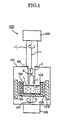
- Fig. 1 is a structural drawing of an example of apparatus for pulling single crystal by CZ method used for the present invention.
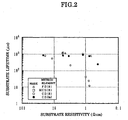
- Fig. 2 is a graph showing a relation between a substrate resistivity and a substrate lifetime.
- Fig. 3 is a graph showing a relation between a substrate resistivity and a substrate lifetime at a low resistivity.
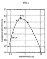
- Fig. 4 is a graph showing a relation between a substrate resistivity and a conversion efficiency of a solar cell produced using the substrate.
- Fig. 5 is a graph showing a relation between a substrate resistivity and conversion efficiency of a solar cell having a large area produced using the substrate.
- Fig.6 is a graph showing a result of DLTS measurement.
- Fig.7 is a graph showing a relation between a dose of electric beam and a rate of decrease of electric current in a solar cell.
- the inventors have studied the condition for obtaining a substrate of a solar cell that can be produced with relative ease and can be mass-produced, and at the same time have a high conversion efficiency as material for a substrate of a solar cell, and made experiments therefor repeatedly and studied further, and have accomplished the present invention.
- the inventors have found that since oxygen and boron exist at the same time in crystal in the solar cell produced using a conventional P type silicon single crystal doped with boron as a dopant produced by CZ method, deep level (also called trap level) due to oxygen and boron is formed in a bulk of the solar cell, and carrier in the solar cell is trapped in the deep level, resulting in shortening of substrate lifetime and photo-degradation, and have noted that the substrate lifetime is shorten only when both oxygen and boron exist at the same time, and the lifetime is not changed and photo-degradation is not caused when only one of oxygen and boron exists, and have completed the present invention.
- deep level also called trap level
- the substrate lifetime is shorten only when both oxygen and boron exist at the same time, and the lifetime is not changed and photo-degradation is not caused when only one of oxygen and boron exists, and have completed the present invention.
- P type silicon single crystal wafer As a substrate of a solar cell, P type silicon single crystal wafer has been mainly used.
- the inventors have considered that if P type silicon single crystal can be produced using other elements than boron, substrate lifetime is not shortened even when oxygen exists in the crystal, and a solar cell wherein less photo-degradation is caused can be produced, and have made experiments repeatedly. Then, they have confirmed that there can be produced a solar cell wherein lifetime is always stable and photo-degradation is not caused even when high concentration of oxygen exists in crystal, by using the substrate produced by pulling P type silicon single crystal with adding gallium as a dopant.
- the wafer resistivity is more than 5 ⁇ ⁇ cm, the resistivity is unnecessarily high, and electric power is consumed by the internal resistance of the solar cell so that conversion efficiency may also be lowered. If the resistivity is less than 0.1 ⁇ ⁇ cm, the substrate resistivity is extremely low, and shortening of lifetime of minority carrier is caused in the substrate due to Auger recombination, resulting in lowering of conversion efficiency of cell as well.
- a wafer having larger diameter than that of a conventional wafer can be used as a substrate. Since a conventional single crystal doped with boron having a large diameter contains high concentration of oxygen, photo-degradation of the substrate of the solar cell is caused. However, if single crystal doped with gallium in an appropriate amount so that a resistivity may be 5 ⁇ ⁇ cm to 0.1 ⁇ ⁇ cm is used, high conversion efficiency can be achieved irrespective of oxygen concentration even in the single crystal substrate having a large diameter, so that a larger solar cell can be developed in future. Furthermore, oxygen is contained in an appropriate amount, strength of the crystal is high, good workability can be achieved, and durability of the resultant solar cell can be improved.
- solar cells are connected in series or in parallel to be modularized so that intended electric power can be output for practical use.
- a lot of solar cells should be connected. Accordingly, a solar cell having larger area is more advantageous in order to achieve simplification of a solar cell module, downsizing, and reduction of production cost. If a solar cell having a large size and high conversion efficiency can be used as material of solar cell module, further reduction in cost of a solar cell and increase of demand thereon can be achieved.
- the silicon single crystal doped with gallium in an adequate amount so that a resistivity may be 5 ⁇ ⁇ cm to 0.1 ⁇ ⁇ cm is used as a substrate of a solar cell, a solar cell wherein lowering of conversion efficiency due to photo-degradation is little and conversion efficiency is high, and silicon single crystal having a large diameter can be produced according to CZ method.
- a large solar cell such as those having an area of 100 cm 2 or more can be mass-produced at low cost.
- the apparatus 100 for pulling single crystal comprises a bottom chamber 101 including a crucible 102 for melting raw material and a top chamber 110 in which a pulled single crystal is put and from which it is taken out.
- a wire winding mechanism 109 for pulling a single crystal, which is operated so that a wire 1 may be wound up and down with growing of single crystal.
- seed crystal S is attached to a seed holder 22 for pulling the silicon single crystal.
- the crucible 102 in the bottom chamber 101 comprises an inner part 103 made of quartz and an outer part 104 made of graphite.
- a heater 105 for melting polycrystal silicon raw material charged in the crucible is disposed around the crucible 102.
- a heat insulating material 106 is disposed around the heater 105.
- the crucible 102 is filled with silicon melt L melted by heating with the heater.
- the crucible is supported with a supporting shaft 107 for rotating and moving vertically the crucible 102 and a driving apparatus 108 therefor is attached at a lower part of the bottom chamber.
- a gas flow-guide cylinder 2 can also be provided in order to straighten an inert gas introduced in the furnace.
- the seed crystal S for growing a single crystal ingot is attached at the end of the wire 1 of the pulling apparatus, and the wire 1 is winding down quietly so that the tip end of the seed crystal may be brought into contact with the silicon melt L.
- the crucible 102 and the seed crystal S rotate to a different direction from each other.
- Space in the pulling apparatus is under a reduced pressure, and is filled with inert gas such as argon or the like flown from the upper part of the furnace.
- the wire 1 is wound up quietly with rotating the seed crystal S and the crucible 102 to a different direction from each other, and thereby pulling of the seed crystal is initiated. Then, necking operation is initiated in order to eliminate slip dislocation generated in the seed crystal. When the necking operation is continued to the thickness or length at which slip dislocation is eliminated, pulling is conducted so that the diameter of the crystal may get large gradually to form a cone part of the single crystal, with increasing the diameter to a desired value. When the diameter of the cone part becomes a predetermined value, formation of a constant diameter part (a body) of the single crystal ingot is initiated.
- a rotation rate of the crucible, a pulling rate, inert gas pressure in the chamber, a flow amount or the like in that time are controlled appropriately depending on oxygen concentration in the single crystal to be grown.
- the diameter of the crystal can be controlled by adjusting the temperature and the pulling rate.
- a tail part is formed by decreasing a diameter of the crystal, and then the tip end of the tail is cut off from the surface of the silicon melt, and the grown silicon single crystal is lifted to the top chamber 110 by winding up the wire, and allowed to be cooled.
- the single crystal ingot is cooled so that it may be taken out, it is taken out from the pulling apparatus. Then, the step of processing the crystal to be a wafer is conducted.
- the cone part and the tail part are cut off first, the single crystal ingot is then subjected to cylindrical grinding and cut to blocks having an appropriate size. Then, the single crystal block having an appropriate size is sliced with a slicer to be in a shape of a wafer. Then, it is subjected to processes such as chamfer, lapping, or the like, if necessary, and a mechanical damage is removed by etching. Thereby, a wafer as a substrate of the solar cell is produced. At the same time, a sample wafer for measuring a substrate lifetime is cut off, and the lifetime is measured.
- the method for measuring the substrate lifetime is as follows.
- a silicon single crystal ingot doped with Ga was produced according to Czochralski method.
- the main production condition of the single crystal ingot was as follows. Pulling rate: gradually lowered to 1.5 to 0.9 mm/min Rotation number per minute of crucible: changed in the range of 9 to 21 rpm Atmospheric gas in furnace: argon gas was flown from the upper part of the chamber to a direction of a surface of a melt at 20 l/min. Pressure in the furnace: pressure in the chamber was 20 mbar.
- Ga doped silicon single crystal ingots having a crystal diameter of 4 inches and a pulled weight of 18 kg of P conductive type and orientation ⁇ 100> was pulled.
- the oxygen concentration was high as 15 to 16 x 10 17 atoms/cm 3 .
- the resistivity and the substrate lifetime were as shown in Fig.2 (black circle plots).
- the doping amount of Ga was 0.167g for one of three crystals. The doping amount in other two crystals was changed, so that the resistivity of the three crystals may be in the range about 20 to 0.5 ⁇ ⁇ cm.
- the sample having low resistivity was chosen from the samples used above, and a solar cell having a thickness of 250 ⁇ m and a size of 2 x 2 cm was produced. The conversion efficiency was measured. The results were shown in Table 1.
- the conversion efficiency was high as 21.1%, which means that optical energy was converted to electric energy.
- the conversion efficiency was 21.1% that is the same as the initial value, and it was stable. It was therefore confirmed that the solar cell produced using the substrate doped with Ga has good characteristic equivalent to that of the solar cell produced using the substrate having low oxygen concentration according to FZ method or MCZ method, even though it has high oxygen concentration in the substrate.
- CZ silicon single crystal doped with Ga having a diameter of 6 inches was grown using a quartz crucible having an opening with a diameter of 18 inches, and a substrate to be a solar cell was produced using the single crystal.
- More than one CZ silicon single crystals doped with Ga having a diameter of 6 inches were grown as in Example 2. More than one wafers were cut out from the part having high Ga concentration and the substrate resistivity of 1.3 ⁇ cm or less, and the substrate lifetime was measured. The results were shown in Fig.3.
- More than one wafers (having a thickness of 380 ⁇ m) were cut out from a part where the resistivity of the substrate was 0.08 ⁇ ⁇ cm to 10 ⁇ ⁇ cm, and a solar cell having a size of 2 cm x 2 cm was produced, and a conversion efficiency was measured.
- the results were shown in Fig.4.
- the solar cell produced using the crystal having a resistivity 0.1 ⁇ ⁇ cm to 5 ⁇ ⁇ cm had relatively high conversion efficiency.
- the solar cell having 0.2 ⁇ ⁇ cm to 2 ⁇ ⁇ cm had high conversion efficiency as about 20 % or more.
- a wafer was cut out from the part where the resistivity was about 1 ⁇ ⁇ cm of the CZ crystal doped with gallium used in Example 1, and the wafer was irradiated with 1 MeV electron beam at 3 x 10 16 /cm 2 , and then DLTS (Deep Level Transient Spectroscopy) was measured.
- DLTS Deep Level Transient Spectroscopy
- Fig.6 The results of DLTS measurement was shown in Fig.6. As shown in Fig.6, almost no generation of donor represented by a peak near 100 to 110 K was observed in the crystal doped with gallium (shown in a solid line). Furthermore, only slight amount of recombination center that may cause shortening of lifetime represented by a peak around 175 k was observed in the crystal doped with gallium.
- a solar cell was produced using a wafer (thickness of 250 ⁇ m and size of 2 x 2 cm) cut out from a part near the crystal where DLTS was measured, and irradiated with 1 MeV electron beam. The rate of decrease in electric current to dose of the electron beam was measured. The results were shown in Fig.7.
- the solar cells were produced using a substrate doped with boron produced respectively by FZ method, MCZ method and CZ method that are general material for a solar cell, and they were compared with the solar cells produced using the substrate doped with Ga.
- a general CZ method six single crystal ingots having a diameter of 4 inches were pulled under the condition of low oxygen concentration so that resistivity may be in the range of about 20 ⁇ ⁇ cm to about 0.8 ⁇ ⁇ cm.
- the oxygen concentration, the resistivity, the substrate lifetime were measured.
- the oxygen concentration was in the range of 10 to 15 x 10 17 atoms/cm 3 .
- the resistivity and the substrate lifetime were as shown in Fig.2 (white circle plots).
- a solar cell having a size of 2 x 2 cm2 and a thickness of 250 ⁇ m was produced using the wafer having the lowest oxygen concentration and the lowest resistivity among them, and the conversion efficiency was measured before and after irradiation. The results of measurement were shown in Table 1.
- the power generation efficiency was lowered due to photo-degradation about 1.8 % in the solar cell produced using the substrate doped with boron according to CZ method, even though oxygen concentration was low. It was confirmed that it was difficult to produce a solar cell having high conversion efficiency and stable properties.
- a MCZ method three single crystal ingots having a diameter of 4 inches were pulled under the condition of extremely low oxygen concentration.
- the oxygen concentration, the resistivity, the substrate lifetime were measured.
- the oxygen concentration was quite low as 1.0 to 1.8 x 10 17 atoms/cm 3 .
- the resistivity and the substrate lifetime were as shown in Fig.2 (white square plots).
- a solar cell having a size of 2 x 2 cm and a thickness of 250 ⁇ m was produced using the wafer having the lowest oxygen concentration and the lowest resistivity among them, and the conversion efficiency was measured before and after irradiation. The results of measurement was shown in Table 1.
- a solar cell having a size of 2 x 2 cm2 and a thickness of 250 ⁇ m was produced using one of the ingots, and the conversion efficiency was measured before and after irradiation. The results of measurement was shown in Table 1.
- a silicon single crystal having a diameter of 6 inches was produced according to general CZ method as in Example 2 except that it was doped with boron in place of gallium.
- a solar cell having a size of 10 x 10 cm and a thickness of 250 ⁇ m was produced using the silicon single crystal, and the conversion efficiency was measured. The results of measurement was shown in Table 1.
- the conversion efficiency of the solar cell produced as a large cell using a substrate doped with boron produced CZ method was relatively high as 19.8% before photo-degradation.
- the conversion efficiency was lowered to 17.9 % due to photo-degradation. Accordingly, stable conversion efficiency more than 20% cannot be obtained.
- Example 4 For comparison with Example 4, a wafer was cut out from the CZ crystal doped with boron used in Comparative Example 1, and the wafer was irradiated with 1 MeV electron beam at 3 x 10 16 /cm 2 , and then DLTS was measured.
- Fig.6 The results, of DLTS measurement was shown in Fig.6. As shown in Fig.6, generation of donor represented by a peak near 100 to 110 K was observed in the crystal doped with boron (shown in a broken line). Furthermore, recombination center that may cause shortening of lifetime was generated at high density around 175 k in the crystal doped with boron.
- a solar cell was produced using a wafer (thickness of 250 ⁇ m and size of 2 x 2 cm) cut out from a part near the crystal where DLTS was measured, irradiated with 1 MeV electron beam, and the rate of decrease in electric current to the dose of the electron beam was determined. The results were shown in Fig.7.
- the present invention is not limited to the above-described embodiment.
- the above-described embodiment is a mere example, and those having the substantially same structure as that described in the appended claims and providing the similar action and effects are included in the scope of the present invention.
- a Czochralski method described in Claims of the present invention includes not only general Czochralski method but also MCZ method. Namely, doping of Ga according to the present invention is also effective in MCZ method in order to produce a silicon single crystal having a large diameter and high concentration.
Landscapes
- Chemical & Material Sciences (AREA)
- Engineering & Computer Science (AREA)
- Crystallography & Structural Chemistry (AREA)
- Materials Engineering (AREA)
- Metallurgy (AREA)
- Organic Chemistry (AREA)
- Crystals, And After-Treatments Of Crystals (AREA)
- Photovoltaic Devices (AREA)
- Liquid Deposition Of Substances Of Which Semiconductor Devices Are Composed (AREA)
Abstract
Description
If an amount of inert gas is less than 10 l/min, effect of removing SiO evaporated from the surface of the melt is lowered, there may be generated problems that cause dislocation generation during growing single crystal, for example, oxides of silicon may be precipitated on the upper part of the crucible. For these reasons, an amount of inert gas during growing single crystal is preferably controlled in the range of 10 to 500 l/min depending on intended quality of crystal.
A method for measurement of the conversion efficiency is as follows.
Pulling rate: gradually lowered to 1.5 to 0.9 mm/min
Rotation number per minute of crucible: changed in the range of 9 to 21 rpm
Atmospheric gas in furnace: argon gas was flown from the upper part of the chamber to a direction of a surface of a melt at 20 l/min.
Pressure in the furnace: pressure in the chamber was 20 mbar.
| conversion efficiency | |||||||
| Method for Production | Element (Dopant) | Oxygen Concentration ASTM'79 x1017atoms/cm3 | Resistivity Ω · cm | Cell area | Before photodegradation (%) | After photodegradation (%) | |
| Example 1 | CZ method | Ga | 15.2 | 3.4 | 2cm x 2cm | 21.1 | |
| Example 2 | 15.2 | 0.4 | 10cm x 10cm | 20.2 | |||
| Comparative Example 1 | B | 10.4 | 0.8 | 2cm x 2cm | 20.5 | 18.7 | |
| Comparative Example 4 | 10.4 | 0.8 | 10cm x 10cm | 19.8 | 17.9 | ||
| Comparative Example 2 | MCZ method | B | 1.20 | 1.2 | 2cm x 2cm | 20.7 | |
| Comparative Example 3 | FZ method | B | 0.08 | 4.4 | 2cm x 2cm | 21.0 |
Claims (19)
- A silicon single crystal produced according to Czochralski method to which Ga (gallium) is added as a dopant characterized in that a resistivity is 5Ω · cm to 0.1Ω · cm.
- A silicon single crystal produced according to Czochralski method to which Ga is added as a dopant characterized in that concentration of Ga in the crystal is 5 x 10¹⁷ atoms/cm3 to 3 x 10¹⁵ atoms/cm3.
- The silicon single crystal to which Ga is added according to Claim 1 or 2 characterized in that concentration of interstitial oxygen in the single crystal is 20 x 1017 atoms/cm3 (ASTM'79) or less.
- The silicon single crystal according to any one of Claims 1 to 3 characterized in that a diameter of the single crystal is 4 inches or more.
- A silicon single crystal wafer produced according to Czochralski method to which Ga is added that is produced by slicing the silicon single crystal according to any one of Claims 1 to 4.
- The silicon single crystal to which Ga is added according to any one of Claims 1 to 4 characterized in that the silicon single crystal is for a solar cell.
- The silicon single crystal wafer to which Ga is added according to Claim 5 characterized in that the wafer is for a solar cell.
- A silicon single crystal solar cell produced using the silicon single crystal to which Ga is added according to any one of Claims 1 to 4.
- A silicon single crystal solar cell produced using the silicon single crystal wafer to which Ga is added according to Claim 5.
- The silicon single crystal solar cell according to Claim 8 or 9 characterized in that the area of the solar cell is 100 cm2 or more.
- The silicon single crystal solar cell according to any one of Claims 8 to 10 characterized in that a conversion efficiency of 20 % or more.
- The silicon single crystal solar cell according to any one of Claims 8 to 11 characterized in that the silicon single crystal solar cell is for space use.
- The silicon single crystal solar cell according to any one of Claims 8 to 12 characterized in that a rate of lowering of a conversion efficiency due to photo-degradation is 0.5 % or less.
- A method for production of silicon single crystal wafer to which Ga is added according to Czochralski method characterized in that Ga is added in a silicon melt in a crucible, a seed crystal is brought into contact with the silicon melt and is pulled with rotating to grow a silicon single crystal ingot.
- The method for production of silicon single crystal wafer to which Ga is added according to Claim 14 characterized in that addition of Ga to a melt in a crucible is conducted by growing a silicon crystal ingot in which Ga of high concentration is added previously, and crashing the silicon single crystal doped with Ga in high concentration to prepare a doping agent, and adding Ga in the silicon melt using it.
- The method for production of silicon single crystal wafer to which Ga is added according to Claim 14 or 15 characterized in that the number of rotation of a crucible while the single crystal ingot is grown is 30 rpm or less.
- The method for production of silicon single crystal wafer to which Ga is added according to any one of Claims 14 to 16 characterized in that a pressure in a furnace of a pulling apparatus while the silicon single crystal is grown is in the range of 10 to 500 mbar.
- The method for production of silicon single crystal wafer to which Ga is added according to any one of Claims 14 to 17 characterized in that an amount of inert gas to be flown in a furnace of a pulling apparatus while the single crystal is grown is in the range of 10 to 500 l/min.
- The method for production of silicon single crystal wafer to which Ga is added according to any one of Claims 14 to 18 characterized in that the inert gas flown in the furnace of the pulling apparatus while the single crystal is grown is argon.
Applications Claiming Priority (5)
| Application Number | Priority Date | Filing Date | Title |
|---|---|---|---|
| JP15069799 | 1999-05-28 | ||
| JP15069799 | 1999-05-28 | ||
| JP26454999 | 1999-09-17 | ||
| JP26454999 | 1999-09-17 | ||
| PCT/JP2000/002850 WO2000073542A1 (en) | 1999-05-28 | 2000-04-28 | CZ SINGLE CRYSTAL DOPED WITH Ga AND WAFER AND METHOD FOR PRODUCTION THEREOF |
Publications (3)
| Publication Number | Publication Date |
|---|---|
| EP1114885A1 true EP1114885A1 (en) | 2001-07-11 |
| EP1114885A4 EP1114885A4 (en) | 2004-09-15 |
| EP1114885B1 EP1114885B1 (en) | 2006-03-01 |
Family
ID=26480209
Family Applications (1)
| Application Number | Title | Priority Date | Filing Date |
|---|---|---|---|
| EP00922915A Expired - Lifetime EP1114885B1 (en) | 1999-05-28 | 2000-04-28 | CZ SINGLE CRYSTAL DOPED WITH Ga AND WAFER AND METHOD FOR PRODUCTION THEREOF |
Country Status (9)
| Country | Link |
|---|---|
| US (1) | US6815605B1 (en) |
| EP (1) | EP1114885B1 (en) |
| JP (1) | JP3679366B2 (en) |
| KR (1) | KR100676459B1 (en) |
| AU (1) | AU779183B2 (en) |
| DE (1) | DE60026286T2 (en) |
| DK (1) | DK1114885T3 (en) |
| TW (1) | TWI223012B (en) |
| WO (1) | WO2000073542A1 (en) |
Cited By (5)
| Publication number | Priority date | Publication date | Assignee | Title |
|---|---|---|---|---|
| EP1912076A3 (en) * | 2006-10-13 | 2010-09-15 | Q-Cells AG | Method and device for characterising wafers during manufacture of solar cells |
| CN102234840A (en) * | 2010-05-07 | 2011-11-09 | 姚罡 | Method for preparing thin silicon wafer |
| WO2012031136A2 (en) | 2010-09-03 | 2012-03-08 | Gt Advanced Cz Llc | Silicon single crystal doped with gallium, indium, or aluminum |
| CN103966665A (en) * | 2014-05-15 | 2014-08-06 | 阿特斯光伏电力(洛阳)有限公司 | Gallium-doped polycrystalline silicon ingot and preparation method thereof |
| CN104775150A (en) * | 2015-04-01 | 2015-07-15 | 宁晋赛美港龙电子材料有限公司 | Gallium-doping process in vertical-czochralski-method monocrystalline silicon growth |
Families Citing this family (30)
| Publication number | Priority date | Publication date | Assignee | Title |
|---|---|---|---|---|
| JP2002057351A (en) | 2000-08-15 | 2002-02-22 | Shin Etsu Handotai Co Ltd | Method of manufacturing solar cell and solar cell |
| JP2002076400A (en) * | 2000-08-30 | 2002-03-15 | Shin Etsu Handotai Co Ltd | Solar cell and method for manufacturing solar cell |
| JP3855082B2 (en) | 2002-10-07 | 2006-12-06 | 国立大学法人東京農工大学 | Method for producing polycrystalline silicon, polycrystalline silicon, and solar cell |
| JP4832067B2 (en) * | 2005-02-01 | 2011-12-07 | 東京エレクトロン株式会社 | Silicon member and manufacturing method thereof |
| US20070044832A1 (en) * | 2005-08-25 | 2007-03-01 | Fritzemeier Leslie G | Photovoltaic template |
| EP1777753B1 (en) | 2005-10-21 | 2011-07-13 | Sumco Solar Corporation | SiGe Solar-cell single-crystal silicon substrate, SiGe solar cell element, and method for producing the same |
| CN101148777B (en) * | 2007-07-19 | 2011-03-23 | 任丙彦 | Method and device for growing gallium-mixing silicon monocrystal by czochralski method |
| WO2009059128A2 (en) * | 2007-11-02 | 2009-05-07 | Wakonda Technologies, Inc. | Crystalline-thin-film photovoltaic structures and methods for forming the same |
| US8236603B1 (en) | 2008-09-04 | 2012-08-07 | Solexant Corp. | Polycrystalline semiconductor layers and methods for forming the same |
| WO2010088366A1 (en) | 2009-01-28 | 2010-08-05 | Wakonda Technologies, Inc. | Large-grain crystalline thin-film structures and devices and methods for forming the same |
| CN101805925B (en) * | 2010-02-20 | 2012-08-15 | 西安隆基硅材料股份有限公司 | Gallium and indium doped single crystal silicon material for solar battery and preparation method thereof |
| US9105786B2 (en) * | 2011-04-18 | 2015-08-11 | Cisco Technology, Inc. | Thermal treatment of silicon wafers useful for photovoltaic applications |
| JP2013103874A (en) * | 2011-11-11 | 2013-05-30 | Yutaka Kamaike | Silicon and method for manufacturing the same |
| FR2990563B1 (en) * | 2012-05-11 | 2014-05-09 | Apollon Solar | SOLAR CELL BASED ON D-TYPE SILICON DOPE |
| CA2892002A1 (en) * | 2012-12-11 | 2014-06-19 | Hemlock Semiconductor Corporation | Methods of forming and analyzing doped silicon |
| CN103060892B (en) * | 2012-12-26 | 2015-09-16 | 江西赛维Ldk太阳能高科技有限公司 | One kind monocrystalline silicon cast ingot seed crystal joining method |
| US10060045B2 (en) | 2012-12-31 | 2018-08-28 | Corner Star Limited | Fabrication of indium-doped silicon by the czochralski method |
| JP5830147B1 (en) | 2014-09-04 | 2015-12-09 | 信越化学工業株式会社 | Solar cell and method for manufacturing solar cell |
| JP2016092238A (en) | 2014-11-05 | 2016-05-23 | 信越化学工業株式会社 | Solar battery and method for manufacturing the same |
| JP6502651B2 (en) * | 2014-11-13 | 2019-04-17 | 信越化学工業株式会社 | Method of manufacturing solar cell and method of manufacturing solar cell module |
| JP5938113B1 (en) * | 2015-01-05 | 2016-06-22 | 信越化学工業株式会社 | Manufacturing method of substrate for solar cell |
| JP5892527B1 (en) | 2015-01-06 | 2016-03-23 | 信越化学工業株式会社 | Method for producing FZ silicon single crystal for solar cell and method for producing solar cell |
| CN108364999A (en) * | 2018-01-29 | 2018-08-03 | 泰州隆基乐叶光伏科技有限公司 | A kind of monocrystalline mixes gallium silicon chip and preparation method thereof and solar cell |
| WO2021030236A2 (en) | 2019-08-09 | 2021-02-18 | Leading Edge Equipment Technologies, Inc. | Producing a ribbon or wafer with regions of low oxygen concentration |
| US12359343B2 (en) | 2019-08-09 | 2025-07-15 | Blue Origin Manufacturing, LLC | Wafer with regions of low oxygen concentration |
| JP7318518B2 (en) | 2019-11-26 | 2023-08-01 | 信越半導体株式会社 | Silicon single crystal substrate and silicon epitaxial wafer for solid-state imaging device, and solid-state imaging device |
| US11824070B2 (en) | 2019-11-26 | 2023-11-21 | Shin-Etsu Handotai Co., Ltd. | Silicon single crystal substrate and silicon epitaxial wafer for solid-state image sensor and solid-state image sensor |
| CN111477560B (en) * | 2020-05-14 | 2023-03-03 | 包头美科硅能源有限公司 | Rapid detection method for distinguishing gallium and boron doped single crystal silicon rods for solar cells |
| KR102677112B1 (en) * | 2022-05-09 | 2024-06-20 | (주)셀릭 | The ingot manufacturing apparatus of low resistance large diameter |
| JP7306536B1 (en) | 2022-06-14 | 2023-07-11 | 信越半導体株式会社 | Epitaxial wafer manufacturing method |
Family Cites Families (13)
| Publication number | Priority date | Publication date | Assignee | Title |
|---|---|---|---|---|
| US4152536A (en) * | 1975-12-05 | 1979-05-01 | Mobil Tyco Solar Energy Corp. | Solar cells |
| US4134785A (en) * | 1977-04-13 | 1979-01-16 | Western Electric Company, Inc. | Real-time analysis and control of melt-chemistry in crystal growing operations |
| JPS6427278A (en) * | 1987-07-22 | 1989-01-30 | Sharp Kk | Space solar cell |
| JP2795030B2 (en) * | 1992-01-29 | 1998-09-10 | 信越半導体株式会社 | Manufacturing method of single crystal silicon rod |
| JP3203076B2 (en) * | 1992-11-30 | 2001-08-27 | シャープ株式会社 | Silicon solar cells for space |
| JP3141975B2 (en) * | 1994-01-11 | 2001-03-07 | コマツ電子金属株式会社 | Method for growing doped silicon single crystal |
| EP0733726A3 (en) * | 1995-03-24 | 1997-05-02 | Koji Izunome | Growth of a silicon single crystal having a uniform longitudinal or radial distribution of impurities |
| JP2720323B2 (en) * | 1995-03-24 | 1998-03-04 | 科学技術振興事業団 | Method for growing Si single crystal with controlled melt convection |
| JP2687103B2 (en) * | 1995-03-24 | 1997-12-08 | 科学技術振興事業団 | Method for growing Si single crystal with controlled temperature distribution |
| JPH08330611A (en) | 1995-03-30 | 1996-12-13 | Sharp Corp | Silicon solar cell and method of manufacturing the same |
| DE19522539C2 (en) * | 1995-06-21 | 1997-06-12 | Fraunhofer Ges Forschung | Solar cell with an emitter having a surface texture and method for producing the same |
| JPH10324592A (en) * | 1997-05-26 | 1998-12-08 | Sumitomo Metal Ind Ltd | Single crystal pulling device |
| KR100733726B1 (en) * | 2007-04-06 | 2007-06-29 | 주식회사 디에스아이 | Implant Solvents Using Hydroxyapatite / Alumina / Silica Composites |
-
2000
- 2000-04-28 JP JP2001500025A patent/JP3679366B2/en not_active Expired - Lifetime
- 2000-04-28 US US09/743,982 patent/US6815605B1/en not_active Expired - Lifetime
- 2000-04-28 TW TW089108233A patent/TWI223012B/en not_active IP Right Cessation
- 2000-04-28 EP EP00922915A patent/EP1114885B1/en not_active Expired - Lifetime
- 2000-04-28 KR KR1020017001060A patent/KR100676459B1/en not_active Expired - Lifetime
- 2000-04-28 DK DK00922915T patent/DK1114885T3/en active
- 2000-04-28 DE DE60026286T patent/DE60026286T2/en not_active Expired - Lifetime
- 2000-04-28 WO PCT/JP2000/002850 patent/WO2000073542A1/en not_active Ceased
- 2000-04-28 AU AU43159/00A patent/AU779183B2/en not_active Expired
Cited By (8)
| Publication number | Priority date | Publication date | Assignee | Title |
|---|---|---|---|---|
| EP1912076A3 (en) * | 2006-10-13 | 2010-09-15 | Q-Cells AG | Method and device for characterising wafers during manufacture of solar cells |
| US8679361B2 (en) | 2006-10-13 | 2014-03-25 | Q-Cells Se | Method and device for characterizing wafers during the production of solar cells |
| CN102234840A (en) * | 2010-05-07 | 2011-11-09 | 姚罡 | Method for preparing thin silicon wafer |
| WO2012031136A2 (en) | 2010-09-03 | 2012-03-08 | Gt Advanced Cz Llc | Silicon single crystal doped with gallium, indium, or aluminum |
| EP2611952A4 (en) * | 2010-09-03 | 2014-01-22 | Gt Advanced Cz Llc | SILICON MONOCRYSTAL DOPED WITH GALLIUM, INDIUM, OR ALUMINUM |
| CN103966665A (en) * | 2014-05-15 | 2014-08-06 | 阿特斯光伏电力(洛阳)有限公司 | Gallium-doped polycrystalline silicon ingot and preparation method thereof |
| CN103966665B (en) * | 2014-05-15 | 2016-06-29 | 阿特斯光伏电力(洛阳)有限公司 | One mixes gallium polycrystal silicon ingot and preparation method thereof |
| CN104775150A (en) * | 2015-04-01 | 2015-07-15 | 宁晋赛美港龙电子材料有限公司 | Gallium-doping process in vertical-czochralski-method monocrystalline silicon growth |
Also Published As
| Publication number | Publication date |
|---|---|
| DE60026286D1 (en) | 2006-04-27 |
| EP1114885A4 (en) | 2004-09-15 |
| DE60026286T2 (en) | 2006-11-09 |
| DK1114885T3 (en) | 2006-07-10 |
| WO2000073542A1 (en) | 2000-12-07 |
| AU4315900A (en) | 2000-12-18 |
| AU779183B2 (en) | 2005-01-13 |
| TWI223012B (en) | 2004-11-01 |
| KR100676459B1 (en) | 2007-01-31 |
| KR20010079565A (en) | 2001-08-22 |
| EP1114885B1 (en) | 2006-03-01 |
| US6815605B1 (en) | 2004-11-09 |
| JP3679366B2 (en) | 2005-08-03 |
Similar Documents
| Publication | Publication Date | Title |
|---|---|---|
| US6815605B1 (en) | Silicon single crystal and wafer doped with gallium and method for producing them | |
| JPWO2000073542A1 (en) | Ga-doped CZ single crystal and wafer, and manufacturing method thereof | |
| CN105008595B (en) | Indium doping silicon is manufactured by vertical pulling method | |
| JP5246163B2 (en) | Silicon single crystal wafer for IGBT and manufacturing method of silicon single crystal wafer for IGBT | |
| JP4723071B2 (en) | Silicon crystal, silicon crystal wafer, and manufacturing method thereof | |
| US6830740B2 (en) | Method for producing solar cell and solar cell | |
| JP4607304B2 (en) | Silicon single crystal for solar cell, silicon single crystal wafer for solar cell, and manufacturing method thereof | |
| US8017862B2 (en) | Solar-cell single-crystal silicon substrate, solar cell element, and method for producing the same | |
| CN107109692A (en) | The manufacture method and solar cell of study on floating zone silicon used for solar batteries | |
| JP4383639B2 (en) | Method for producing Ga-doped silicon single crystal, Ga-doped silicon single crystal, and silicon single-crystal solar cell produced therefrom | |
| US6313398B1 (en) | Ga-doped multi-crytsalline silicon, Ga-doped multi-crystalline silicon wafer and method for producing the same | |
| JP4607307B2 (en) | Silicon single crystal for solar cell, silicon single crystal wafer for solar cell, and manufacturing method thereof | |
| JP2001064007A (en) | Ga-doped polycrystalline silicon, Ga-doped polycrystalline silicon wafer, and method for producing the same | |
| JP2019041128A (en) | Indium-doped silicon wafer and solar cell using the same | |
| JP4723082B2 (en) | Method for producing Ga-doped silicon single crystal | |
| JP2007142370A (en) | Silicon monocrystalline substrate for solar cell, solar cell element, and manufacturing method therefor | |
| JP4723079B2 (en) | Quartz crucible and silicon crystal manufacturing method using the same | |
| JP2007137756A (en) | Solar cell silicon single crystal substrate, solar cell element, and method for producing the same | |
| JP2002076382A (en) | Method for manufacturing silicon single crystal substrate for solar cell | |
| CN121610895A (en) | Monocrystalline silicon material for BC battery, and preparation method and application thereof | |
| JP2005129602A (en) | Solar cell and method for manufacturing the same |
Legal Events
| Date | Code | Title | Description |
|---|---|---|---|
| PUAI | Public reference made under article 153(3) epc to a published international application that has entered the european phase |
Free format text: ORIGINAL CODE: 0009012 |
|
| 17P | Request for examination filed |
Effective date: 20010208 |
|
| AK | Designated contracting states |
Kind code of ref document: A1 Designated state(s): AT BE CH CY DE DK ES FI FR GB GR IE IT LI LU MC NL PT SE |
|
| RBV | Designated contracting states (corrected) |
Designated state(s): DE DK IT |
|
| A4 | Supplementary search report drawn up and despatched |
Effective date: 20040804 |
|
| RIC1 | Information provided on ipc code assigned before grant |
Ipc: 7C 30B 29/06 A Ipc: 7H 01L 31/0288 B Ipc: 7C 30B 15/00 B |
|
| 17Q | First examination report despatched |
Effective date: 20050401 |
|
| GRAP | Despatch of communication of intention to grant a patent |
Free format text: ORIGINAL CODE: EPIDOSNIGR1 |
|
| GRAS | Grant fee paid |
Free format text: ORIGINAL CODE: EPIDOSNIGR3 |
|
| GRAA | (expected) grant |
Free format text: ORIGINAL CODE: 0009210 |
|
| AK | Designated contracting states |
Kind code of ref document: B1 Designated state(s): DE DK IT |
|
| REF | Corresponds to: |
Ref document number: 60026286 Country of ref document: DE Date of ref document: 20060427 Kind code of ref document: P |
|
| REG | Reference to a national code |
Ref country code: DK Ref legal event code: T3 |
|
| PLBE | No opposition filed within time limit |
Free format text: ORIGINAL CODE: 0009261 |
|
| STAA | Information on the status of an ep patent application or granted ep patent |
Free format text: STATUS: NO OPPOSITION FILED WITHIN TIME LIMIT |
|
| 26N | No opposition filed |
Effective date: 20061204 |
|
| PGFP | Annual fee paid to national office [announced via postgrant information from national office to epo] |
Ref country code: IT Payment date: 20190419 Year of fee payment: 20 Ref country code: DK Payment date: 20190410 Year of fee payment: 20 Ref country code: DE Payment date: 20190416 Year of fee payment: 20 |
|
| REG | Reference to a national code |
Ref country code: DE Ref legal event code: R071 Ref document number: 60026286 Country of ref document: DE |
|
| REG | Reference to a national code |
Ref country code: DK Ref legal event code: EUP Expiry date: 20200428 |