EP1113534B1 - Electrical connector with over-molded housing member and method of over-molding - Google Patents
Electrical connector with over-molded housing member and method of over-molding Download PDFInfo
- Publication number
- EP1113534B1 EP1113534B1 EP00124341A EP00124341A EP1113534B1 EP 1113534 B1 EP1113534 B1 EP 1113534B1 EP 00124341 A EP00124341 A EP 00124341A EP 00124341 A EP00124341 A EP 00124341A EP 1113534 B1 EP1113534 B1 EP 1113534B1
- Authority
- EP
- European Patent Office
- Prior art keywords
- contact
- connector
- over
- housing
- exterior side
- Prior art date
- Legal status (The legal status is an assumption and is not a legal conclusion. Google has not performed a legal analysis and makes no representation as to the accuracy of the status listed.)
- Expired - Lifetime
Links
- 238000000465 moulding Methods 0.000 title claims description 17
- 238000000034 method Methods 0.000 title claims description 7
- 230000000717 retained effect Effects 0.000 claims abstract description 3
- 239000000463 material Substances 0.000 claims description 10
- 238000004519 manufacturing process Methods 0.000 claims description 6
- 230000013011 mating Effects 0.000 description 3
- 230000000903 blocking effect Effects 0.000 description 2
- 238000003780 insertion Methods 0.000 description 2
- 230000037431 insertion Effects 0.000 description 2
- 238000012986 modification Methods 0.000 description 2
- 230000004048 modification Effects 0.000 description 2
- 239000004033 plastic Substances 0.000 description 2
- 229910000679 solder Inorganic materials 0.000 description 2
- 230000007704 transition Effects 0.000 description 2
- 229910000881 Cu alloy Inorganic materials 0.000 description 1
- 239000004020 conductor Substances 0.000 description 1
- 230000001419 dependent effect Effects 0.000 description 1
- 238000011161 development Methods 0.000 description 1
- 230000018109 developmental process Effects 0.000 description 1
- 230000009977 dual effect Effects 0.000 description 1
- 238000002347 injection Methods 0.000 description 1
- 239000007924 injection Substances 0.000 description 1
- 239000002991 molded plastic Substances 0.000 description 1
- 238000007789 sealing Methods 0.000 description 1
Images


Classifications
-
- H—ELECTRICITY
- H01—ELECTRIC ELEMENTS
- H01R—ELECTRICALLY-CONDUCTIVE CONNECTIONS; STRUCTURAL ASSOCIATIONS OF A PLURALITY OF MUTUALLY-INSULATED ELECTRICAL CONNECTING ELEMENTS; COUPLING DEVICES; CURRENT COLLECTORS
- H01R13/00—Details of coupling devices of the kinds covered by groups H01R12/70 or H01R24/00 - H01R33/00
- H01R13/40—Securing contact members in or to a base or case; Insulating of contact members
-
- H—ELECTRICITY
- H01—ELECTRIC ELEMENTS
- H01R—ELECTRICALLY-CONDUCTIVE CONNECTIONS; STRUCTURAL ASSOCIATIONS OF A PLURALITY OF MUTUALLY-INSULATED ELECTRICAL CONNECTING ELEMENTS; COUPLING DEVICES; CURRENT COLLECTORS
- H01R43/00—Apparatus or processes specially adapted for manufacturing, assembling, maintaining, or repairing of line connectors or current collectors or for joining electric conductors
- H01R43/20—Apparatus or processes specially adapted for manufacturing, assembling, maintaining, or repairing of line connectors or current collectors or for joining electric conductors for assembling or disassembling contact members with insulating base, case or sleeve
- H01R43/24—Assembling by moulding on contact members
-
- H—ELECTRICITY
- H01—ELECTRIC ELEMENTS
- H01R—ELECTRICALLY-CONDUCTIVE CONNECTIONS; STRUCTURAL ASSOCIATIONS OF A PLURALITY OF MUTUALLY-INSULATED ELECTRICAL CONNECTING ELEMENTS; COUPLING DEVICES; CURRENT COLLECTORS
- H01R13/00—Details of coupling devices of the kinds covered by groups H01R12/70 or H01R24/00 - H01R33/00
- H01R13/40—Securing contact members in or to a base or case; Insulating of contact members
- H01R13/405—Securing in non-demountable manner, e.g. moulding, riveting
-
- Y—GENERAL TAGGING OF NEW TECHNOLOGICAL DEVELOPMENTS; GENERAL TAGGING OF CROSS-SECTIONAL TECHNOLOGIES SPANNING OVER SEVERAL SECTIONS OF THE IPC; TECHNICAL SUBJECTS COVERED BY FORMER USPC CROSS-REFERENCE ART COLLECTIONS [XRACs] AND DIGESTS
- Y10—TECHNICAL SUBJECTS COVERED BY FORMER USPC
- Y10T—TECHNICAL SUBJECTS COVERED BY FORMER US CLASSIFICATION
- Y10T29/00—Metal working
- Y10T29/49—Method of mechanical manufacture
- Y10T29/49002—Electrical device making
- Y10T29/49117—Conductor or circuit manufacturing
- Y10T29/49204—Contact or terminal manufacturing
- Y10T29/49208—Contact or terminal manufacturing by assembling plural parts
- Y10T29/4922—Contact or terminal manufacturing by assembling plural parts with molding of insulation
Definitions
- the present invention relates to electrical connectors and, more particularly, to a connector with an over-molded housing member according to the preamble portion of patent claim 1.
- Such an electrical connector is known from US-A-4 579 404.
- US-A-3 945 708 discloses an electrical connector with a premold and a molded cover.
- US-A-4 865 562 discloses molding a strip onto contacts.
- Berg Electronics sells a right angle receptacle electrical connector known as the VHDCI.
- the housing of the connector is a multi-piece housing which must be carefully assembled with the electrical contacts to prevent damage to the contacts and, must still form a rigid holding of the contacts between housing pieces.
- contact ends could be disturbed by over-molding thereby preventing proper connection to other components.
- the contact ends could be misaligned because of over-molding such that they are not easily inserted into an array of holes in a printed circuit board.
- the opposing contact ends on opposite sides of rows could be positioned too close to each other, thereby blocking an insertion path into a receiving area between the rows and possibly causing stubbing, or could be positioned too far away from each other, thereby preventing proper wiping, normal force or connection with a mating connector. It would be desirable to use over-molding of a housing component if these problems could be overcome.
- US-A-4 579 404 discloses an electrical connector comprising at least one electrical contact, and a housing comprising a first member and a second member, the first member comprising at least one contact receiving channel, the second member being over-molded onto the first member, wherein the electrical contact is located in the channel and retained on the housing by a capture of the contact between the first and second members, and wherein the first member and the contact extend past a first end of the capture of the contact between the first and second members.
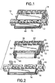
- FIG. 1 there is shown a perspective view of an electrical connector 10 incorporating features of the present invention.
- an electrical connector 10 incorporating features of the present invention.
- the present invention will be described with reference to the embodiments shown in the drawings, it should be understood that the present invention can be embodied in many alternate forms of embodiments.
- any suitable size, shape or type of elements or materials could be used.
- the connector 10 generally comprises two subassemblies 12, 14.
- the first subassembly 12 generally comprises an outer housing piece 16 and an extended shield shell 18.
- the second subassembly 14 generally comprises a housing 20 and electrical contacts 22.
- the housing 20 generally comprises a first member 24 and a second member 26.
- the first member 24 generally comprises a one-piece molded plastic member.
- the first member could be comprised of any suitable material or combination of materials and, could be comprised of multiple pieces.
- the first member 24 has a general right turn shape wherein a first end 28 is offset about 90° from a second end 30.
- the first member 24 could have any suitable shape including being straight, such as for a vertical electrical connector rather than a right angle connector.
- the first member 24 comprises three sections 32, 33, 34 angled relative to each other in series, such as at 45° angles.
- the first member 24 forms an inner side 36 and an outer side 38.
- First member 24 acts as a comb for locating the contacts 22.
- the first member 24 includes contact receiving channels 40, 42, extending into the first member along the two sides 36, 38 and along all three sections 32, 33, 34.
- the channels 40, 42 preferably have a general V shape and alternatingly vary in depth along each side 36, 38 at the section 32.
- adjacent channels 40a and 40b, at section 32 have different depths into the first member.
- Adjacent channels 42a and 42b at section 32 also have different depths.
- the channels 40a, 40b and 42a, 42b have the same depth at the opposite section 34.
- the transition in depth occurs at a junction with or along the middle section 33.
- any suitable depths and/or transitions in depth of the channels could be provided.
- only one side 36 or 38 need be provided with contact receiving channels.
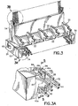
- the contacts 22 are placed within grooves 40, 42 as described in more detail below.
- the contacts 22 are generally stamped and formed from a sheet of suitabel conductive material, such as a copper alloy, but my suitable process and/or materials could be used to form the contacts.
- the contacts 22 each comprise a first connection or mounting section 44, an opposite second connection or mounting section 46, and a middle section 48 therebetween.
- the first connection sections 44 are provided as through-hole solder tails intended to be inserted into holes in a printed circuit board (not shown) and soldered thereto.
- the first connection section 44 could have any suitable shape, such as a spring contact or a surface mount solder tail.
- the middle sections 48 are located in the channels 40, 42.
- the contacts 22 have retainment barbs (not shown) to at least temporarily attach the contacts 22 to the first member 24 in the channels 40, 42.
- the second connection sections 46 are provided as two rows of spring contact beam sections forming a receiving area 50 therebetween for removably receiving a portion of a mating electrical connector (not shown).
- the second member 26 of the housing 20 is molded onto or over the first member 24 with contacts 22 inserted therein.
- the second housing member 26 generally comprises a first section 52, and a second section 54.
- the first section 52 generally comprises supports 56, 58, side latches 60, and recesses 62.
- the supports 56, 58 are provided to help stabilize mounting of the housing 20 on a surface of a printed circuit board or other electronic component.
- the recesses 62 are merely provided to save material and make the connector light weight.
- the first section 52 surrounds the first member 24 at the first and middle sections 32, 33 except at the end 28.
- top side 38 at the middle section 33 is also not covered by the material of the second member 26; merely because of the first member 24 being contacted at that location by a mold used during forming of the second member 26.
- the second section 54 generally surrounds the front section 34 of the first member 24 except at the end 30.
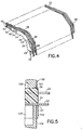
- the second member 26 is molded onto the first member 24. More specifically, after the contacts 22 are inserted into the channels 40, 42, the assembly is inserted into a mold and the second member 26 is formed by injecting plastic into the mold and onto the first member 24. As seen in Fig. 5, the molding apparatus 100 includes dies 102, 104 that clamp onto portions of the first member 24. This forms open areas, such as areas 106, 107, in which plastic material can be injection molded to form the second member 26. The dies 102, 104 contact the first member 24 at specific locations and also contact the contacts 22 at specific locations. Referring particularly to Figs.
- the dies 102, 104 contact the surfaces 64, 65, 66 in the outside of the end 28 and surfaces 67 inside channels 40, 42 at the end 28.
- the first member 24 is used to form a seal with the dies 102, 104 at these locations to prevent the material which is being used to form the second member 26 from being injected near the location L where the contacts exit the channels 40, 42 at the end 28.
- the die 102 can have two types of projections 102a, 102b which are sized and shaped to fit inside respective ones of the channels 40a, 40b when the die 102 is moved into contact with the first member 24 as illustrated by arrow X.
- the die 104 can have projections similar to projections 102a, 102b which are sized and shaped to fit inside respective ones of the channels 42a, 42b, proximate, but slight spaced from the end 28.
- the first member 24 is used to form a seal with the dies at the front end 30 to prevent the material which is being used to form the second member 26 from being injected near the location M where the contacts 22 exit the channels 40, 42 at the end 30.
- the die 102 can have an appropirate shaped section 102c for contacting the tops of the contacts 22 and the first member 24 proximate the end 30.
- the die 104 can have a similar section.
- the ends 28, 30 of the first member 24 extend out of the second member 26.
- use of the first member 24 as a seal with the molding apparatus prevents the ends 44, 46 of the contacts from being substantially disturbed during the process of molding the second member 26 onto the first member 24. Without this sealing function, the contact ends 44, 46 could be disturbed thereby preventing proper connection to other components. For example, the ends 44 could be misaligned such that they are not easily inserted into an array of holes in a printed circuit board.
- the ends 46 on opposite sides of the rows could be positioned too close to each other, thereby blocking an insertion path into area 50 and possibly causing stubbing, or could be positioned too far away from each other, thereby preventing proper wiping, normal force or connection with a mating connector.
- relatively small spacings or pitch such as 0.4 mm or less
- precision or tolerances must be very precise.
- the second subassembly 14 has rails 70 along the lateral sides of the second section 54.
- the first subassembly 12 has slots 72 to receive the rails 70.
- the front ends 46 of the contacts and the front end 30 of the first member 24 are inserted into a main receiving slot 74 of the outer housing piece 16 with the two subassemblies 12, 14 latching to each other to form the connector 10.
- any suitable means could be used to connect the two subassemblies 12, 14 to each other.
- the connector 10 can be used with a second connector 76 to form a dual or double deck connector 78.
- the second connector 76 in this embodiment, is also a right angle connector and generally comprises a housing 80, electrical contacts 82, and a shield shell 84.
- the surfaces 59 can abut against the rear end of the housing 80 to help position the two connectors 10, 76 relative to each other.
- Center sections 83 of the contacts 82 can also extend in areas 57 (see Fig.3).
- the shield shell 84 is connected to the housing 80 and includes side connector sections 86, 87 for connection to the latches 60 of the first connector 10.
- This new connector 78 forms a double deck electrical connector.
Landscapes
- Engineering & Computer Science (AREA)
- Manufacturing & Machinery (AREA)
- Manufacturing Of Electrical Connectors (AREA)
- Connector Housings Or Holding Contact Members (AREA)
Applications Claiming Priority (2)
| Application Number | Priority Date | Filing Date | Title |
|---|---|---|---|
| US451448 | 1995-05-26 | ||
| US09/451,448 US6200171B1 (en) | 1999-11-30 | 1999-11-30 | Electrical connector with over-molded housing member and method of over-molding |
Publications (3)
| Publication Number | Publication Date |
|---|---|
| EP1113534A2 EP1113534A2 (en) | 2001-07-04 |
| EP1113534A3 EP1113534A3 (en) | 2002-02-27 |
| EP1113534B1 true EP1113534B1 (en) | 2007-02-28 |
Family
ID=23792259
Family Applications (1)
| Application Number | Title | Priority Date | Filing Date |
|---|---|---|---|
| EP00124341A Expired - Lifetime EP1113534B1 (en) | 1999-11-30 | 2000-11-17 | Electrical connector with over-molded housing member and method of over-molding |
Country Status (7)
Families Citing this family (22)
| Publication number | Priority date | Publication date | Assignee | Title |
|---|---|---|---|---|
| US6386926B1 (en) * | 2001-06-19 | 2002-05-14 | Su-Lan Yang Lee | Serial bus connector terminal main body |
| US6402552B1 (en) | 2001-08-07 | 2002-06-11 | Fci Americas Technology, Inc. | Electrical connector with overmolded and snap locked pieces |
| US6625881B2 (en) * | 2001-09-11 | 2003-09-30 | Xytrans, Inc. | Solderless method for transferring high frequency, radio frequency signals between printed circuit boards |
| US6788171B2 (en) * | 2002-03-05 | 2004-09-07 | Xytrans, Inc. | Millimeter wave (MMW) radio frequency transceiver module and method of forming same |
| GB2395372B (en) * | 2002-11-13 | 2005-08-31 | Contour Electronics Ltd | Connector |
| DE10260241B4 (de) * | 2002-12-20 | 2013-05-08 | Continental Automotive Gmbh | Kontaktierungsbauteil und Verfahren zur Herstellung eines Kontaktierungsbauteils |
| TW579098U (en) * | 2003-06-18 | 2004-03-01 | Hon Hai Prec Ind Co Ltd | Cable connector assembly |
| US6746255B1 (en) * | 2003-08-01 | 2004-06-08 | Hon Hai Precision Ind. Co., Ltd. | Serial ATA cable assembly |
| US6899564B2 (en) * | 2003-09-30 | 2005-05-31 | Hon Hai Precision Ind. Co., Ltd. | Reinforced serial ATA connector |
| US20050255759A1 (en) * | 2004-05-17 | 2005-11-17 | Lai Ming C | Electrical connector terminal |
| EP1949508B1 (en) * | 2005-10-26 | 2014-08-27 | Federal-Mogul Corporation | Molded lamp socket |
| US7744380B2 (en) | 2007-02-21 | 2010-06-29 | Fci Americas Technology, Inc | Overmolded electrical contact array |
| US7575445B2 (en) * | 2007-02-21 | 2009-08-18 | Fci Americas Technology, Inc. | Contact protector |
| CN101350470A (zh) * | 2007-07-19 | 2009-01-21 | 富士康(昆山)电脑接插件有限公司 | 电连接器及其制造方法 |
| TWM357751U (en) * | 2008-12-26 | 2009-05-21 | Dragonstate Technology Co Ltd | Electrical connector with terminal positioning |
| US8435050B2 (en) * | 2011-04-25 | 2013-05-07 | Apple Inc. | USB connector having vertical to horizontal conversion contacts |
| US9325097B2 (en) * | 2012-11-16 | 2016-04-26 | Apple Inc. | Connector contacts with thermally conductive polymer |
| US8898897B2 (en) | 2013-02-12 | 2014-12-02 | Joseph Lai | Method of making user-friendly USB male connector |
| JP6142412B2 (ja) * | 2013-06-06 | 2017-06-07 | ホシデン株式会社 | コネクタ |
| US9362638B2 (en) | 2014-09-03 | 2016-06-07 | Amphenol Corporation | Overmolded contact wafer and connector |
| US20160190722A1 (en) * | 2014-12-24 | 2016-06-30 | Yazaki Corporation | Connector |
| JP7386917B2 (ja) * | 2022-03-31 | 2023-11-27 | 三菱電機株式会社 | コネクタ |
Family Cites Families (17)
| Publication number | Priority date | Publication date | Assignee | Title |
|---|---|---|---|---|
| US3945708A (en) | 1975-03-28 | 1976-03-23 | International Telephone And Telegraph Corporation | Electrical connector with premold |
| US4579404A (en) * | 1983-09-26 | 1986-04-01 | Amp Incorporated | Conductor-terminated card edge connector |
| US4602831A (en) * | 1983-09-26 | 1986-07-29 | Amp Incorporated | Electrical connector and method of making same |
| US4737117A (en) * | 1983-09-26 | 1988-04-12 | Amp Incorporated | Double-row electrical connector and method of making same |
| US4684202A (en) | 1986-08-25 | 1987-08-04 | General Motors Corporation | Overmolded electrical connector |
| US4865562A (en) | 1988-02-01 | 1989-09-12 | Minnesota Mining And Manufacturing Company | Overmolded electrical contact for the manufacture of connectors |
| JP3404832B2 (ja) * | 1993-10-15 | 2003-05-12 | 住友電装株式会社 | コネクタの製造方法及びコネクタ |
| US5619012A (en) | 1993-12-10 | 1997-04-08 | Philips Electronics North America Corporation | Hinged circuit assembly with multi-conductor framework |
| GB9408755D0 (en) | 1994-05-03 | 1994-06-22 | Amp Gmbh | Integral seal and strain relief member for a connector |
| JP2932152B2 (ja) | 1994-07-19 | 1999-08-09 | モレックス インコーポレーテッド | 電気コネクタに於ける端子及び電気コネクタの形成方法 |
| US5647751A (en) | 1995-06-30 | 1997-07-15 | Shulman; Michael Y. | Female receptacle and premold therefor |
| US5722861A (en) * | 1996-02-28 | 1998-03-03 | Molex Incorporated | Electrical connector with terminals of varying lengths |
| US5902136A (en) | 1996-06-28 | 1999-05-11 | Berg Technology, Inc. | Electrical connector for use in miniaturized, high density, and high pin count applications and method of manufacture |
| US5882214A (en) * | 1996-06-28 | 1999-03-16 | The Whitaker Corporation | Electrical connector with contact assembly |
| US5795191A (en) | 1996-09-11 | 1998-08-18 | Preputnick; George | Connector assembly with shielded modules and method of making same |
| JP3509444B2 (ja) * | 1997-01-13 | 2004-03-22 | 住友電装株式会社 | インサート成形コネクタ |
| US6033258A (en) * | 1998-04-01 | 2000-03-07 | Hon Hai Precision Ind. Co., Ltd. | Stacked connector assembly |
-
1999
- 1999-11-30 US US09/451,448 patent/US6200171B1/en not_active Expired - Fee Related
-
2000
- 2000-11-17 DE DE60033621T patent/DE60033621T2/de not_active Expired - Lifetime
- 2000-11-17 AT AT00124341T patent/ATE355634T1/de not_active IP Right Cessation
- 2000-11-17 EP EP00124341A patent/EP1113534B1/en not_active Expired - Lifetime
- 2000-11-24 CA CA002326850A patent/CA2326850C/en not_active Expired - Fee Related
- 2000-11-28 JP JP2000361465A patent/JP2001185270A/ja active Pending
- 2000-11-29 KR KR1020000071473A patent/KR20010052003A/ko not_active Ceased
Also Published As
| Publication number | Publication date |
|---|---|
| JP2001185270A (ja) | 2001-07-06 |
| CA2326850A1 (en) | 2001-05-30 |
| CA2326850C (en) | 2008-05-13 |
| ATE355634T1 (de) | 2006-03-15 |
| US6200171B1 (en) | 2001-03-13 |
| EP1113534A2 (en) | 2001-07-04 |
| DE60033621T2 (de) | 2007-11-29 |
| DE60033621D1 (de) | 2007-04-12 |
| KR20010052003A (en) | 2001-06-25 |
| EP1113534A3 (en) | 2002-02-27 |
Similar Documents
| Publication | Publication Date | Title |
|---|---|---|
| EP1113534B1 (en) | Electrical connector with over-molded housing member and method of over-molding | |
| US5580283A (en) | Electrical connector having terminal modules | |
| US5975917A (en) | Method for manufacturing an electrical connector and electrical connector manufactured by the same | |
| US5664968A (en) | Connector assembly with shielded modules | |
| US6764336B2 (en) | Method for forming an electrical connector and an electrical connector obtained thereby | |
| EP0854549B1 (en) | Surface mount connector with integrated PCB assembly | |
| US4580868A (en) | Keying system for electrical connectors | |
| KR970001616B1 (ko) | 전기 접속자 어셈블리 | |
| US5779505A (en) | Electrical connector terminal and method of making electrical connector with same | |
| US6402552B1 (en) | Electrical connector with overmolded and snap locked pieces | |
| US6210218B1 (en) | Electrical connector | |
| US6241556B1 (en) | Retention member for connector | |
| US6155886A (en) | Electrical connector and method for making the same | |
| KR101168093B1 (ko) | 커넥터 및 케이블 리테이너 | |
| EP2160802B1 (en) | Electrical connector module | |
| CN111628312B (zh) | 链式端子及具备链式端子中的端子的基板用连接器 | |
| US6588100B2 (en) | Method for forming an electrical connector and an electrical connector obtained thereby | |
| US7112072B2 (en) | Ground bus for an electrical connector | |
| US7188408B2 (en) | Method of making a straddle mount connector | |
| US7458148B2 (en) | Joint connector and method assembling the same | |
| US20050026474A1 (en) | Electrical connector having improved terminals | |
| EP1107373B1 (en) | Press-fit connector | |
| US6033236A (en) | Shielded connector | |
| US5190483A (en) | Contact retention | |
| CN114142286A (zh) | 一种线缆连接器及连接器组件 |
Legal Events
| Date | Code | Title | Description |
|---|---|---|---|
| PUAI | Public reference made under article 153(3) epc to a published international application that has entered the european phase |
Free format text: ORIGINAL CODE: 0009012 |
|
| AK | Designated contracting states |
Kind code of ref document: A2 Designated state(s): AT BE CH CY DE DK ES FI FR GB GR IE IT LI LU MC NL PT SE TR |
|
| AX | Request for extension of the european patent |
Free format text: AL;LT;LV;MK;RO;SI |
|
| PUAL | Search report despatched |
Free format text: ORIGINAL CODE: 0009013 |
|
| AK | Designated contracting states |
Kind code of ref document: A3 Designated state(s): AT BE CH CY DE DK ES FI FR GB GR IE IT LI LU MC NL PT SE TR |
|
| AX | Request for extension of the european patent |
Free format text: AL;LT;LV;MK;RO;SI |
|
| RIC1 | Information provided on ipc code assigned before grant |
Free format text: 7H 01R 13/405 A, 7H 01R 13/504 B, 7H 01R 43/24 B |
|
| 17P | Request for examination filed |
Effective date: 20020819 |
|
| AKX | Designation fees paid |
Free format text: AT BE CH CY DE DK ES FI FR GB GR IE IT LI LU MC NL PT SE TR |
|
| GRAP | Despatch of communication of intention to grant a patent |
Free format text: ORIGINAL CODE: EPIDOSNIGR1 |
|
| GRAS | Grant fee paid |
Free format text: ORIGINAL CODE: EPIDOSNIGR3 |
|
| GRAA | (expected) grant |
Free format text: ORIGINAL CODE: 0009210 |
|
| RAP1 | Party data changed (applicant data changed or rights of an application transferred) |
Owner name: FCI |
|
| AK | Designated contracting states |
Kind code of ref document: B1 Designated state(s): AT BE CH CY DE DK ES FI FR GB GR IE IT LI LU MC NL PT SE TR |
|
| PG25 | Lapsed in a contracting state [announced via postgrant information from national office to epo] |
Ref country code: CH Free format text: LAPSE BECAUSE OF FAILURE TO SUBMIT A TRANSLATION OF THE DESCRIPTION OR TO PAY THE FEE WITHIN THE PRESCRIBED TIME-LIMIT Effective date: 20070228 Ref country code: LI Free format text: LAPSE BECAUSE OF FAILURE TO SUBMIT A TRANSLATION OF THE DESCRIPTION OR TO PAY THE FEE WITHIN THE PRESCRIBED TIME-LIMIT Effective date: 20070228 Ref country code: FI Free format text: LAPSE BECAUSE OF FAILURE TO SUBMIT A TRANSLATION OF THE DESCRIPTION OR TO PAY THE FEE WITHIN THE PRESCRIBED TIME-LIMIT Effective date: 20070228 Ref country code: DK Free format text: LAPSE BECAUSE OF FAILURE TO SUBMIT A TRANSLATION OF THE DESCRIPTION OR TO PAY THE FEE WITHIN THE PRESCRIBED TIME-LIMIT Effective date: 20070228 Ref country code: AT Free format text: LAPSE BECAUSE OF FAILURE TO SUBMIT A TRANSLATION OF THE DESCRIPTION OR TO PAY THE FEE WITHIN THE PRESCRIBED TIME-LIMIT Effective date: 20070228 Ref country code: BE Free format text: LAPSE BECAUSE OF FAILURE TO SUBMIT A TRANSLATION OF THE DESCRIPTION OR TO PAY THE FEE WITHIN THE PRESCRIBED TIME-LIMIT Effective date: 20070228 Ref country code: NL Free format text: LAPSE BECAUSE OF FAILURE TO SUBMIT A TRANSLATION OF THE DESCRIPTION OR TO PAY THE FEE WITHIN THE PRESCRIBED TIME-LIMIT Effective date: 20070228 |
|
| REG | Reference to a national code |
Ref country code: GB Ref legal event code: FG4D |
|
| REG | Reference to a national code |
Ref country code: CH Ref legal event code: EP |
|
| REF | Corresponds to: |
Ref document number: 60033621 Country of ref document: DE Date of ref document: 20070412 Kind code of ref document: P |
|
| REG | Reference to a national code |
Ref country code: IE Ref legal event code: FG4D |
|
| PG25 | Lapsed in a contracting state [announced via postgrant information from national office to epo] |
Ref country code: SE Free format text: LAPSE BECAUSE OF FAILURE TO SUBMIT A TRANSLATION OF THE DESCRIPTION OR TO PAY THE FEE WITHIN THE PRESCRIBED TIME-LIMIT Effective date: 20070531 |
|
| PG25 | Lapsed in a contracting state [announced via postgrant information from national office to epo] |
Ref country code: ES Free format text: LAPSE BECAUSE OF FAILURE TO SUBMIT A TRANSLATION OF THE DESCRIPTION OR TO PAY THE FEE WITHIN THE PRESCRIBED TIME-LIMIT Effective date: 20070608 |
|
| ET | Fr: translation filed | ||
| PG25 | Lapsed in a contracting state [announced via postgrant information from national office to epo] |
Ref country code: PT Free format text: LAPSE BECAUSE OF FAILURE TO SUBMIT A TRANSLATION OF THE DESCRIPTION OR TO PAY THE FEE WITHIN THE PRESCRIBED TIME-LIMIT Effective date: 20070730 |
|
| NLV1 | Nl: lapsed or annulled due to failure to fulfill the requirements of art. 29p and 29m of the patents act | ||
| REG | Reference to a national code |
Ref country code: CH Ref legal event code: PL |
|
| PLBE | No opposition filed within time limit |
Free format text: ORIGINAL CODE: 0009261 |
|
| STAA | Information on the status of an ep patent application or granted ep patent |
Free format text: STATUS: NO OPPOSITION FILED WITHIN TIME LIMIT |
|
| 26N | No opposition filed |
Effective date: 20071129 |
|
| PG25 | Lapsed in a contracting state [announced via postgrant information from national office to epo] |
Ref country code: GR Free format text: LAPSE BECAUSE OF FAILURE TO SUBMIT A TRANSLATION OF THE DESCRIPTION OR TO PAY THE FEE WITHIN THE PRESCRIBED TIME-LIMIT Effective date: 20070529 Ref country code: IT Free format text: LAPSE BECAUSE OF FAILURE TO SUBMIT A TRANSLATION OF THE DESCRIPTION OR TO PAY THE FEE WITHIN THE PRESCRIBED TIME-LIMIT Effective date: 20070228 |
|
| PG25 | Lapsed in a contracting state [announced via postgrant information from national office to epo] |
Ref country code: MC Free format text: LAPSE BECAUSE OF NON-PAYMENT OF DUE FEES Effective date: 20071130 |
|
| PG25 | Lapsed in a contracting state [announced via postgrant information from national office to epo] |
Ref country code: IE Free format text: LAPSE BECAUSE OF NON-PAYMENT OF DUE FEES Effective date: 20071119 |
|
| PG25 | Lapsed in a contracting state [announced via postgrant information from national office to epo] |
Ref country code: CY Free format text: LAPSE BECAUSE OF FAILURE TO SUBMIT A TRANSLATION OF THE DESCRIPTION OR TO PAY THE FEE WITHIN THE PRESCRIBED TIME-LIMIT Effective date: 20070228 |
|
| PG25 | Lapsed in a contracting state [announced via postgrant information from national office to epo] |
Ref country code: LU Free format text: LAPSE BECAUSE OF NON-PAYMENT OF DUE FEES Effective date: 20071117 |
|
| PG25 | Lapsed in a contracting state [announced via postgrant information from national office to epo] |
Ref country code: TR Free format text: LAPSE BECAUSE OF FAILURE TO SUBMIT A TRANSLATION OF THE DESCRIPTION OR TO PAY THE FEE WITHIN THE PRESCRIBED TIME-LIMIT Effective date: 20070228 |
|
| REG | Reference to a national code |
Ref country code: FR Ref legal event code: CA |
|
| PGFP | Annual fee paid to national office [announced via postgrant information from national office to epo] |
Ref country code: FR Payment date: 20121113 Year of fee payment: 13 |
|
| REG | Reference to a national code |
Ref country code: FR Ref legal event code: ST Effective date: 20140731 |
|
| PG25 | Lapsed in a contracting state [announced via postgrant information from national office to epo] |
Ref country code: FR Free format text: LAPSE BECAUSE OF NON-PAYMENT OF DUE FEES Effective date: 20131202 |
|
| PGFP | Annual fee paid to national office [announced via postgrant information from national office to epo] |
Ref country code: DE Payment date: 20151130 Year of fee payment: 16 Ref country code: GB Payment date: 20151027 Year of fee payment: 16 |
|
| REG | Reference to a national code |
Ref country code: DE Ref legal event code: R119 Ref document number: 60033621 Country of ref document: DE |
|
| GBPC | Gb: european patent ceased through non-payment of renewal fee |
Effective date: 20161117 |
|
| PG25 | Lapsed in a contracting state [announced via postgrant information from national office to epo] |
Ref country code: GB Free format text: LAPSE BECAUSE OF NON-PAYMENT OF DUE FEES Effective date: 20161117 Ref country code: DE Free format text: LAPSE BECAUSE OF NON-PAYMENT OF DUE FEES Effective date: 20170601 |