EP1113494A1 - Dispositif de protection de lignes d'interconnexions dans un circuit intégré - Google Patents
Dispositif de protection de lignes d'interconnexions dans un circuit intégré Download PDFInfo
- Publication number
- EP1113494A1 EP1113494A1 EP00403692A EP00403692A EP1113494A1 EP 1113494 A1 EP1113494 A1 EP 1113494A1 EP 00403692 A EP00403692 A EP 00403692A EP 00403692 A EP00403692 A EP 00403692A EP 1113494 A1 EP1113494 A1 EP 1113494A1
- Authority
- EP
- European Patent Office
- Prior art keywords
- lines
- line
- interconnection
- memory
- witness
- Prior art date
- Legal status (The legal status is an assumption and is not a legal conclusion. Google has not performed a legal analysis and makes no representation as to the accuracy of the status listed.)
- Withdrawn
Links
- 239000000758 substrate Substances 0.000 claims abstract description 23
- 238000004519 manufacturing process Methods 0.000 claims abstract description 20
- 230000015654 memory Effects 0.000 claims description 79
- 229910052751 metal Inorganic materials 0.000 claims description 23
- 239000002184 metal Substances 0.000 claims description 23
- 229910021420 polycrystalline silicon Inorganic materials 0.000 claims description 21
- 229920005591 polysilicon Polymers 0.000 claims description 21
- 230000005764 inhibitory process Effects 0.000 claims description 17
- 230000001681 protective effect Effects 0.000 claims description 12
- 102100026396 ADP/ATP translocase 2 Human genes 0.000 claims description 11
- 101000718417 Homo sapiens ADP/ATP translocase 2 Proteins 0.000 claims description 11
- 239000000463 material Substances 0.000 claims description 5
- 101100328884 Caenorhabditis elegans sqt-3 gene Proteins 0.000 claims description 2
- 102100032533 ADP/ATP translocase 1 Human genes 0.000 description 10
- 101000768061 Escherichia phage P1 Antirepressor protein 1 Proteins 0.000 description 10
- 101000796932 Homo sapiens ADP/ATP translocase 1 Proteins 0.000 description 10
- 208000019300 CLIPPERS Diseases 0.000 description 8
- 208000021930 chronic lymphocytic inflammation with pontine perivascular enhancement responsive to steroids Diseases 0.000 description 8
- 238000000034 method Methods 0.000 description 7
- 102100026397 ADP/ATP translocase 3 Human genes 0.000 description 6
- 101000718437 Homo sapiens ADP/ATP translocase 3 Proteins 0.000 description 6
- 238000009792 diffusion process Methods 0.000 description 5
- 238000005516 engineering process Methods 0.000 description 4
- 238000005530 etching Methods 0.000 description 4
- 239000011159 matrix material Substances 0.000 description 4
- 238000004140 cleaning Methods 0.000 description 3
- 230000000694 effects Effects 0.000 description 3
- 230000006870 function Effects 0.000 description 3
- 230000009931 harmful effect Effects 0.000 description 3
- 230000015556 catabolic process Effects 0.000 description 2
- 230000006378 damage Effects 0.000 description 2
- 238000010586 diagram Methods 0.000 description 2
- 239000012530 fluid Substances 0.000 description 2
- 230000035945 sensitivity Effects 0.000 description 2
- 101100328886 Caenorhabditis elegans col-2 gene Proteins 0.000 description 1
- 229910052782 aluminium Inorganic materials 0.000 description 1
- XAGFODPZIPBFFR-UHFFFAOYSA-N aluminium Chemical compound [Al] XAGFODPZIPBFFR-UHFFFAOYSA-N 0.000 description 1
- 238000000137 annealing Methods 0.000 description 1
- 230000015572 biosynthetic process Effects 0.000 description 1
- 235000014510 cooky Nutrition 0.000 description 1
- 238000001816 cooling Methods 0.000 description 1
- 238000001514 detection method Methods 0.000 description 1
- 230000009977 dual effect Effects 0.000 description 1
- 230000006872 improvement Effects 0.000 description 1
- 239000003112 inhibitor Substances 0.000 description 1
- 238000010849 ion bombardment Methods 0.000 description 1
- 239000007788 liquid Substances 0.000 description 1
- 238000001465 metallisation Methods 0.000 description 1
- 230000008520 organization Effects 0.000 description 1
- 244000045947 parasite Species 0.000 description 1
- 238000001020 plasma etching Methods 0.000 description 1
- 230000008569 process Effects 0.000 description 1
- 230000009467 reduction Effects 0.000 description 1
Images



Classifications
-
- H—ELECTRICITY
- H10—SEMICONDUCTOR DEVICES; ELECTRIC SOLID-STATE DEVICES NOT OTHERWISE PROVIDED FOR
- H10D—INORGANIC ELECTRIC SEMICONDUCTOR DEVICES
- H10D89/00—Aspects of integrated devices not covered by groups H10D84/00 - H10D88/00
- H10D89/60—Integrated devices comprising arrangements for electrical or thermal protection, e.g. protection circuits against electrostatic discharge [ESD]
- H10D89/601—Integrated devices comprising arrangements for electrical or thermal protection, e.g. protection circuits against electrostatic discharge [ESD] for devices having insulated gate electrodes, e.g. for IGFETs or IGBTs
- H10D89/811—Integrated devices comprising arrangements for electrical or thermal protection, e.g. protection circuits against electrostatic discharge [ESD] for devices having insulated gate electrodes, e.g. for IGFETs or IGBTs using FETs as protective elements
Definitions
- the present invention relates to a device for protection of interconnection lines in a circuit integrated, to protect elements connected to these lines against electrostatic charges generated on these lines during circuit manufacturing integrated.
- each cell is controlled by a line of bit and a word line from memory.
- the lines of word and bit lines are driven by outputs a decoder.
- Each cell can thus be read or written individually, by selecting the line of bit and the corresponding word line by a memory address decoding circuit.
- a byte is made up of eight cells located on the same word line Wl, at the intersection of eight consecutive bit lines.
- Typical EEPROM memory architectures also include source lines, of metal, which contact cell source broadcasts memory, to draw these sources to earth, in reading especially. These source lines run through the plane memory longitudinally. They are usually made of metal. They are connected at the periphery from the memory plane to a grounding transistor controlled by a mode function control signal access to memory.
- the matrix organization combines a grouping bit lines into columns. This allows simultaneous access to several cells, typically eight, forming a memory word (byte).
- Such a architecture requires additional transistors each allowing the selection of a column particular memory.
- a control line by column i.e. by group of eight bit lines, with a selection transistor column by word line.
- These control lines also go through the memory map longitudinally. They are usually performed made of metal.
- an EEPROM memory plan includes usually as interconnection lines running the whole memory plane (in one dimension of it), bit lines, word lines, lines of control, and the source lines.
- the cells of two consecutive columns are represented, located on the same word line Wl k.
- an EEPROM memory cell usually includes (at least) a transistor access Ta in series with a gate transistor floating Tf.
- the access transistor is connected on its grid to the corresponding word line, and on its drain, at the corresponding bit line.
- the first column Col1 comprises eight cells C0 to C7 placed on the word line Wl k.
- the first cell C0 is connected to the bit line Bl0
- the second cell C1 is connected to the bit line Bl1, and so on until the last cell C7 which is connected to the bit line Bl7.
- All the floating gate transistors of these cells C0 to C7 have a common source diffusion, connected to the source line associated with the column, LS i .
- a column selection transistor TC k, i is connected between the control line CG i associated with the column and the common gate of the floating gate transistors of cells C0 to C7.
- the second column Col2 is of identical structure. In the example, it is performed in the memory plane symmetrically. Thus, from left to right, there is the source line LS i of the first column, the eight bit lines Bl0 to Bl7, the control line CG i of the first column, the control line CG i + 1 of the second column, eight bit lines Bl0 to Bl7, and the source line LS i + 1 in this column.
- a first harmful effect is the damage or destruction of active elements of these cells: junctions, gate oxide, tunnel oxide, which causes leakage of these elements (junctions, gate oxide) or even breakdown (tunnel oxide). These harmful effects are more generally found in any integrated circuit comprising interconnection lines connected to electronic elements.
- Another harmful effect is the reduction of the cycle of memory cell life.
- the significant increase in potential on these lines due to loads electrostatic can have the same effect as a large number of read and / or write access, reducing correspondingly the guaranteed lifetime for these cells.
- the wafer In the plasma etching step, the wafer is subjected to ion bombardment, which can lead to an increase in surface potential. Of special precautions are usually taken to prevent this potential increase, including the application of a magnetic field in the engraving enclosure. But these precautions prove in practice insufficient.
- the friction of the cleaning fluid can cause electrostatic charges, by triboelectricity.
- the known use of a conductive fluid does not allow not solve this problem satisfactorily.
- an object of the invention is to solve the problem of the appearance of electrostatic charges on interconnect lines of an integrated circuit.
- the idea underlying the invention is a device active protection during the manufacturing of the integrated circuit to protect a line interconnection.
- the invention therefore relates to a device for protection of a circuit interconnection line integrated characterized in that it comprises a device load flow connected to the line interconnection to protect and a line witness interconnection to trigger said flow device, protective device being active throughout the manufacturing of the circuit integrated.
- the same line interconnection indicator is connected to a number limited flow devices, so as not to alter the sensitivity of the witness interconnection line.
- Figure 3 shows a device 1 of protection according to the invention of a line Li interconnection.
- This protection device 1 comprises mainly a device 2 for flow of charges to the integrated circuit substrate and a line ANT indicator interconnection to trigger the charge flow device.
- the flow device of charges includes an N type MOS M1 transistor connected between the interconnection line to be protected and the substrate, which is schematically represented by a down arrow.
- This MOS transistor M1 is controlled on its grid by the ANT witness interconnection line.
- the protective device is required to ensure its function during manufacture of the integrated circuit, while the integrated circuit is not supplied.
- the substrate at this time is therefore not polarized.
- the protective device according to the invention is thus a active device, which draws its energy from the charges electrostatic themselves.
- the device for protection further includes an E1 clipper, for limit the voltage on the interconnection line witness. Indeed, it is necessary that the tension on the grid of transistor M1 remains below the voltage of breakdown of the gate oxide.
- This clipper will be by example sized to trip around 15 volts.
- This clipper we will use devices similar to those used to protect the input pads of integrated circuits, against electrostatic discharge, but moreover small dimensions, the quantity of charges electrostatic being less in the area of the invention.
- This clipper will, for example, be made of conventionally, by a lateral bipolar transistor, or by means of a simple diode.
- the protective device further comprises a INH inhibitor, to deactivate the protection device when the power is turned on integrated circuit.
- a INH inhibitor to deactivate the protection device when the power is turned on integrated circuit.
- some interconnection lines may be brought to high potentials, like for example, potential for programming memory cells. he the protective device associated with these interconnect lines will fire in operational.
- an inhibition device is provided at least for the lines of interconnection brought to receive strong potentials in operational mode of the circuit integrated.
- This inhibition device is made simple by an N-type Mos M2 transistor whose gate is connected to the logic supply voltage of the integrated circuit, to draw the interconnection line indicator at the substrate bias voltage from the energizing the integrated circuit. In this way, the charge flow device can no longer be activated in operational mode of the integrated circuit. If the MOS transistor M2 is chosen to type P, its grid will be connected to electrical ground of the integrated circuit.
- the transistor M2 of the inhibition device can besides performing the function of the El clipper, in particular due to the structure of lateral bipolar transistor parasite inherent in the structure of the MOS transistor. Also, in the event that the protective device associated with an interconnection line includes such inhibition device, we will not need to additionally provide for the clipper, which enables saving space in the integrated circuit.
- FIG. 4 represents an application of the protection device according to the invention to a group of interconnection lines Li0 to Li6. It includes an ANT antenna, an INH inhibition device and / or a E1 clipper (shown in dotted lines) and as many detection devices M1 0 , ..., M1 6 as there are interconnection lines Li0 to Li6 to be protected.
- the protective device according to the invention makes it possible to protect one or more lines interconnection by means of an interconnection line witness. It works as soon as this line and the associated flow devices are produced. he can be deactivated after manufacturing the circuit integrated, by the INH inhibition device provided for effect, by energizing the integrated circuit.
- the witness interconnection line is carried out near the line (s) interconnection to be protected, for efficiency optimum. Indeed, if the control line is too far from the line to be protected, the associated flow device might go off too late.
- the interconnection line witness is parallel to interconnection lines that it protects, which seems to be the mode of most effective achievement as soon as the line witness may be carried out near these lines.
- the control line does not follow the same direction as the lines it protects.
- the implementation of the invention supposes the taking into account the desired protection efficiency and the increase in surface area required for the implementation of these devices.
- FIG. 5a thus represents an example architecture known from EEPROM memory, in which protection devices have been integrated according to the invention.
- the lines interconnection to protect are on the one hand the lines bit, control lines and source lines, which traverse the memory plane in the direction Ox of the memory plane (i.e. longitudinally) and on the other hand, the word lines, which run through the plane memory in the direction Oy (i.e. horizontally).
- FIG. 2 We have already described an example of the structure of a plane EEPROM memory ( Figure 2).
- Figure 5 Two successive columns of such a memory plan.
- the preceding witness lines ANT1 could be used to protect them as shown in FIG. 5a. It is thus possible to provide that an antenna ANT1 also protects 16 word lines. There would thus be, in a memory plane of 512 bit lines by 512 word lines, 32 witness lines ANT1, each protecting 16 bit lines and the associated control and source lines and 16 word lines.
- the flow device is placed at the intersection of the associated word line and control line. In the example shown (FIG.5a) the flow device thus comprises a transistor M1 20 connected between the word line W10 and the substrate and a transistor M1 21 connected between the word line W11 and the substrate.
- lines are provided cookies different from those used for lines bit, control and source.
- this control line ANT2 is produced at the end of the memory plane, parallel to the bit lines, with a flow device per word line, placed at the end of this word line.
- each flow device is placed at the intersection of the associated word line and this control line ANT2.
- FIG. 5b there is thus a first flow transistor M1 wl0 connected between the word line Wl0 and the substrate and the gate of which is connected to the control line ANT2 and a second transistor M1 Wl1 connected between the word line Wl1 and the substrate and the grid of which is connected to the control line ANT2.
- the corresponding M2 ANT2 inhibition device is placed at the end of the control line.
- FIG 6 there is shown another mode of realization of the witness lines associated with the lines of word.
- This witness line is therefore parallel to these lines. So, we has a witness line for two successive word lines of the memory plan. This achievement is very effective but very expensive, since for a memory plan of 512 word lines it requires the completion of 251 witness lines.
- the flow devices and the inhibition device are placed on the periphery of the memory plane.
- a first flow transistor M1 ′ Wl0 is thus represented connected between the word line Wl0 and the substrate and the gate of which is connected to the control line ANT3 and a second transistor M1 ′ Wl1 connected between the line of word Wl1 and the substrate and the grid of which is connected to the control line ANT3.
- the corresponding M2 ANT3 inhibition device is placed at the end of the ANT3 control line.
- the protective device associated with one or more bit lines to be effective as soon as these lines are manufactured the protective device be implemented at the latest in the stage of manufacturing the lines it protects.
- the word lines are in polysilicon, while the bit, source and control lines are in metal.
- the polysilicon layers are made before the metal layers. If we take the example of embodiment shown in FIG. 5a, if the antenna ANT1 is made of metal and is used as a control line for the word lines Wl0 and Wl1 (case shown with the associated flow transistors M1 20 and M1 21 ), the polysilicon lines are not protected between the polysilicon etching step where they are made and the metal etching step where the control line is made.
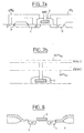
- FIG. 7a an MOS transistor has thus been shown in section which can be used as a transistor in flow devices or in inhibition devices.
- the source diffusion S of the transistor is connected by a metal line LM1 to a substrate socket (diffusion P - in the example).
- the drain diffusion D is connected by a metal line, which may be a bit line Bl0.
- the polysilicon grid is connected to a metal line, which in the example is the control line ANT1.
- Métal1 and Métal2 we plan to carry out preferably the control lines on the same level of metal than the lines it protects.
- the bit lines are made of Metal1 and the source and control lines are made of Metal2, provision is then made to split the witness line ANT1, to make one in metal, to protect the bit lines as soon as they are manufactured and one in Metal2, to protect the control and source lines, the two control lines using the same flow and inhibition devices. It suffices for example to short-circuit these two control lines, as shown in the sectional view of FIG. 7b, on which the two levels of metal of the control line, ANT1 M1 and ANT M2 , and their connections are shown. the gate G of the same flow transistor.
- the lines of word are made in polysilicon.
- the contacts on the transistors are usually made of metal, as shown in Figures 7a and 7b. In this case, make these contacts differently, so that these connections are operational from the stage of manufacturing considered complete, i.e. the step of engraving polysilicon.
- Figure 8 we have shown a well known connection technique, so-called buried contact, which may be used.
- contacting sources and drains is made by polysilicon lines.
- the contact is made by the edge of the drain (or source), with the polysilicon deposited on the surface of the substrate, the annealing of the polysilicon causing the formation of a diode between the polysilicon and the substrate by diffusion of polysilicon doping in the substrate.
- the protection is operational from the engraving stage on polysilicon. It is not useful to use this technique for muting transistors, because these transistors only need to be operational when the integrated circuit is complete and energized. We can therefore use conventional MOS transistors, less expensive in place.
- connection technique by buried contact is especially usable in the exemplary embodiments described, with the control line ANT2 ( Figure 5b) and the ANT3 control line ( Figure 6).
Landscapes
- Non-Volatile Memory (AREA)
- Semiconductor Memories (AREA)
- Semiconductor Integrated Circuits (AREA)
Abstract
Description
jonctions, oxyde de grille, oxyde tunnel, qui entraíne des fuites de ces éléments (jonctions, oxyde de grille) ou même le claquage (oxyde tunnel). Ces effets néfastes se retrouvent plus généralement dans tout circuit intégré comprenant des lignes d'interconnexion connectées à des éléments électroniques.
- La figure 1 déjà décrite représente schématiquement un plan mémoire;
- la figure 2 déjà décrite représente de façon plus détaillée, deux octets successifs dans un plan mémoire de type EEPROM;
- la figure 3 représente un dispositif de protection d'une ligne d'interconnexion selon l'invention;
- la figure 4 représente une variante de réalisation d'un dispositif de protection selon l'invention pour un ensemble de lignes d'interconnexion;
- les figures 5a et 5b représentent des exemples d'application du dispositif de protection selon l'invention à la protection de lignes d'interconnexion dans un plan mémoire;
- la ligne 6 représente un autre mode de réalisation de lignes témoins ;
- les figures 7a et 7b représentent chacune une vue en coupe d'un transistor MOS classique utilisable dans un dispositif de protection selon l'invention; et
- la figure 8 représente la vue en coupe d'un transistor MOS dans lequel les contacts sont réalisés en polysilicium, utilisable dans un dispositif de protection selon l'invention.
Claims (20)
- Dispositif de protection (1) d'une ligne d'interconnexion (Li) d'un circuit intégré, caractérisé en qu'il comprend un dispositif d'écoulement de charges (M1) connecté entre la ligne d'interconnexion à protéger et le substrat du circuit intégré et une ligne d'interconnexion témoin (ANT) pour déclencher ledit dispositif d'écoulement, le dispositif de protection étant actif au long de la fabrication du circuit intégré.
- Dispositif de protection selon la revendication 1, caractérisé en ce que la dite ligne d'interconnexion témoin (ANT) est commune à un ensemble de lignes d'interconnexion à protéger (Li0 à Li6), un dispositif d'écoulement de charges (M10 à M16) étant connecté entre chacune des lignes à protéger et le substrat.
- Dispositif de protection selon la revendication 2, caractérisé en ce que ledit ensemble de lignes d'interconnexion et la ligne témoin associée sont réalisés dans le même matériau.
- Dispositif de protection selon l'une des revendications précédentes, caractérisé en ce que la ou les lignes d'interconnexion et la ligne témoin associée sont réalisées dans la même étape de fabrication.
- Dispositif de protection selon la revendication 3 en combinaison avec la revendication 4,
caractérisé en ce que la ligne d'interconnexion témoin (ANT1) est démultipliée en autant de lignes (ANTM1, ANTM2) que de niveaux de fabrication (Métal1, Métal2) des lignes d'interconnexion. - Dispositif de protection selon l'une quelconque des revendications précédentes, caractérisé en ce qu'il comprend un circuit d'inhibition (INH) connecté entre la ligne d'interconnexion témoin (ANT) et le substrat, et en ce que ce circuit d'inhibition est activé par la mise sous tension du circuit intégré.
- Dispositif de protection selon l'une quelconque des revendications précédentes, caractérisé en ce qu'il comprend en outre un écrêteur de tension (E1) connecté entre la ligne d'interconnexion témoin (ANT) et le substrat.
- Dispositif de protection selon l'une quelconque des revendications précédentes, caractérisé en ce qu'il est utilisé pour protéger des lignes d'interconnexion (Bl0, CG0, LS0, Wl0) d'un plan mémoire.
- Plan mémoire caractérisé en ce qu'il comprend au moins un dispositif de protection selon la revendication 8, pour protéger les lignes d'interconnexion permettant l'accès aux cellules mémoire.
- Plan mémoire selon la revendication 9, organisé matriciellement en lignes de bit et lignes de mot et selon une architecture colonne, comprenant des lignes de bit (Bl0,..., Bl7), une ligne de source (LS1) et une ligne de contrôle (CG0) par colonne (Col0), caractérisé en ce qu'un même dispositif de protection est utilisé pour protéger au moins les lignes de bit, la ligne de source et la ligne de contrôle d'une même colonne, comprenant une ligne témoin (ANT1) et un dispositif d'écoulement par ligne d'interconnexion protégée.
- Plan mémoire selon la revendication 10, caractérisé en ce qu'il comprend un dispositif de protection par deux colonnes successives, la ligne d'interconnexion témoin (ANT1) commune à deux colonnes successives (Col0, Col1) étant géographiquement placée entre ces deux colonnes pour protéger les lignes d'interconnexion correspondantes.
- Plan mémoire selon la revendication 10 ou 11, caractérisé en ce que le dispositif de protection des lignes de bit, des sources et de contrôle est utilisé pour protéger des lignes de mot du plan mémoire, avec un dispositif d'écoulement de charges (M120, M121) pour chaque ligne de mot protégée.
- Plan mémoire selon la revendication 10 ou 11, les lignes de bit, de contrôle et de source étant réalisées en métal, caractérisé en ce que la ligne d'interconnexion témoin (ANT1) est en métal.
- Plan mémoire selon la revendication 13, caractérisé en ce que ladite ligne d'interconnexion témoin (ANT1) est démultipliée en autant de lignes (ANT1M1, ANT1M2) que de niveaux de métal parmi les lignes d'interconnexion protégées.
- Plan mémoire selon l'une quelconque des revendications 9 à 11, caractérisé en ce qu'il comprend un dispositif de protection par deux lignes de mot successives (Wl0, Wl1), comprenant une ligne d'interconnexion témoin (ANT3) placée entre ces deux lignes de mot.
- Plan mémoire selon l'une quelconque des revendications 9 à 11, caractérisé en ce qu'il comprend un dispositif de protection pour l'ensemble des lignes de mot du plan mémoire, comprenant une ligne d'interconnexion témoin (ANT2) placée en bout de plan mémoire.
- Plan mémoire selon la revendication 15 ou 16, les lignes de mot étant en polysilicium, caractérisé en ce que la ligne d'interconnexion témoin correspondante (ANT2, ANT3) est en polysilicium.
- Plan mémoire selon l'une quelconque des revendications 10, 11 ou 13 à 17, caractérisé en ce que les dispositifs d'écoulement de charge des dispositifs de protection sont réalisés en périphérie du plan mémoire.
- Plan mémoire selon l'une quelconque des revendications 10 et 12, chacun des dispositifs de protection ayant sa ligne d'interconnexion témoin (ANT1, ANT2, ANT3) connectée à un dispositif d'inhibition (M2ANT1, M2ANT2, M2ANT3), selon la revendication 6, caractérisé en ce que le ou les dispositifs d'inhibition sont réalisés en périphérie du plan mémoire.
- Circuit intégré comprenant un dispositif de protection ou un plan mémoire selon l'une quelconque des revendications précédentes.
Applications Claiming Priority (2)
| Application Number | Priority Date | Filing Date | Title |
|---|---|---|---|
| FR9916604A FR2803100B1 (fr) | 1999-12-28 | 1999-12-28 | Dispositif de protection de lignes d'interconnexions dans un circuit integre |
| FR9916604 | 1999-12-28 |
Publications (1)
| Publication Number | Publication Date |
|---|---|
| EP1113494A1 true EP1113494A1 (fr) | 2001-07-04 |
Family
ID=9553935
Family Applications (1)
| Application Number | Title | Priority Date | Filing Date |
|---|---|---|---|
| EP00403692A Withdrawn EP1113494A1 (fr) | 1999-12-28 | 2000-12-27 | Dispositif de protection de lignes d'interconnexions dans un circuit intégré |
Country Status (3)
| Country | Link |
|---|---|
| US (1) | US6580594B2 (fr) |
| EP (1) | EP1113494A1 (fr) |
| FR (1) | FR2803100B1 (fr) |
Families Citing this family (1)
| Publication number | Priority date | Publication date | Assignee | Title |
|---|---|---|---|---|
| US7567458B2 (en) * | 2005-09-26 | 2009-07-28 | Silicon Storage Technology, Inc. | Flash memory array having control/decode circuitry for disabling top gates of defective memory cells |
Citations (7)
| Publication number | Priority date | Publication date | Assignee | Title |
|---|---|---|---|---|
| EP0614223A1 (fr) * | 1993-02-17 | 1994-09-07 | STMicroelectronics S.r.l. | Mémoire non-volatile avec diode de protection |
| EP0632560A2 (fr) * | 1993-06-30 | 1995-01-04 | Nec Corporation | Dispositif de circuit intégré à semi-conducteur équipé d'un système de protection pour décharger directement les surtensions des bornes sur une ligne de déchargement |
| US5457336A (en) * | 1994-10-13 | 1995-10-10 | Advanced Micro Devices, Inc. | Non-volatile memory structure including protection and structure for maintaining threshold stability |
| EP0693781A1 (fr) * | 1994-07-13 | 1996-01-24 | United Microelectronics Corporation | Procédé avec mise à la masse pour éliminer l'effet d'antenne pendant la fabrication |
| US5515226A (en) * | 1994-01-25 | 1996-05-07 | Sgs-Thomson Microelectronics, S. A. | Integrated circuit incorporating a system of protection against electrostatic discharges |
| JPH10200077A (ja) * | 1997-01-08 | 1998-07-31 | Sony Corp | 半導体装置及びその製造方法 |
| US5953191A (en) * | 1997-01-31 | 1999-09-14 | Nec Corporation | Protection circuit against electrostatic charge applied between power supply terminals for preventing internal circuit therefrom regardless of polarity thereof |
Family Cites Families (6)
| Publication number | Priority date | Publication date | Assignee | Title |
|---|---|---|---|---|
| US5497146A (en) * | 1992-06-03 | 1996-03-05 | Frontec, Incorporated | Matrix wiring substrates |
| US5668032A (en) * | 1995-07-31 | 1997-09-16 | Holmberg; Scott H. | Active matrix ESD protection and testing scheme |
| US5721656A (en) * | 1996-06-10 | 1998-02-24 | Winbond Electronics Corporation | Electrostatc discharge protection network |
| US5973658A (en) * | 1996-12-10 | 1999-10-26 | Lg Electronics, Inc. | Liquid crystal display panel having a static electricity prevention circuit and a method of operating the same |
| US5991134A (en) * | 1997-06-19 | 1999-11-23 | Advanced Micro Devices, Inc. | Switchable ESD protective shunting circuit for semiconductor devices |
| US6385021B1 (en) * | 2000-04-10 | 2002-05-07 | Motorola, Inc. | Electrostatic discharge (ESD) protection circuit |
-
1999
- 1999-12-28 FR FR9916604A patent/FR2803100B1/fr not_active Expired - Fee Related
-
2000
- 2000-12-27 EP EP00403692A patent/EP1113494A1/fr not_active Withdrawn
- 2000-12-28 US US09/751,300 patent/US6580594B2/en not_active Expired - Lifetime
Patent Citations (7)
| Publication number | Priority date | Publication date | Assignee | Title |
|---|---|---|---|---|
| EP0614223A1 (fr) * | 1993-02-17 | 1994-09-07 | STMicroelectronics S.r.l. | Mémoire non-volatile avec diode de protection |
| EP0632560A2 (fr) * | 1993-06-30 | 1995-01-04 | Nec Corporation | Dispositif de circuit intégré à semi-conducteur équipé d'un système de protection pour décharger directement les surtensions des bornes sur une ligne de déchargement |
| US5515226A (en) * | 1994-01-25 | 1996-05-07 | Sgs-Thomson Microelectronics, S. A. | Integrated circuit incorporating a system of protection against electrostatic discharges |
| EP0693781A1 (fr) * | 1994-07-13 | 1996-01-24 | United Microelectronics Corporation | Procédé avec mise à la masse pour éliminer l'effet d'antenne pendant la fabrication |
| US5457336A (en) * | 1994-10-13 | 1995-10-10 | Advanced Micro Devices, Inc. | Non-volatile memory structure including protection and structure for maintaining threshold stability |
| JPH10200077A (ja) * | 1997-01-08 | 1998-07-31 | Sony Corp | 半導体装置及びその製造方法 |
| US5953191A (en) * | 1997-01-31 | 1999-09-14 | Nec Corporation | Protection circuit against electrostatic charge applied between power supply terminals for preventing internal circuit therefrom regardless of polarity thereof |
Non-Patent Citations (1)
| Title |
|---|
| PATENT ABSTRACTS OF JAPAN vol. 1998, no. 12 31 October 1998 (1998-10-31) * |
Also Published As
| Publication number | Publication date |
|---|---|
| FR2803100A1 (fr) | 2001-06-29 |
| US6580594B2 (en) | 2003-06-17 |
| FR2803100B1 (fr) | 2002-12-06 |
| US20010012191A1 (en) | 2001-08-09 |
Similar Documents
| Publication | Publication Date | Title |
|---|---|---|
| EP1495496B1 (fr) | Dispositif semiconducteur de memoire, non volatile, programmable et effacable electriquement, a une seule couche de materiau de grille, et plan memoire correspondant | |
| EP0599745B1 (fr) | Structure de protection contre les surtensions directes pour composant semiconducteur vertical | |
| FR2856519A1 (fr) | Dispositif de traitement de donnees a une seule puce a memoire remanente integree, et procede de formation | |
| FR2879800A1 (fr) | Dispositif a memoire integree et procede | |
| FR2692720A1 (fr) | Dispositif d'EPROM à couche unique de silicium polycristallin à effacement rapide. | |
| FR3021803A1 (fr) | Cellules memoire jumelles accessibles individuellement en lecture | |
| FR3049380A1 (fr) | Amelioration des performances en lecture d'un dispositif de memoire non volatile, en particulier un dispositif de memoire non volatile avec transistor de selection enterre | |
| EP3451340B1 (fr) | Procédé de programmation d'une cellule mémoire dram à un transistor et dispositif mémoire | |
| FR2843229A1 (fr) | Cellule de memoire morte et procedes de programmation et de fabrication de celle-ci | |
| US6869844B1 (en) | Method and structure for protecting NROM devices from induced charge damage during device fabrication | |
| FR2871282A1 (fr) | Dispositif memoire programmable une seule fois | |
| EP1107314A1 (fr) | Transistors mos durcis | |
| FR2767219A1 (fr) | Dispositif memoire non volatile programmable et effacable electriquement compatible avec un procede de fabrication cmos/soi | |
| EP1863035B1 (fr) | Mémoire EEPROM ayant une résistance contre le claquage de transistors améliorée | |
| FR2656156A1 (fr) | Circuit integre entierement protege des rayons ultra-violets. | |
| FR2779864A1 (fr) | Cellule de sram ayant une ligne de bits plus courte qu'une ligne de mots | |
| FR2803100A1 (fr) | Dispositif de protection de lignes d'interconnexions dans un circuit integre | |
| EP1187142B1 (fr) | Cellule cache à masquage avec un nombre égal de transistors à canal N et de transistors à canal P | |
| FR2638284A1 (fr) | Dispositif de memoire a semi-conducteur | |
| FR2934926A1 (fr) | Capteur d'images miniature. | |
| EP4195905A1 (fr) | Dispositif de pilotage de transistors et procédé de pilotage | |
| FR3001333A1 (fr) | Grille arriere dans transistor de selection pour dram embarquee | |
| FR2776820A1 (fr) | Memoire a grille flottante electriquement effacable organisee en mots | |
| FR3109239A1 (fr) | Procédé d’écriture dans une mémoire non-volatile suivant le vieillissement des cellules mémoires et circuit intégré correspondant. | |
| EP2556533A1 (fr) | Point memoire ram a un transistor |
Legal Events
| Date | Code | Title | Description |
|---|---|---|---|
| PUAI | Public reference made under article 153(3) epc to a published international application that has entered the european phase |
Free format text: ORIGINAL CODE: 0009012 |
|
| AK | Designated contracting states |
Kind code of ref document: A1 Designated state(s): DE FR GB IT |
|
| AX | Request for extension of the european patent |
Free format text: AL;LT;LV;MK;RO;SI |
|
| RAP1 | Party data changed (applicant data changed or rights of an application transferred) |
Owner name: STMICROELECTRONICS S.A. |
|
| 17P | Request for examination filed |
Effective date: 20011204 |
|
| AKX | Designation fees paid |
Free format text: DE FR GB IT |
|
| 17Q | First examination report despatched |
Effective date: 20090318 |
|
| GRAP | Despatch of communication of intention to grant a patent |
Free format text: ORIGINAL CODE: EPIDOSNIGR1 |
|
| GRAS | Grant fee paid |
Free format text: ORIGINAL CODE: EPIDOSNIGR3 |
|
| STAA | Information on the status of an ep patent application or granted ep patent |
Free format text: STATUS: THE APPLICATION IS DEEMED TO BE WITHDRAWN |
|
| 18D | Application deemed to be withdrawn |
Effective date: 20111220 |