EP1113252A1 - Capacitive strain sensor and method for using the same - Google Patents
Capacitive strain sensor and method for using the same Download PDFInfo
- Publication number
- EP1113252A1 EP1113252A1 EP00944327A EP00944327A EP1113252A1 EP 1113252 A1 EP1113252 A1 EP 1113252A1 EP 00944327 A EP00944327 A EP 00944327A EP 00944327 A EP00944327 A EP 00944327A EP 1113252 A1 EP1113252 A1 EP 1113252A1
- Authority
- EP
- European Patent Office
- Prior art keywords
- pair
- electrode
- capacitor
- interdigital
- elastic body
- Prior art date
- Legal status (The legal status is an assumption and is not a legal conclusion. Google has not performed a legal analysis and makes no representation as to the accuracy of the status listed.)
- Withdrawn
Links
Images





Classifications
-
- G—PHYSICS
- G01—MEASURING; TESTING
- G01L—MEASURING FORCE, STRESS, TORQUE, WORK, MECHANICAL POWER, MECHANICAL EFFICIENCY, OR FLUID PRESSURE
- G01L1/00—Measuring force or stress, in general
- G01L1/14—Measuring force or stress, in general by measuring variations in capacitance or inductance of electrical elements, e.g. by measuring variations of frequency of electrical oscillators
-
- G—PHYSICS
- G01—MEASURING; TESTING
- G01P—MEASURING LINEAR OR ANGULAR SPEED, ACCELERATION, DECELERATION, OR SHOCK; INDICATING PRESENCE, ABSENCE, OR DIRECTION, OF MOVEMENT
- G01P15/00—Measuring acceleration; Measuring deceleration; Measuring shock, i.e. sudden change of acceleration
- G01P15/02—Measuring acceleration; Measuring deceleration; Measuring shock, i.e. sudden change of acceleration by making use of inertia forces using solid seismic masses
- G01P15/08—Measuring acceleration; Measuring deceleration; Measuring shock, i.e. sudden change of acceleration by making use of inertia forces using solid seismic masses with conversion into electric or magnetic values
- G01P15/125—Measuring acceleration; Measuring deceleration; Measuring shock, i.e. sudden change of acceleration by making use of inertia forces using solid seismic masses with conversion into electric or magnetic values by capacitive pick-up
-
- G—PHYSICS
- G01—MEASURING; TESTING
- G01B—MEASURING LENGTH, THICKNESS OR SIMILAR LINEAR DIMENSIONS; MEASURING ANGLES; MEASURING AREAS; MEASURING IRREGULARITIES OF SURFACES OR CONTOURS
- G01B7/00—Measuring arrangements characterised by the use of electric or magnetic techniques
- G01B7/16—Measuring arrangements characterised by the use of electric or magnetic techniques for measuring the deformation in a solid, e.g. by resistance strain gauge
- G01B7/22—Measuring arrangements characterised by the use of electric or magnetic techniques for measuring the deformation in a solid, e.g. by resistance strain gauge using change in capacitance
-
- G—PHYSICS
- G01—MEASURING; TESTING
- G01L—MEASURING FORCE, STRESS, TORQUE, WORK, MECHANICAL POWER, MECHANICAL EFFICIENCY, OR FLUID PRESSURE
- G01L1/00—Measuring force or stress, in general
- G01L1/14—Measuring force or stress, in general by measuring variations in capacitance or inductance of electrical elements, e.g. by measuring variations of frequency of electrical oscillators
- G01L1/142—Measuring force or stress, in general by measuring variations in capacitance or inductance of electrical elements, e.g. by measuring variations of frequency of electrical oscillators using capacitors
-
- G—PHYSICS
- G01—MEASURING; TESTING
- G01L—MEASURING FORCE, STRESS, TORQUE, WORK, MECHANICAL POWER, MECHANICAL EFFICIENCY, OR FLUID PRESSURE
- G01L1/00—Measuring force or stress, in general
- G01L1/14—Measuring force or stress, in general by measuring variations in capacitance or inductance of electrical elements, e.g. by measuring variations of frequency of electrical oscillators
- G01L1/142—Measuring force or stress, in general by measuring variations in capacitance or inductance of electrical elements, e.g. by measuring variations of frequency of electrical oscillators using capacitors
- G01L1/144—Measuring force or stress, in general by measuring variations in capacitance or inductance of electrical elements, e.g. by measuring variations of frequency of electrical oscillators using capacitors with associated circuitry
-
- G—PHYSICS
- G01—MEASURING; TESTING
- G01L—MEASURING FORCE, STRESS, TORQUE, WORK, MECHANICAL POWER, MECHANICAL EFFICIENCY, OR FLUID PRESSURE
- G01L1/00—Measuring force or stress, in general
- G01L1/14—Measuring force or stress, in general by measuring variations in capacitance or inductance of electrical elements, e.g. by measuring variations of frequency of electrical oscillators
- G01L1/142—Measuring force or stress, in general by measuring variations in capacitance or inductance of electrical elements, e.g. by measuring variations of frequency of electrical oscillators using capacitors
- G01L1/148—Measuring force or stress, in general by measuring variations in capacitance or inductance of electrical elements, e.g. by measuring variations of frequency of electrical oscillators using capacitors using semiconductive material, e.g. silicon
-
- G—PHYSICS
- G01—MEASURING; TESTING
- G01L—MEASURING FORCE, STRESS, TORQUE, WORK, MECHANICAL POWER, MECHANICAL EFFICIENCY, OR FLUID PRESSURE
- G01L3/00—Measuring torque, work, mechanical power, or mechanical efficiency, in general
- G01L3/02—Rotary-transmission dynamometers
- G01L3/04—Rotary-transmission dynamometers wherein the torque-transmitting element comprises a torsionally-flexible shaft
- G01L3/10—Rotary-transmission dynamometers wherein the torque-transmitting element comprises a torsionally-flexible shaft involving electric or magnetic means for indicating
- G01L3/106—Rotary-transmission dynamometers wherein the torque-transmitting element comprises a torsionally-flexible shaft involving electric or magnetic means for indicating involving electrostatic means
-
- G—PHYSICS
- G01—MEASURING; TESTING
- G01P—MEASURING LINEAR OR ANGULAR SPEED, ACCELERATION, DECELERATION, OR SHOCK; INDICATING PRESENCE, ABSENCE, OR DIRECTION, OF MOVEMENT
- G01P15/00—Measuring acceleration; Measuring deceleration; Measuring shock, i.e. sudden change of acceleration
- G01P15/02—Measuring acceleration; Measuring deceleration; Measuring shock, i.e. sudden change of acceleration by making use of inertia forces using solid seismic masses
- G01P15/08—Measuring acceleration; Measuring deceleration; Measuring shock, i.e. sudden change of acceleration by making use of inertia forces using solid seismic masses with conversion into electric or magnetic values
- G01P2015/0805—Measuring acceleration; Measuring deceleration; Measuring shock, i.e. sudden change of acceleration by making use of inertia forces using solid seismic masses with conversion into electric or magnetic values being provided with a particular type of spring-mass-system for defining the displacement of a seismic mass due to an external acceleration
- G01P2015/0808—Measuring acceleration; Measuring deceleration; Measuring shock, i.e. sudden change of acceleration by making use of inertia forces using solid seismic masses with conversion into electric or magnetic values being provided with a particular type of spring-mass-system for defining the displacement of a seismic mass due to an external acceleration for defining in-plane movement of the mass, i.e. movement of the mass in the plane of the substrate
- G01P2015/0811—Measuring acceleration; Measuring deceleration; Measuring shock, i.e. sudden change of acceleration by making use of inertia forces using solid seismic masses with conversion into electric or magnetic values being provided with a particular type of spring-mass-system for defining the displacement of a seismic mass due to an external acceleration for defining in-plane movement of the mass, i.e. movement of the mass in the plane of the substrate for one single degree of freedom of movement of the mass
- G01P2015/0814—Measuring acceleration; Measuring deceleration; Measuring shock, i.e. sudden change of acceleration by making use of inertia forces using solid seismic masses with conversion into electric or magnetic values being provided with a particular type of spring-mass-system for defining the displacement of a seismic mass due to an external acceleration for defining in-plane movement of the mass, i.e. movement of the mass in the plane of the substrate for one single degree of freedom of movement of the mass for translational movement of the mass, e.g. shuttle type
-
- G—PHYSICS
- G01—MEASURING; TESTING
- G01P—MEASURING LINEAR OR ANGULAR SPEED, ACCELERATION, DECELERATION, OR SHOCK; INDICATING PRESENCE, ABSENCE, OR DIRECTION, OF MOVEMENT
- G01P15/00—Measuring acceleration; Measuring deceleration; Measuring shock, i.e. sudden change of acceleration
- G01P15/02—Measuring acceleration; Measuring deceleration; Measuring shock, i.e. sudden change of acceleration by making use of inertia forces using solid seismic masses
- G01P15/08—Measuring acceleration; Measuring deceleration; Measuring shock, i.e. sudden change of acceleration by making use of inertia forces using solid seismic masses with conversion into electric or magnetic values
- G01P2015/0805—Measuring acceleration; Measuring deceleration; Measuring shock, i.e. sudden change of acceleration by making use of inertia forces using solid seismic masses with conversion into electric or magnetic values being provided with a particular type of spring-mass-system for defining the displacement of a seismic mass due to an external acceleration
- G01P2015/0822—Measuring acceleration; Measuring deceleration; Measuring shock, i.e. sudden change of acceleration by making use of inertia forces using solid seismic masses with conversion into electric or magnetic values being provided with a particular type of spring-mass-system for defining the displacement of a seismic mass due to an external acceleration for defining out-of-plane movement of the mass
- G01P2015/0825—Measuring acceleration; Measuring deceleration; Measuring shock, i.e. sudden change of acceleration by making use of inertia forces using solid seismic masses with conversion into electric or magnetic values being provided with a particular type of spring-mass-system for defining the displacement of a seismic mass due to an external acceleration for defining out-of-plane movement of the mass for one single degree of freedom of movement of the mass
- G01P2015/0828—Measuring acceleration; Measuring deceleration; Measuring shock, i.e. sudden change of acceleration by making use of inertia forces using solid seismic masses with conversion into electric or magnetic values being provided with a particular type of spring-mass-system for defining the displacement of a seismic mass due to an external acceleration for defining out-of-plane movement of the mass for one single degree of freedom of movement of the mass the mass being of the paddle type being suspended at one of its longitudinal ends
Definitions
- This invention relates to a strain sensor formed on a surface of an elastic body for detecting strain produced due to bending of the elastic body and, in particular, to a capacitive strain sensor for detecting the produced strain as a change in capacitance, to a method of using the same for detecting an internal pressure of a hollow-cylindrical closed container made of the above-mentioned elastic body with reference to expansion/depression in its upper flat end portion, for detecting cylinder torsion produced on an outer peripheral surface of a bar-like cylindrical elastic body, and for detecting an acceleration, and to a method of detecting the strain and correcting the same.
- strain gauge As a strain sensor formed on a surface of an elastic body for detecting strain produced due to bending of the elastic body, there has been well known a so-called strain gauge having an electric resistance changing in value in response to the strain.
- Fig. 1 is a perspective view showing an example of the state of use of a conventional strain sensor.
- Fig. 2 is a perspective view showing an example of a strain gauge used as the conventional strain sensor.
- a cylindrical elastic body 20 is placed on one surface of a mount table 10 with a strain gauge 30A adhered to a center area of an upper end surface 21 of the elastic body 20 and a strain gauge 30B adhered to an outer peripheral side surface 22 so that its strain detection axis is inclined by 45° with respect to a center axis direction of the elastic body 20 to coincide with a strain direction.
- the strain gauge 30 shown in Fig. 2 is one identical with the strain gauges 30A and 30B shown in Fig. 1 and comprises a resistance wire 31 having a parallel-line thin film pattern made of an Fe-Ni alloy and formed by making a plurality of turns, and terminals 32 and 33 arranged at opposite ends thereof.
- the strain sensor 30A shown in Fig. 1 will be described in connection with the case where the cylindrical elastic body 20 is a closed container and the strain sensor is used in detecting an internal pressure of the closed container elastic body 20.
- the closed container elastic body 20 When the internal pressure of the closed container elastic body 20 is increased from a normal condition, the closed container elastic body 20 is deformed and expands in the upper end surface 21, the outer peripheral side surface 22 and a lower end surface thereof.
- the internal pressure of the closed container elastic body 20 When the internal pressure of the closed container elastic body 20 is decreased from the normal condition, the elastic body 20 is deformed and is depressed in the upper end surface 21, the peripheral side surface 22 and the lower end surface thereof. Accordingly, if the wall thickness of the upper end 21 with the strain gauge 30A adhered thereonto is slightly reduced within a safety range as compared with those of the peripheral side and the bottom end, the variation in internal pressure can be converged to the deformation of the upper end 21.
- the strain gauge 30 shown in Fig. 2 is a sensor in which a resistance value of a conductor formed in the thin film pattern changes under the strain applied thereto.
- the upper end 21 is at first deformed so that the strain gauge 30A adhered thereto is similarly deformed. This results in variation in electrical resistance between the both terminals 32 and 33 of the resistance wire 31 of the strain gauge 30.
- the strain sensor 30B shown in Fig. 1 will be described in connection with the case where the elastic body 20 having a cylindrical shape, that is, the cylindrical elastic body 20 is a cylinder having a circular-shaped cross section in the outer peripheral surface and the strain sensor is used in detecting torsion of the cylinder.
- the torsional strain of the cylindrical elastic body 20 is detected by the use of the strain gauge 30B.
- a torsional moment is applied to the cylindrical elastic body 20 to produce the torsional strain in the cylindrical elastic body 20
- an extension strain in a direction inclined by 45° with respect to the center axis direction of the cylindrical elastic body 20 and a compressive strain in a direction perpendicular thereto are produced at the portion where the strain gauge 30 is adhered. Therefore, it is possible to detect the torsional strain of the cylindrical elastic body 20 by detecting the change in resistance value depending on the extension strain and the compressive strain.
- the strain sensor can be used as an acceleration sensor.
- the acceleration sensor is used in detecting the vibration of a car and the acceleration upon collision thereof, the vibration and the acceleration applied to an electronic apparatus when it is carried, and the abnormal vibration of a motor and various kinds of machines. In order to detect the vibration and the impact of those machines, many kinds of acceleration sensors have been used. Depending on the magnitude and a frequency range of the acceleration to be detected, use has been made of a selected one of the acceleration sensors which is suitable for the application.
- a conventional acceleration sensor which is used, for example, in detecting the vibration caused by knocking of a car engine or the vibration of a machine.
- An acceleration sensor 40 shown in Fig. 3 has a structure in which two piezoelectric rings 41 and 42 are stacked so that their polarization directions are opposite to each other and are fixed by a fixing screw 44 together with a weight 43 comprising a hollow metal cylinder, and is used in detecting the acceleration of the order of several Gal to several tens of Gal.
- the acceleration sensor 40 is provided with a case 45 generally connected to the ground, specifically, connected via a mounting screw 47 to a ground terminal of an object to be detected, together with a terminal 46 similarly grounded.
- M 4 represents the mass of the weight 43.
- "k” and “g” represent a constant determined by the shape and the size of the acceleration sensor and another constant determined by a piezoelectric material, respectively.
- the principle of an operation of a piezoelectric-type acceleration sensor represented by the acceleration sensor 40 shown in Fig. 3 is that an applied acceleration acts on the weight 43 to produce a force and the piezoelectric rings 41 and 42 are deformed under the force to produce the electric voltage.
- Fig. 4 is a schematic perspective view showing an example of a structure of a capacitive acceleration sensor 50 using the micromachining technique.
- the capacitive acceleration sensor 50 comprises an Si single crystal plate 51 which is formed, by a surface micromachining technique, with movable electrodes 55(X) integral with a movable plate 54 which serves as a weight and which is supported by supporting portions 53 fixed to anchors 52, and two sets of fixed electrodes 56(Y) and 57(Z) faced to the movable electrodes 55(X) to establish the capacitances.
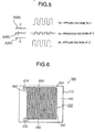
- FIG. 5 is a view for describing an operation of the capacitive acceleration sensor 50 shown in Fig. 4.
- X(55) electrodes, Y(56) electrodes, and Z(57) electrodes are connected in common, respectively, which can resultantly be considered as a circuit comprising two capacitors connected in series where the electrode X(55) is disposed between the electrodes Y(56) and Z(57) faced to each other as illustrated in Fig. 5.
- the mass M 5 represents the mass of the movable plate 54 including the movable electrodes 55(X).
- the movable electrodes 55(X) are displaced to positions where the balance is established with elastic force of the supporting portions 53 fixed to the anchors 52. Specifically, in Fig. 4, the movable electrodes 55(X) are shifted from the center position towards the fixed electrode 56(Y) or 57(Z).
- a metal thin film having resistance changing in response to the strain applied thereto is formed on a thin substrate, such as polyimide, by means of vapor deposition or the like.
- the thin substrate such as polymide must be adhered by the use of an adhesive to a plate to be subjected to detection of the strain. Since a detection characteristic will vary depending upon an adhering position or the fluctuation in thickness of an adhesive layer, the characteristic must be confirmed upon each adhesion.
- the flat plate is a metallic plate which is subjected to a deformation to be detected
- another metal plate is disposed to face the above-mentioned metallic plate to detect, as the change in capacitance between two electrodes, the change in spacing between the metal plates facing each other in response to the deformation of the metallic plate to be detected.
- this method it is necessary to accurately hold the positional relationship between the metallic plate to be detected and the other metal plate separately arranged. Therefore, the structure is complicated, resulting in difficulty in manufacturing.
- the strain gauge using a semiconductor is advantageous as the strain sensor because the sensitivity is as high as several ten times because of a piezo resistive effect, as compared with the strain gauge using the metal.
- the strain gauge using the semiconductor is disadvantageous in that the temperature-dependent change in resistance is large and the strain sensitivity varies with the strain level. Accordingly, if a small strain is measured, the structure becomes complicated.
- the piezoelectric type acceleration sensor described with reference to Fig. 3 is advantageous in that its structure is simple and no power supply is necessary in principle.
- an acceleration on a d.c. basis that is, a constant force is applied to a piezoelectric element
- electric charges produced by the deformation leak out through an electronic circuit for detection and a surface or an interior of a piezoelectric material so that the electric voltage is reduced. Consequently, it is difficult to correctly detect the applied acceleration.
- the movable electrode and the fixed electrode are required in order to establish the capacitance.
- the applied acceleration is at first converted into the change in spacing between the movable electrode and the fixed electrode and, as a result, converted into the change in capacitance. Accordingly, in order to accurately form the movable electrode and the fixed electrode, an expensive equipment capable of achieving a high working accuracy is required. Thus, this acceleration sensor is unfavorable.
- a strain sensor which is simple in structure and stable in characteristic, which can accurately detect very small strain, and which can carry out correction not only for the temperature but also for other environmental factor such as the humidity. It is a further object to provide a strain sensor which has an advantage of a capacitive acceleration sensor capable of detecting an acceleration on a d.c. basis and which can be used as an acceleration sensor capable of detecting the change in capacitance responsive to deformation of an elastic body when the acceleration is applied, without using two electrodes, that is, a movable electrode and a fixed electrode, but using a single element.
- a capacitive strain sensor comprises a substrate and at least one interdigital pair-electrode capacitor formed thereon.
- the substrate is an elastic member having a flat or a curved surface on which a dielectric film layer is formed with a substantially uniform thickness and made of a material having a dielectric constant changing in dependence upon the strain.
- the interdigital pair-electrode capacitor comprises at least a pair of electrodes which are formed on a surface of the substrate as parallel linear electrodes comprising a plurality of linear conductors and which are combined in an interdigital pattern.
- the capacitive strain sensor is incorporated as a capacitor element in the oscillator circuit so that the magnitude of the strain responsive to the deformation of the elastic body can be converted into the change in capacitance or impedance and, furthermore, can readily be converted into the change in frequency. Since a very small change can be extracted in the frequency after conversion, it is possible to easily and reliably detect even a slight change in strain.
- the capacitive strain sensor may have a structure in which a plate-like elastic body is a flat plate having a disk shape or a polygonal shape including a square and the interdigital pair-electrode capacitor is formed so that the linear electrodes as the digits of the fingers of the interdigital pattern are arranged in substantially concentric circles around the center of the flat plate.
- a plate-like elastic body is a flat plate having a disk shape or a polygonal shape including a square and the interdigital pair-electrode capacitor is formed so that the linear electrodes as the digits of the fingers of the interdigital pattern are arranged in substantially concentric circles around the center of the flat plate.
- the capacitive strain sensor is effectively used in detecting the change in internal pressure of the closed container by detecting the strain of the ends as the change in capacitance of the capacitors.
- the capacitive strain sensor according to this invention may be one wherein the elastic body is formed in a rectangular structure and the interdigital pair-electrode capacitor comprises linear conductors and has a capacitance by forming a pair of electrode patterns including a pair of common electrodes extending in parallel to two parallel sides of the rectangular elastic body and faced to each other and a plurality of linear electrodes inclined by about 45° with respect to an extending direction of the common electrodes and extending in parallel to one another to be alternately interposed as the digits of the interdigital pattern.
- the above-mentioned electrode patterns are suitable for a cylindrical structure in which the elastic body extends in one axis direction as a center axis and has an outer peripheral surface having a circular section.
- the interdigital pair-electrode capacitor has a capacitance by forming a pair of electrode patterns including a pair of common electrodes forming ring patterns around an outer peripheral surface of the cylindrical structure and faced to each other and a plurality of linear electrodes inclined by about 45° with respect to the center axis direction and spirally extending from the common electrodes in parallel to one another to be alternately interposed as the digits of the interdigital pattern.
- the above-mentioned capacitive strain sensor is effective in detecting the strain for torsion in both directions.
- the capacitive strain sensor according to this invention may be one wherein the elastic body has a flat plate shape and is provided with a fixed portion formed on one end thereof and having a structure for preventing production of the strain and that a single interdigital pair-electrode capacitor is formed on the surface of the elastic body except the fixed portion.
- the capacitive strain sensor further comprises a weight formed on the surface of the elastic body except the fixed portion of the elastic body to promote the bending of the elastic body. By adding the weight, it is possible to effectively detect an applied acceleration.
- the above-mentioned capacitive strain sensor has a simple structure and can form an LC oscillator circuit or an RC oscillator circuit.
- the change in output frequency of the oscillator circuit depending on the change in capacitance is very effective in accurately and exactly detecting a small strain level by voltage conversion.
- the capacitive strain sensor for this purpose, at least one of an interdigital pair-electrode capacitor arranged as a reference or a separately arranged capacitor is provided as a reference capacitor.
- the capacitance of the reference capacitor is used for correction in strain detection.
- the elastic body with one interdigital pair-electrode capacitor formed thereon is provided with a fixed portion formed on one end thereof and having a thickness such that the strain is hardly produced or having a fixed structure for preventing production of the strain.
- the reference capacitor including the reference interdigital pair-electrode capacitor is formed on the fixed portion. Accordingly, even if the strain is produced in the elastic body, the reference capacitance is unchanged.
- the reference capacitor may be formed on a fixed body separate from the elastic body.
- a capacitive strain sensor comprises a thick or thin dielectric film layer having a substantially uniform thickness, made of a material having a dielectric constant changing in dependence upon the strain, and formed as a substrate on a flat surface or a curved surface of a plate-like or a bar-like elastic body, and parallel linear electrodes comprising a plurality of linear conductors formed on its surface to form at least one interdigital pair-electrode capacitor.
- a pair of comb-shaped electrode patterns are formed by linear conductors on a dielectric film layer 120 formed on a surface of a rectangular flat-plate insulating sheet 110.
- the pair of electrode patterns comprise a linear common electrode 220 arranged to extend in parallel with and near to one of opposite long sides of the rectangular flat-plate insulating sheet 110 and having one end connected to a terminal 210, and another linear common electrode 240 arranged to extend in parallel with and near to the other of the opposite long sides of the insulating sheet 110 and having one end connected to a terminal 230.
- the linear common electrode 220 is provided with a plurality of linear electrodes 250 extending in a direction perpendicular to the extending direction thereof and the linear common electrode 240 is similarly provided with a plurality of linear electrodes 260 extending in a direction perpendicular to the extending direction thereof. These linear electrodes are arranged in parallel to be alternately interposed, respectively.
- the linear electrodes 250 and 260 are alternately arranged at a predetermined spacing from one another to extend in parallel to opposite short sides of the rectangular flat-plate insulating sheet 110, and are connected via the linear common electrodes 220 and 240 to the individual terminals 210 and 230, respectively.
- the interdigital pair-electrode capacitor 200 is formed.
- the rectangular flat-plate insulating sheet 110 be bent in a direction perpendicular to the extending direction of the linear electrodes 250 and 260.
- the mutual spacing between adjacent ones of the linear electrodes 250 and 260 is varied. Specifically, in case where the electrode surface is deformed in an expanding shape, a tensile strain is produced in the dielectric film layer 120 to widen the mutual spacing. In case where the electrode surface is deformed in a depressed shape, a compressive strain is produced in the dielectric film layer 120 to narrow the mutual spacing. Accordingly, the value of the capacitance between the terminals 210 and 230 is changed.
- the rectangular flat plate insulating sheet 110 is made of zirconia ceramics which is relatively excellent in flexibility.
- the dielectric film layer 120 formed on the surface thereof is made of a lead-based material which is typically used in a ceramic capacitor and has a high dielectric constant.
- the rectangular flat plate insulating sheet 110 with the dielectric film layer 120 and the interdigital pair-electrode capacitor 200 formed on the surface thereof is cut into a piece having suitable length. While it is supported at both end portions of the long sides, it is pressed at its center in a direction parallel to the short sides by the use of a knife-edged pressing plate, and the pressing force (g) - capacitance change rate (%) characteristic is measured. The result is shown in Fig. 8. It is noted here that the characteristic plotted with ⁇ marks in Fig. 8 shows the measured values in case where the back side of the electrode surface is pressed, while the characteristic plotted with ⁇ marks shows the measured values in case where the top side of the electrode surface is pressed.
- the value of the capacitance is increased with the increase of the pressing force, although the deformation is such that the mutual spacing of the electrodes is increased.
- the value of the capacitance is decreased with the increase of the pressing force, although the deformation is such that the mutual spacing of electrodes is decreased.
- the change in capacitance between the terminals 210 and 230 as the capacitor is greater than the change in capacitance simply depending on the change in mutual spacing of the electrodes.
- the linear electrodes 250 and 260 exhibit very slight variation in length.
- the mutual spacing between adjacent ones of the linear electrodes 250 and 260 is not substantially changed so that the value of capacitance between the terminals 210 and 230 is not substantially changed.
- the interdigital electrode pattern shown in the figure serves as a strain sensor excellent in sensitivity with respect to the deformation in an axial direction perpendicular to the linear electrodes extending in parallel but the sensitivity is significantly reduced with respect to the deformation in another axial direction perpendicular to the above-mentioned direction, that is, in a direction parallel to the linear electrodes.
- the strain sensor it is more effective to form the interdigital pair-electrode having a shape matching a strain distribution on the surface of an elastic body so that the strain sensor can efficiently detect the deformation strain on the surface of the elastic body which is deformed in a state with its periphery fixed.
- a strain sensor formed in the center area of the upper end 21 of the elastic body 20 which is the hollow cylindrical closed container as illustrated in Fig. 1.
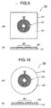
- the interdigital pair-electrode capacitor 200 shown in Fig. 6 is preferably rounded into an annular shape to form a circular-shaped interdigital pair-electrode capacitor 201 as illustrated in Figs. 9(A), 9(B), 10(A), and 10(B) or into a circular shape having rounded corners in which the corners of the square are rounded.
- a square-shaped flat plate insulating sheet 111 is provided with a dielectric film layer 121.
- a circular-shaped flat plate insulating sheet 112 is provided with a dielectric film layer 122.
- a circular-shaped interdigital pair-electrode capacitor 201 of a same shape is formed on the surface of each dielectric film layer.
- the flat plate insulating sheet 112 having a complete circular shape illustrated in Figs. 10(A) and 10(B) is suitable so as to efficiently detect the deformation of the upper end 21.
- One interdigital pair-electrode capacitor 203 forming a pair of electrode patterns comprises common electrodes 213 and 223 which are connected to a pair of terminals (not shown in the figure) of the capacitor and each of which is arranged to extend in parallel with and along opposite long sides of a rectangular insulating sheet 113.
- common electrodes 213 and 223 which are connected to a pair of terminals (not shown in the figure) of the capacitor and each of which is arranged to extend in parallel with and along opposite long sides of a rectangular insulating sheet 113.
- a plurality of linear electrodes 233 extending from the common electrode 213 and another plurality of linear electrodes 243 extending from the linear common electrode 223 extend in a direction approximately 45° with respect to the extending direction of the common electrodes 213 and 223 and are arranged to be alternately interposed in parallel to one another.
- one capacitor is formed.
- Fig. 12 is a perspective view showing a basic structure of one torsional strain sensor 104 according to this invention.
- the torsional strain sensor 104 shown in the figure is formed on an outer peripheral surface of an insulator bar 154.
- the insulator bar 154 is an object structure to be detected, which has one end fixed to a mount table 144, which extends therefrom with its center axis coincident with the center axis direction of the mount table 144, and which has a circular section across the outer peripheral surface.
- the material thereof is insulator plastics (or ceramics).
- a dielectric film layer 114 having a dielectric constant changing in dependence on the strain is formed on the outer peripheral surface of the insulator bar 154 to be substantially uniform in thickness, as a thick film or a thin film as a substrate of the torsional strain sensor 104.
- a pair of electrode patterns are formed by a pair of ring-shaped common electrodes 214 and 224 and a plurality of linear electrodes 234 and 244 in a spiral pattern to hold the capacitance.
- the pair of ring-shaped common electrodes 214 and 224 are arranged near two opposite sides parallel to each other, that is, along peripheral edges, respectively.
- the above-mentioned electrode patterns are characterized in that the plurality of linear electrodes 234 and 244 in a spiral pattern spirally extend from the pair of ring-shaped common electrodes 214 and 224 in parallel to one another to be inclined by about 45° with respect to the center axis direction, that is, with respect to an extending direction of the common electrodes 214 and 224 and to be alternately interposed.
- the common electrodes 214 and 224 are connected to terminals (not shown in the figure) for a capacitor.
- the pair of electrode patterns formed by the common electrode 214 and the linear electrodes 234 and by the other common electrode 224 and the other linear electrodes 244 act as the capacitor having the capacitance.
- the strain sensor 104 can be arranged directly on the insulator bar 154 to provide a structure having no adhesive layer. Therefore, it is possible to easily obtain a simple structure and the change in capacitance having a stable characteristic.
- the torsional strain can be decomposed into a tensile strain and a compressive strain in directions of +45° and -45° with respect to a torsional axis direction, respectively.
- the dielectric constant is varied in a direction in which the spiral linear electrodes 234 and 244 are faced to each other, depending on whether the torsional strain is positive or negative (direction of the torsion), so that the value of the capacitance between the terminals of the capacitor is varied. From this variation, it is possible to detect the magnitude of the produced torsional strain.
- the magnitude of the strain differs depending upon the direction of the strain. Therefore, it is possible to additionally provide with another strain sensor capable of detecting the strain in a reverse direction and to thereby detect by both sensors tensile strains increased in opposite directions, which are added together to thereby enable to more effectively improve the sensitivity.
- a cylindrical capacitive torsional strain sensor comprising two sets of pairs of linear electrodes in a spiral pattern for detecting the strain in reverse directions as mentioned above.
- a torsional strain sensor 105 illustrated in Fig. 13 is formed on an outer peripheral surface of an insulator bar 155, like in Fig. 12.
- the insulator bar 155 has one end fixed to a mount table 145, extends therefrom with its center axis coincident with the center axis direction of the mount table 145, and has a circular section across the outer peripheral surface.
- a dielectric film layer 115 having dielectric constant changing in dependence on the strain is formed on the outer peripheral surface of the insulator bar 155 as a thick film or a thin film to be a substrate substantially uniform in thickness.
- one interdigital pair-electrode capacitor of the torsional strain sensor 105 is divided on the outer peripheral surface of the dielectric film layer 115 into two equal parts by a plane perpendicular to the center axis direction so that a pair of common electrodes 215 and 225 and another pair of common electrodes 255 and 265, that is, two sets of ring-shaped common electrodes having a distance substantially equal to 1/2 of that shown in Fig. 12 are arranged on a dielectric film layer 125.
- a first set of pair of linear electrodes 235 and 245 are inclined by about +45° with respect to the extending direction of the above-mentioned common electrodes 215 and 225 to form a first interdigital pair-electrode while a second set of pair of linear electrodes 275 and 285 are inclined by about -45° with respect to the extending direction of the above-mentioned common electrodes 255 and 265 to form a second interdigital pair-electrode capacitor.
- the capacitors are formed by the two sets of the spiral linear electrodes perpendicular to each other and forming a pair of electrode patterns. Therefore, it is possible to detect an equivalent strain level with respect to an equivalent torsion in a reverse direction.
- a torsional strain sensor 106 illustrated in Fig. 14 is formed on an outer peripheral surface of an insulator bar 156, like in Fig. 12.
- the insulator bar 156 has one end fixed to a mount table 146, extends therefrom with its center axis coincident with the center axis direction of the mount table 146, and has a circular section across the outer peripheral surface.
- a dielectric film layer 116 having an dielectric constant changing in dependence on the strain is formed on the outer peripheral surface of the insulator bar 156 as a thick film or a thin film to serve as a substrate substantially uniform in thickness.
- one interdigital pair-electrode capacitor of the torsional strain sensor 106 is divided with respect to the outer peripheral surface of the dielectric film layer 116 into two equal parts by split lines parallel to the center axis direction so as to include a pair of common electrodes 216 and 226 and another pair of common electrodes 256 and 266, that is, two sets of pair of half-ring common electrodes arranged on the common ring-shaped lines and located near two opposite sides.
- one electrode pattern is formed by a plurality of linear electrodes 236 and 246 spirally extending from the pair of common electrodes 216 and 226 in parallel to one another to be alternately interposed and inclined by about +45° with respect to the center axis direction while the other electrode pattern is formed by a plurality of linear electrodes 276 and 286 spirally extending from the pair of common electrodes 256 and 266 in parallel to one another to be alternately interposed and inclined by about -45° with respect to the center axis direction.
- the capacitance is formed by each pair of the electrode patterns.
- the capacitive strain sensor described with reference to Fig. 8 and using a material having a great "strain - dielectric constant characteristic" has a simple structure and can readily form an LC oscillator circuit or an RC oscillator circuit to carry out frequency conversion so that a very small strain level can precisely be detected. Therefore, the above-mentioned sensor is very effective in practical use.
- an output of an oscillator circuit 401 is connected to one input of an operational amplifier 403 via an f-v (frequency-voltage) converter 402 and a resistance value R1.
- the ground and the feedback of an output of the operational amplifier 403 are connected to the other input of the operational amplifier 403 via the resistance value R1 and a resistance value R2, respectively.
- the oscillator circuit 401 shown in the figure has the above-mentioned interdigital pair-electrode capacitor of the capacitive strain sensor with the capacitance thereof incorporated into the LC circuit or the RC circuit. Accordingly, when the capacitance is varied due to the generation of the strain, an output frequency of the oscillator circuit 401 is changed. The change in frequency is converted into a voltage by the f-v converter 402. Through the operational amplifier 403, a very small strain level can be accurately detected.
- the capacitive strain sensor has a simple structure and can readily form the LC oscillator circuit or the RC oscillator circuit so that it is very effective in practical use.
- the capacitance varies also by the change in ambient temperature. Therefore, it is necessary to correct the capacitance change depending on the temperature.
- Fig. 16 is a perspective view showing a capacitive strain sensor 107 according to an embodiment of this invention.
- the capacitive strain sensor 107 shown in the figure comprises a ceramics substrate 117 having sections different in thickness and a dielectric layer 127 made of a material having a dielectric constant changing in dependence upon the strain and formed on a flat plane of the ceramic substrate.
- a thin portion of the substrate 117A suffers large strain.
- a thick portion of the substrate 117B is free from strain even if it is subjected to a large external pressure.
- the capacitive strain sensor 107 comprises two interdigital pair-electrode capacitors 207 and 207A having the same shape.
- the one interdigital pair-electrode capacitor 207 is formed on the surface of the substrate 117A while the other interdigital pair-electrode capacitor 207A is formed on the surface of the substrate 117B.
- the interdigital pair-electrode capacitor 207A formed on the thick portion of the substrate 117B forms a reference capacitor for temperature compensation.
- the interdigital pair-electrode capacitor 207A which serves as the reference capacitor has a temperature characteristic similar to that of the interdigital pair-electrode capacitor 207 of the capacitive strain sensor 107 which serves to detect the strain.
- the variation in capacitance of the interdigital pair-electrode capacitor 207 with respect to the change in ambient temperature is corrected by the use of the variation in capacitance of the interdigital pair-electrode capacitor 207A as the reference capacitor so as to obtain the variation in capacitance with respect to the change in strain under the external force.
- Fig. 17 is a circuit diagram for carrying out temperature compensation by the use of an impedance of the interdigital pair-electrode capacitor 207 in the capacitive strain sensor 107 illustrated in Fig. 16 and by the use of an impedance of the interdigital pair-electrode capacitor 207A as the reference capacitor.
- a capacitor 501 and a resistor 502 represent the capacitance and an internal resistance of the interdigital pair-electrode capacitor 207, respectively
- a capacitor 501A and a resistor 502A represent the capacitance and an internal resistance of the interdigital pair-electrode capacitor 207A, respectively.
- the interdigital pair-electrode capacitors 207 and 207A are substantially equivalent in temperature characteristic of the capacitance and internal resistance. Accordingly, respective impedances are extracted as voltage values from output terminals to derive the difference therebetween by the use of a comparator 503 so that the temperature compensation is carried out.
- Fig. 18 is a block diagram for carrying out temperature compensation.
- oscillator circuits equivalent in structure are formed to include LC circuits or RC circuits each incorporating the capacitance of an interdigital pair-electrode capacitor in a capacitive strain sensor.
- the oscillation frequency of one of the oscillators including the interdigital electrode capacitors is subjected to temperature compensation by the use of the oscillation frequency of the other as the reference.
- each of the oscillator circuits 411 and 411A is formed by provision of the LC circuit or the RC circuit using each of the two interdigital pair-electrode capacitors (for example, 207 and 207A) equivalent in structure in the capacitive strain sensor.
- the interdigital pair-electrode capacitor (207A) used in the one oscillator circuit 411A serves as the above-mentioned reference capacitor. Since the output frequency is changed when the capacitance is varied, outputs of the oscillator circuits 411 and 411 A are converted into electric voltages by f-v converters 412 and 412A, respectively. By making the difference therebetween by the use of a comparator 413, the temperature compensation is carried out.
- the dielectric film layer is described as the dielectric thick film having the high dielectric constant used in a ceramic capacitor or the like.
- these capacitors need not be formed on a common body surface but may be arranged at different positions under such a condition that the interdigital pair-electrode capacitor for detecting the strain and the reference capacitor are assumed to be within a same temperature environment. Since the dielectric is significantly affected by the temperature, description has been made exclusively for the temperature compensation. However, compensation is also possible for other environmental factors such as the humidity.
- an acceleration sensor which uses an interdigital pair-electrode capacitor having the shape illustrated in Fig. 6 as a capacitive strain sensor, which has an advantage of the acceleration sensor capable of detecting an acceleration on a d.c. basis, and which is capable of detecting the change in capacitance due to deformation of an elastic body subjected to acceleration, by a single element without using electrodes, such as a fixed electrode and a movable electrode.
- Fig. 19 is a perspective view showing an acceleration sensor according to an embodiment of this invention.
- the acceleration sensor shown in the figure comprises a zirconia substrate 118, a ferroelectric thick film layer 128 having dielectric constant changing in dependence on strain and being formed on the surface of the substrate with a substantially uniform thickness, and one interdigital pair-electrode capacitor 208 formed as a capacitance element at an approximate center of the thick film 128.
- the interdigital pair-electrode capacitor 208 comprises linear electrodes extending in a direction perpendicular to a direction of the strain produced by the acceleration to be detected and a pair of common electrodes connected to two terminals for input and output.
- the zirconia substrate 118 has one end fixed by a supporting/fixing block 318 and the other end to which a weight 328 is fixed.
- a weight 328 is fixed in the acceleration sensor illustrated in Fig. 19
- an acceleration ⁇ 8 is applied in a direction perpendicular to a flat plane of the zirconia substrate 118.
- the interdigital pair-electrode capacitor 208 as one capacitance element, the value of the capacitance between two terminals is changed. Since the capacitance is changed in proportion to the applied force, that is, the applied acceleration as illustrated in Fig. 8, it is possible to detect the applied acceleration from the change in capacitance.
- Fig. 20 is a perpendicular view showing an acceleration sensor according to another embodiment of this invention.
- the acceleration sensor shown in the figure comprises a zirconia substrate 119, a ferroelectric thick film layer 129 having a dielectric constant changing in dependence on strain and being formed on the surface of the substrate with a substantially uniform, and a first interdigital pair-electrode capacitor 209 formed as a capacitance element at an approximately center of the thick film 129.
- the first interdigital pair-electrode capacitor 209 is formed by an interdigital pair-electrode in which the linear electrodes extend in a direction perpendicular to a direction of the strain produced by the acceleration to be detected. Two terminals of the first interdigital pair-electrode capacitor 209 are led out for input and output from the respective linear electrodes via common electrodes.
- the zirconia substrate 119 has one end fixed to a supporting/fixing block 319 and the other end to which a weight 329 is fixed.
- a second interdigital pair-electrode capacitor 209A comprising linear electrodes equal in shape and size to the first interdigital pair-electrode capacitor 209 is formed as the capacitance element at a portion where the zirconia substrate 119 is fixed and adhered to the supporting/fixing block 319 and that the two terminals for input and output of the capacitance element are led out from the respective linear electrodes via the common electrodes.
- these interdigital pair-electrode capacitors 209 and 209A are formed on the ferroelectric thick film of the same material to be close to each other and are substantially identical in shape and size with each other. Accordingly, the capacitances of the respective interdigital pair-electrode capacitors are similarly affected by environmental conditions, such as the change in ambient temperature and electromagnetic noise, other than the acceleration.
- environmental conditions such as the change in ambient temperature and electromagnetic noise
- the capacitance obtained by the second interdigital pair-electrode capacitor additionally provided as one capacitance element can be used as the reference for detection of the acceleration.
- the common electrode of the interdigital pair-electrode capacitor has a linear shape.
- the shape is not limited to the linear shape but may be a narrow plate shape, a thin plate shape, a narrow and thin plate shape.
- the elastic body having a surface on which the strain sensor is formed has been described with reference to an example of a closed container having the top and the bottom surfaces which have a square shape or a circular shape.
- a closed container having the top and the bottom surfaces which have a square shape or a circular shape.
- the closed container has been mentioned as a cylindrical shape, this invention is applicable to any other shape as far as the shape has a plate member portion which is deformed in response to an internal pressure.
- the dielectric film layer is formed via an insulation layer having a low dielectric constant so that the capacitive strain sensor can readily be obtained with the same effect.
- the zirconia substrate is used as the insulator substrate and the ferroelectric layer is formed as a thick film.
- the insulator substrate may comprise a glass substrate or a Si single crystal substrate with SiO 2 film formed thereon and a ferroelectric thin film layer may be formed by sputtering or the like on the surface of the substrate.
- the acceleration sensor has a so-called cantilevered structure having one end as a fixed end, with the weight added to the distal end.
- the similar effect can be obtained with the structure in which both ends of a rectangular plate is fixed with a weight added at a center area.
- the substrate having a circular plate shape or a square plate shape is used, the similar effect is obtained by fixing its peripheral portion and adding the weight to the center.
- the same effect can be obtained.
- the substrate has a circular shape or a square shape
- the strain produced when the acceleration is applied in a direction perpendicular to the plate surface is produced in a substantially concentric pattern. Therefore, it is more effective that the interdigital electrode has a concentric pattern corresponding to the strain distribution.
- the mass of the substrate itself may be used as a weight without adding a special weight.
- a capacitive strain sensor is formed on the surface of the elastic body and detects the strain accompanying the bending of the elastic body with reference to the change in capacitance.
- the capacitive strain sensor is adapted to the use in a field in which the above-mentioned strain is produced.
- the capacitive strain sensor is incorporated as an element of an oscillator circuit so that the magnitude of the strain due to the deformation of the elastic body can be converted into the change in capacitance and, furthermore, can readily be converted into the change in frequency. Since the converted frequency can finely be extracted, it is possible to easily detect a slight change in strain.
- the strain sensor according to this invention is also suitable, for example, for detecting an internal pressure of a hollow-cylindrical closed container formed by the elastic body with reference to expansion/depression of a top plane portion, for detecting a cylinder torsion produced on an outer peripheral surface of a bar-like cylindrical elastic body, and as an acceleration sensor for detecting an acceleration.
Landscapes
- Physics & Mathematics (AREA)
- General Physics & Mathematics (AREA)
- Engineering & Computer Science (AREA)
- Power Engineering (AREA)
- Measuring Fluid Pressure (AREA)
- Measurement Of Length, Angles, Or The Like Using Electric Or Magnetic Means (AREA)
- Details Of Aerials (AREA)
- Force Measurement Appropriate To Specific Purposes (AREA)
Abstract
Description
Claims (25)
- A capacitive strain sensor comprising a substrate comprising an elastic body having at least one of a flat surface or a curved surface and a dielectric film layer formed on the surface with a substantially uniform thickness and made of a material having a dielectric constant changing in dependence upon strain, and at least one interdigital pair-electrode capacitor formed on the surface of said substrate, one capacitor comprising a pair of electrodes which are formed by a plurality of linear conductors as parallel linear electrodes and which are combined in an interdigital pattern.
- A capacitive strain sensor as claimed in claim 1, wherein each of at least two interdigital pair-electrode capacitors is formed so that each of said linear electrodes as digits of the interdigital pattern has a linear shape and that extending directions of said linear electrodes are substantially perpendicular to each other.
- A capacitive strain sensor as claimed in claim 1, wherein said plate-like elastic body has a shape of a flat plate as one of a circular plate or a polygonal plate including a square plate, said interdigital pair-electrode capacitor is formed so that said linear electrodes as digits of said interdigital pattern are arranged in substantially concentric circles with respect to the center of said flat plate.
- A capacitive strain sensor as claimed in claim 1, wherein said one elastic body has a rectangular structure, said interdigital pair-electrode capacitor comprising a pair of common electrodes extending in parallel to two parallel sides of said rectangular elastic body and faced to each other and said plurality of linear electrodes inclined by about 45° with respect to an extending direction of said common electrodes and extending in parallel to one another to be alternately interposed as digits of the interdigital pattern to form a pair of electrode patterns to thereby produce a capacitance.
- A capacitive strain sensor as claimed in claim 1, wherein said elastic body has a cylindrical structure which extends in one axis direction as a center axis and has a circular section across an outer peripheral surface, said dielectric film layer being formed on the outer peripheral surface of said cylindrical structure to be substantially uniform in thickness, said interdigital pair-electrode capacitor comprising a pair of electrode patterns including a pair of common electrodes forming ring patterns around the outer peripheral surface of said cylindrical structure and faced to each other and said plurality of linear electrodes inclined by about 45° with respect to the center axis direction and spirally extending from said common electrodes in parallel to one another to be alternately interposed as digits said interdigital pattern to thereby produce a capacitance.
- A capacitive strain sensor as claimed in claim 1, wherein said elastic body has a cylindrical structure which extends in one axis direction as a center axis and has a circular section across an outer peripheral surface, said dielectric film layer being formed on the outer peripheral surface of said cylindrical structure to be substantially uniform in thickness, said interdigital pair-electrode capacitor comprising at least two sets of electrode patterns arranged coaxial with said center axis so that the directions of digits in said interdigital patterns are different, said capacitor comprising, on one hand, a pair of first electrode patterns including a pair of common electrodes forming ring patterns around the outer peripheral surface of said cylindrical structure and faced to each other and a plurality of first linear electrodes inclined by about 45° with respect to the center axis direction and spirally extending from said common electrodes in parallel to one another to be alternately interposed, to thereby produce a capacitance, said capacitor, on the other hand, another pair of second electrode patterns including a pair of common electrodes forming ring patterns around the outer peripheral surface of said cylindrical structure and a plurality of second linear electrodes inclined substantially perpendicular to the extending direction of said first linear electrodes and spirally extending from said common electrodes in parallel to one another to be alternately interposed, to produce another capacitance.
- A capacitive strain sensor as claimed in claim 1, wherein said elastic body has a cylindrical structure which extends in one axis direction as a center axis and has a circular section across an outer peripheral surface, said dielectric film layer being formed on the outer peripheral surface of said cylindrical structure to be substantially uniform in thickness, said interdigital pair-electrode capacitor having two capacitances by forming two pair of electrode patterns including at least two sets of pair of half-ring common electrodes which are divided by split lines parallel to said center axis direction, arranged on common ring-shaped lines, and faced to each other with the directions of digits in said interdigital patterns are different, a plurality of first linear electrodes inclined by about 45° with respect to the center axis direction and spirally extending from said common electrodes in parallel to one another to be alternately interposed, and a plurality of second linear electrodes inclined substantially perpendicular to the extending direction of said first linear electrodes and spirally extending in parallel to one another to be alternately interposed.
- A capacitive strain sensor as claimed in claim 1, wherein said elastic body has a flat plate shape and has one end provided with a fixed portion having a structure for preventing generation of the strain, said interdigital pair-electrode capacitor being formed on the surface of said elastic body except said fixed portion.
- A capacitive strain sensor as claimed in claim 8, further comprising a weight formed on the surface of said elastic body except said fixed portion of said elastic body to promote the bending of said elastic body.
- A capacitive strain sensor as claimed in claim 1, wherein at least one of a plurality of said interdigital pair-electrode capacitors is selected as a reference interdigital pair-electrode capacitor.
- A capacitive strain sensor as claimed in claim 10, wherein said elastic body has one end provided with a fixed portion having at least one of a thickness hardly producing the strain and a structure preventing production of the strain, said reference interdigital pair-electrode capacitor being formed on said fixed portion.
- A capacitive strain sensor as claimed in claim 11, wherein said elastic body is provided with a fixed portion fixing the one end and a weight formed on the other end thereof to promote the bending of said elastic body, said reference interdigital pair-electrode capacitor being formed on said fixed portion.
- A capacitive strain sensor as claimed in claim 1, wherein one of an interdigital pair-electrode capacitor among said plurality of interdigital pair-electrode capacitors and a different capacitor element formed separately from the above-mentioned interdigital pair-electrode capacitors is selected as a reference capacitor.
- A capacitive strain sensor as claimed in claim 13, wherein said elastic body has one end provided with a fixed portion having at least one of a thickness hardly producing the strain and a structure preventing production of the strain, said capacitor being formed on said fixed portion.
- A capacitive strain sensor as claimed in claim 13, wherein said reference capacitor is formed on a fixed part disposed separately from said elastic body.
- A capacitive strain sensor as claimed in claim 1, wherein any one of insulating plastics, a single crystal, and ceramics is used as a material of said elastic body.
- A capacitive strain sensor as claimed in claim 1, wherein a conductor is used as a material of said elastic body, said conductor having a surface previously provided with an insulating layer made of either of plastics and ceramics having a low dielectric constant, said interdigital pair-electrode capacitor being formed on a surface of said insulating layer.
- A method of using a capacitive strain sensor claimed in claim 1, wherein said elastic body is one of a top end or a bottom end of a cylindrical closed container, said interdigital pair-electrode capacitor detecting the change in internal pressure of said closed container by detecting a strain of said flat end produced on said flat end as a change in the capacitance of said capacitor.
- A method of using a capacitive strain sensor claimed in claim 1, wherein said elastic body has a cylindrical structure which extends in one axis direction as a center axis and has a circular section across an outer peripheral surface, said dielectric film layer being formed on the outer peripheral surface of said cylindrical structure with a substantially uniform thickness, said interdigital pair-electrode capacitor comprising a pair of electrode patterns comprising a pair of common electrodes forming ring patterns around the outer peripheral surface of said cylindrical structure and faced to each other and said plurality of linear electrodes inclined by about 45° with respect to the center axis direction and spirally extending from said common electrodes in parallel to one another to be alternately interposed as digits of said interdigital pattern to thereby produce a capacitance, the torsional strain of said cylindrical structure being detected as a change in the capacitance of said capacitor.
- A method of using a capacitive strain sensor as claimed in claim 1, wherein said elastic body has a cylindrical structure which extends in one axis direction as a center axis and has a circular section across an outer peripheral surface, said cylindrical structure having one of a ring shape, a columnar shape, a cylindrical shape, and a bar shape, said capacitive strain sensor being formed on the outer peripheral surface of said cylindrical structure, torsional strain of said cylindrical structure being detected as a change in the capacitance of said capacitive strain sensor.
- A method of using a capacitive strain sensor claimed in claim 1, wherein said elastic body has a flat plate shape and has one end provided with a fixed portion and having a structure for preventing generation of the strain, said interdigital pair-electrode capacitor being formed on the surface of said elastic body except said fixed portion, the applied acceleration being detected as a change in the capacitance of said interdigital pair-electrode capacitor due to deformation of said elastic body as a result of the acceleration applied thereto.
- A method of using a capacitive strain sensor as claimed in claim 1, wherein provision is made of oscillation means for generating frequency modulation corresponding to a change in capacitance of said capacitive strain sensor, the strain level being detected as a fluctuation in frequency of an oscillation signal produced by said oscillation means.
- A method of using a capacitive strain sensor as claimed in claim 1, wherein one of an interditigal pair-electrode capacitor among said plurality of interdigital pair-electrode capacitors and a different capacitor element formed separately from the above-mentioned interdigital pair-electrode capacitors is selected as a reference capacitor, a capacitance of said reference capacitor being used for compensating a variation in capacitance of the remaining interdigital pair-electrode capacitors.
- A method of using a capacitive strain sensor claimed in claim 1, wherein one of an interditigal pair-electrode capacitor among said plurality of interdigital pair-electrode capacitors and a different capacitor element formed separately from the above-mentioned interdigital pair-electrode capacitors is selected as a reference capacitor, a variation in impedance between said reference capacitor and the remaining interdigital pair-electrode capacitors being used for compensating the strain detected.
- A method of using a capacitive strain sensor claimed in claim 1, wherein at least one of an interditigal pair-electrode capacitor among said plurality of interdigital pair-electrode capacitors and a different capacitor element formed separately from the above-mentioned interdigital pair-electrode capacitors is selected as a reference capacitor, oscillator circuits being formed by incorporating either of an inductance (L) and an resistance (R) with the capacitance (C) of each of said reference capacitor and the remaining interdigital pair-electrode capacitors, respectively, a variation between an oscillation frequency output of the oscillator circuit including said reference capacitor and an oscillation frequency output of the other oscillator circuit including each of said remaining interdigital pair-electrode capacitors being used for compensating a strain detected.
Applications Claiming Priority (11)
| Application Number | Priority Date | Filing Date | Title |
|---|---|---|---|
| JP19600399 | 1999-07-09 | ||
| JP11196003A JP2001021308A (en) | 1999-07-09 | 1999-07-09 | Capacitive strain sensor |
| JP24887699 | 1999-09-02 | ||
| JP24851699 | 1999-09-02 | ||
| JP24851699A JP2001074569A (en) | 1999-09-02 | 1999-09-02 | Flat-plate capacitive torsional strain sensor |
| JP24887699A JP4242977B2 (en) | 1999-09-02 | 1999-09-02 | Cylindrical capacitive torsional strain sensor |
| JP26021899 | 1999-09-14 | ||
| JP26021899A JP4394212B2 (en) | 1999-09-14 | 1999-09-14 | Acceleration sensor |
| JP26182399A JP2001082909A (en) | 1999-09-16 | 1999-09-16 | Capacitive strain sensor |
| JP26182399 | 1999-09-16 | ||
| PCT/JP2000/004538 WO2001004593A1 (en) | 1999-07-09 | 2000-07-07 | Capacitive strain sensor and method for using the same |
Publications (2)
| Publication Number | Publication Date |
|---|---|
| EP1113252A1 true EP1113252A1 (en) | 2001-07-04 |
| EP1113252A4 EP1113252A4 (en) | 2001-09-19 |
Family
ID=27529135
Family Applications (1)
| Application Number | Title | Priority Date | Filing Date |
|---|---|---|---|
| EP00944327A Withdrawn EP1113252A4 (en) | 1999-07-09 | 2000-07-07 | Capacitive strain sensor and method for using the same |
Country Status (6)
| Country | Link |
|---|---|
| US (1) | US6532824B1 (en) |
| EP (1) | EP1113252A4 (en) |
| KR (1) | KR100421304B1 (en) |
| CN (1) | CN1157594C (en) |
| TW (1) | TW432198B (en) |
| WO (1) | WO2001004593A1 (en) |
Cited By (9)
| Publication number | Priority date | Publication date | Assignee | Title |
|---|---|---|---|---|
| DE19961299B4 (en) * | 1999-12-18 | 2009-04-30 | Robert Bosch Gmbh | Sensor for detecting knocking in an internal combustion engine |
| US7545119B1 (en) | 2008-07-31 | 2009-06-09 | International Business Machines Corporation | Sensor incorporated into energy storage device package |
| EP1773186A4 (en) * | 2004-07-08 | 2009-08-12 | Deborah Schenberger | Strain monitoring system and apparatus |
| EP2037249A3 (en) * | 2007-09-17 | 2014-05-28 | Liebherr-Werk Nenzing GmbH | Device for measuring mechanical parameters, method for measuring mechanical parameters and use of a device for measuring mechanical parameters |
| DE10360309B4 (en) * | 2003-12-18 | 2015-01-22 | Horst Ahlers | Resistive strain sensor |
| KR20160035144A (en) * | 2014-09-22 | 2016-03-31 | 한국과학기술원 | A sensing technique based on dielectric changes in metal capacitor |
| EP3009822A1 (en) * | 2014-10-16 | 2016-04-20 | Nokia Technologies OY | A deformable apparatus and method |
| US10435289B2 (en) | 2014-10-16 | 2019-10-08 | Nokia Technoloiges Oy | Deformable apparatus and method |
| WO2023111344A1 (en) * | 2021-12-17 | 2023-06-22 | Nanomade Lab | Microsensor with interdigitated electrodes |
Families Citing this family (102)
| Publication number | Priority date | Publication date | Assignee | Title |
|---|---|---|---|---|
| AU2001223397A1 (en) * | 2000-02-01 | 2001-08-14 | Disetronic Licensing Ag | Configurable device and method for releasing a substance |
| AU2001223396A1 (en) * | 2000-02-01 | 2001-08-14 | Disetronic Licensing Ag | Container and device for administering a substance |
| US6518083B2 (en) * | 2001-01-31 | 2003-02-11 | Nippon Telegraph And Telephone Corporation | Surface shape recognition sensor and method of manufacturing the same |
| DE10139158C1 (en) * | 2001-08-09 | 2003-04-17 | Siemens Dematic Ag | Component detection device, component supply device and method for supplying components by means of a component supply device |
| ATE485763T1 (en) * | 2002-12-14 | 2010-11-15 | Univ Tsinghua Res Inst | APPARATUS AND METHOD FOR MONITORING THE COMPOSITION OF THE BODY BY DETERMINING THE DIELECTRICITY CONSTANT AND THE IMPEDANCE OF THE BODY BASED ON DIGITAL FREQUENCY SENSING |
| JP2007526994A (en) * | 2003-08-12 | 2007-09-20 | ジュン パク,フン | Load measuring transducer including elastic structure and gauge using induced voltage, and load measuring system using the transducer |
| GB0323781D0 (en) * | 2003-10-10 | 2003-11-12 | Bodycage Ltd | Safety helmet |
| US7644628B2 (en) * | 2005-12-16 | 2010-01-12 | Loadstar Sensors, Inc. | Resistive force sensing device and method with an advanced communication interface |
| US20060030062A1 (en) * | 2004-08-05 | 2006-02-09 | Jun He | Micromachined wafer strain gauge |
| US7204162B2 (en) * | 2004-11-23 | 2007-04-17 | Delphi Technologies, Inc. | Capacitive strain gauge |
| DE102005002057B4 (en) * | 2005-01-14 | 2007-05-31 | Nicol, Klaus, Prof. Dr. | Sensor for measuring the distribution of a surface pressure |
| US7509870B2 (en) * | 2005-10-26 | 2009-03-31 | Orthodata Technologies Llc | MEMS capacitive bending and axial strain sensor |
| US7728492B2 (en) | 2005-12-19 | 2010-06-01 | Physical Logic Ag | Piezoelectric composite material |
| US8104358B1 (en) * | 2006-01-23 | 2012-01-31 | University Of Puerto Rico | High sensitivity passive wireless strain sensor |
| JP2008089412A (en) * | 2006-10-02 | 2008-04-17 | Matsushita Electric Works Ltd | Pressure sensor |
| DE112008000578B4 (en) * | 2007-03-23 | 2014-05-22 | Murata Mfg. Co., Ltd. | Antenna and radio communication device |
| EP2065681A1 (en) * | 2007-11-30 | 2009-06-03 | Paramata Limited | Sensing system and method |
| US20090158856A1 (en) * | 2007-12-23 | 2009-06-25 | Divyasimha Harish | Capacitive strain gauge system and method |
| US20090229369A1 (en) * | 2008-03-17 | 2009-09-17 | Siew-Seong Tan | Capacitor Compensation Structure and Method for a Micro-Electro-Mechanical System |
| US7784366B2 (en) * | 2008-07-29 | 2010-08-31 | Motorola, Inc. | Single sided capacitive force sensor for electronic devices |
| US8342031B2 (en) * | 2008-10-27 | 2013-01-01 | The Regents Of The University Of California | Capacitive strain sensor |
| US8225677B2 (en) * | 2008-11-06 | 2012-07-24 | Northeastern University | Capacitive sensor, system, and method for measuring parameters of a two-phase flow |
| US8564310B2 (en) * | 2009-08-18 | 2013-10-22 | 3M Innovative Properties Company | Capacitive oil quality monitoring sensor with fluorinated barrier coating |
| KR101085489B1 (en) | 2009-10-16 | 2011-11-21 | 박흥준 | Load measuring transducer using induced voltage to compensate for errors caused by temperature and load measuring system using the transducer |
| CN102062652A (en) * | 2009-11-12 | 2011-05-18 | 无锡千里信步精密机电科技有限公司 | Pressure sensor device using flexible inducting material mixed with micro construction bodies and pressure signal inducting method |
| US8633916B2 (en) | 2009-12-10 | 2014-01-21 | Apple, Inc. | Touch pad with force sensors and actuator feedback |
| US9018060B2 (en) | 2010-06-15 | 2015-04-28 | 3M Innovative Properties Company | Variable capacitance sensors and methods of making the same |
| DE102011078557A1 (en) | 2011-07-01 | 2013-01-03 | Endress + Hauser Gmbh + Co. Kg | Method for operating an absolute or relative pressure sensor with a capacitive transducer |
| DE102012005262B4 (en) | 2012-03-15 | 2014-11-06 | Forschungszentrum Jülich GmbH | Sensor arrangement of carrier substrate and ferroelectric layer |
| KR101480752B1 (en) * | 2012-03-30 | 2015-01-09 | 한국과학기술원 | Apparatus for measuring surface shape |
| RU2507474C1 (en) * | 2012-08-07 | 2014-02-20 | Открытое акционерное общество "Авангард" | Induction position sensor |
| US9250143B2 (en) * | 2012-09-19 | 2016-02-02 | College Park Industries, Inc. | Multicapacitor force/moment sensor arrays |
| CN102980508A (en) * | 2012-11-21 | 2013-03-20 | 昆山北极光电子科技有限公司 | Auto-balancing mechanical deformation measuring method |
| CN102997834B (en) * | 2012-12-12 | 2016-05-25 | 山东建筑大学 | A kind of non-conductive medium film thickness on-line measuring device of coplanar capacitance sensor |
| CN104034251B (en) * | 2013-03-06 | 2016-12-28 | 中国科学院合肥物质科学研究院 | A kind of micro-meter scale material strain detection device and detection method thereof |
| DE102013114734A1 (en) * | 2013-12-20 | 2015-07-09 | Endress + Hauser Gmbh + Co. Kg | Capacitive pressure cell with at least one temperature sensor and pressure measuring method |
| JP6364886B2 (en) * | 2014-03-31 | 2018-08-01 | 大日本印刷株式会社 | Method for detecting deformation of packaging bag |
| CA2901026C (en) | 2014-08-19 | 2020-11-24 | Western Michigan University Research Foundation | Helmet impact monitoring system |
| EP3211364B1 (en) * | 2014-10-22 | 2020-02-19 | Bando Chemical Industries, Ltd. | Capacitance sensor |
| CN105720964A (en) * | 2014-12-02 | 2016-06-29 | 天津富纳源创科技有限公司 | Pressure detection button, controller and pressure detection button operation method |
| KR101739791B1 (en) * | 2015-05-11 | 2017-05-26 | 주식회사 하이딥 | Pressure sensor, pressure detector and touch input device including the same |
| CN105021120B (en) * | 2015-07-06 | 2019-07-19 | 电子科技大学 | A capacitive strain sensor and method of making the same |
| CN105180793B (en) * | 2015-08-13 | 2017-07-25 | 浙江工业大学 | It can measure the lateral deflection of the lateral deflection of the surface strain, the full bridge and the interdigitated metal strain gauge |
| CN105066870B (en) * | 2015-08-13 | 2017-09-22 | 浙江工业大学 | The double interdigitated metal foil gauges of axial deviation full-bridge of the axial local derviation of measurable surface strain |
| US10067007B2 (en) * | 2015-09-02 | 2018-09-04 | Oculus Vr, Llc | Resistive-capacitive deformation sensor |
| US9666661B2 (en) * | 2015-09-08 | 2017-05-30 | Taiwan Semiconductor Manufacturing Company, Ltd. | Coplanar metal-insulator-metal capacitive structure |
| US10732055B2 (en) * | 2015-10-30 | 2020-08-04 | Northwestern University | Dielectrostrictive sensors for shear stress measurement, process monitoring, and quality examination of viscoelastic materials |
| CN105241585B (en) * | 2015-11-12 | 2017-08-18 | 桂林电子科技大学 | A kind of capacitive sensor device based on silver conductive adhesive and preparation method thereof |
| CN105423906B (en) * | 2015-12-04 | 2017-12-05 | 浙江工业大学 | The interdigital metal strain plate in sensitive grid side of cross direction profiles five of horizontal local derviation outside measurable unilateral piece |
| CN105423900B (en) * | 2015-12-04 | 2017-12-05 | 浙江工业大学 | Six sensitive grid full-bridge of cross direction profiles, the three interdigital metal strain plate of horizontal local derviation outside measurable unilateral piece |
| CN105547133B (en) * | 2015-12-04 | 2017-12-05 | 浙江工业大学 | The five interdigital metal strain plates in sensitive grid side of axial direction distribution of axial local derviation outside measurable unilateral piece |
| CN105547531B (en) * | 2016-01-19 | 2018-07-06 | 东南大学 | A kind of highly sensitive capacitance pressure transducer, and preparation method thereof |
| US10842667B2 (en) * | 2016-02-17 | 2020-11-24 | Tramec Termico Technologies, L.L.C. | Self-regulating heater |
| CN105823411B (en) * | 2016-03-18 | 2019-02-22 | 苏州椒图电子有限公司 | A kind of curved surface profile measurement method |
| CN106092430B (en) * | 2016-06-16 | 2018-11-16 | 清华大学深圳研究生院 | A kind of comb capacitance type pressure sensor |
| CN106247920B (en) * | 2016-07-07 | 2019-02-12 | 中国计量大学 | A Surface Strain Detection Device Based on Elastic Substrate Sandwich Interdigital Capacitance |
| US10637108B1 (en) | 2016-12-09 | 2020-04-28 | Cornell Dubilier Marketing, Inc. | Apparatus for detecting expansion of an energy storage device case |
| US10612991B1 (en) * | 2017-08-25 | 2020-04-07 | Fluke Corporation | High dynamic range capacitive pressure sensor |
| JP6988469B2 (en) | 2017-12-27 | 2022-01-05 | 株式会社デンソー | Strain detection device and diagnostic device using it |
| CN108414126A (en) * | 2018-01-22 | 2018-08-17 | 江苏军物联网股份有限公司 | A kind of welding post pressure monitor system and monitoring method |
| TWI659217B (en) * | 2018-03-27 | 2019-05-11 | 國立交通大學 | Wireless passive strain sensor |
| AT521182B1 (en) * | 2018-07-11 | 2019-11-15 | Greenwood Power Og | Voltage dividing device with rod structure |
| CN109238519B (en) * | 2018-10-22 | 2024-03-15 | 河北工业大学 | Hybrid flexible touch sensor |
| US11189536B2 (en) | 2018-12-31 | 2021-11-30 | Micron Technology, Inc. | Method and apparatus for on-chip stress detection |
| CN109786430B (en) * | 2019-02-22 | 2021-01-26 | 京东方科技集团股份有限公司 | Flexible display panel and display device |
| JP7272836B2 (en) * | 2019-03-19 | 2023-05-12 | 住友重機械工業株式会社 | Sensor, sensor fixing structure |
| CN109883316B (en) * | 2019-03-22 | 2021-01-29 | 中国科学院力学研究所 | A resistive strain sensor and strain measurement method |
| US11021950B2 (en) * | 2019-06-06 | 2021-06-01 | Probe Technology Services, Inc. | Production-logging sensor |
| CA3083837A1 (en) | 2019-06-12 | 2020-12-12 | The Board Of Trustees Of Western Michigan University | Pressure monitoring system for helmets |
| US11762517B2 (en) * | 2019-06-19 | 2023-09-19 | Nissha Co., Ltd. | Touch panel |
| US11494147B2 (en) | 2019-06-26 | 2022-11-08 | Microsoft Technology Licensing, Llc | Sensing bending of multiple joints |
| CN110487168B (en) * | 2019-08-29 | 2024-03-01 | 清华大学深圳研究生院 | Unidirectional bending sensitive sensor and preparation method thereof |
| CN111189563B (en) * | 2020-01-07 | 2021-08-10 | 西安电子科技大学 | Pressure detection device and system |
| US11662820B2 (en) | 2020-01-08 | 2023-05-30 | Dell Products, Lp | System for a solid-state keyboard and touchpad providing haptic feedback |
| JP2021110703A (en) * | 2020-01-15 | 2021-08-02 | ミネベアミツミ株式会社 | Strain gauge |
| US11106772B2 (en) | 2020-01-31 | 2021-08-31 | Dell Products, Lp | System and method for continuous user identification via piezo haptic keyboard and touchpad dynamics |
| US11079816B1 (en) | 2020-01-31 | 2021-08-03 | Dell Products, Lp | System and method for vapor chamber directional heat dissipation for a piezoelectric keyboard assembly |
| US11067269B1 (en) | 2020-01-31 | 2021-07-20 | Dell Products, Lp | System and method for backlight integration with electrical contact foil in piezoelectric haptic keyboard |
| US11579695B2 (en) | 2020-01-31 | 2023-02-14 | Dell Products, Lp | System and method for generating sound effects on fingertips with piezoelectric actuators of a haptic keyboard |
| US10860112B1 (en) | 2020-01-31 | 2020-12-08 | Dell Products, Lp | System for a solid-state keyboard and touchpad with a single sheet cover for providing haptic feedback |
| US11093048B1 (en) | 2020-01-31 | 2021-08-17 | Dell Products, Lp | System for modified key actions and haptic feedback for smart typing assist with a solid-state keyboard and touchpad |
| US11079849B1 (en) | 2020-01-31 | 2021-08-03 | Dell Products, Lp | System for extended key actions and haptic feedback and optimized key layout for a solid-state keyboard and touchpad |
| US11106286B2 (en) | 2020-01-31 | 2021-08-31 | Dell Products, Lp | System and method for mood detection via piezo haptic keyboard dynamics |
| US11175745B2 (en) | 2020-01-31 | 2021-11-16 | Dell Products, Lp | System and method for application of piezo electric haptic keyboard personal typing profile |
| US10936073B1 (en) | 2020-01-31 | 2021-03-02 | Dell Products, Lp | System and method for generating high-frequency and mid-frequency audible sound via piezoelectric actuators of a haptic keyboard |
| US11301053B2 (en) | 2020-01-31 | 2022-04-12 | Dell Products, Lp | System for providing haptic feedback across full palm rest in fixed position of information handling system |
| US11294469B2 (en) | 2020-01-31 | 2022-04-05 | Dell Products, Lp | System and method for processing user input via a reconfigurable haptic interface assembly for displaying a modified keyboard configuration |
| US20210247218A1 (en) * | 2020-02-10 | 2021-08-12 | Hutchinson Technology Incorporated | Systems And Methods To Increase Sensor Robustness |
| CN111208317B (en) * | 2020-02-26 | 2021-07-02 | 深迪半导体(绍兴)有限公司 | MEMS inertial sensor, application method and electronic equipment |
| US11415538B2 (en) * | 2020-03-06 | 2022-08-16 | Applied Materials, Inc. | Capacitive sensor housing for chamber condition monitoring |
| WO2021188708A1 (en) | 2020-03-17 | 2021-09-23 | Arris Enterprises Llc | Ceramic based strain detector |
| JP7402148B2 (en) * | 2020-03-24 | 2023-12-20 | ミネベアミツミ株式会社 | strain gauge |
| CN111664968A (en) * | 2020-07-15 | 2020-09-15 | 襄阳臻芯传感科技有限公司 | Method for manufacturing ceramic capacitive pressure sensor |
| CN113340476B (en) * | 2021-05-08 | 2023-10-27 | 昆山朗德森机电科技有限公司 | A two-dimensional decoupled torque tactile sensor and MEMS preparation method |
| CN115598732B (en) * | 2021-07-08 | 2026-03-20 | 中国石油化工股份有限公司 | A Buried Hill Structure Identification Method Based on the Fusion of Gravity, Magnetic and Electrostatic Exploration Technologies |
| FR3126776B1 (en) * | 2021-09-09 | 2024-02-16 | Faurecia Sieges Dautomobile | Coplanar Interdigitated Electrode Capacitive Transducer, Vehicle Seat Occupancy Sensing Mat and Vehicle Seat |
| CN114111697B (en) * | 2021-11-26 | 2023-07-25 | 中国电建集团成都勘测设计研究院有限公司 | Monitoring and early warning device and monitoring and early warning method for toppling deformation body |
| CN114353916A (en) * | 2022-01-10 | 2022-04-15 | 江苏大学 | Quality measuring device based on flexible capacitive sensor |
| EP4500108A4 (en) * | 2022-03-29 | 2026-04-08 | Univ Carnegie Mellon | FLEXIBLE STRETCH SENSOR IN THE MICRO SCALE |
| CN114894859B (en) * | 2022-04-28 | 2025-09-09 | 兰州理工大学 | Welding rod humidity measuring device and method based on interdigital capacitive sensor |
| CN116448286B (en) * | 2022-10-10 | 2025-08-01 | 成都凯天电子股份有限公司 | Silicon resonance pressure sensor and online calibration method thereof |
| US12429392B2 (en) | 2023-03-03 | 2025-09-30 | STMicroloelectronics International N.V. | Linear capacitive pressure sensor |
Family Cites Families (18)
| Publication number | Priority date | Publication date | Assignee | Title |
|---|---|---|---|---|
| JPS5434519B2 (en) * | 1973-08-31 | 1979-10-27 | ||
| US4188651A (en) * | 1978-03-27 | 1980-02-12 | Sprague Electric Company | Ceramic capacitor with surface electrodes |
| US4520885A (en) * | 1981-08-05 | 1985-06-04 | Yoshida Kogyo K.K. | Load sensing apparatus with capacitive and inductive sensors |
| US4422127A (en) * | 1981-12-15 | 1983-12-20 | Electronic Concepts, Inc. | Substantially small sized wound capacitor and manufacturing method therefor |
| JPS5954904A (en) * | 1982-09-24 | 1984-03-29 | Hitachi Ltd | capacitive strain gauge |
| US4479392A (en) * | 1983-01-03 | 1984-10-30 | Illinois Tool Works Inc. | Force transducer |
| DE3634855C1 (en) * | 1986-10-13 | 1988-03-31 | Peter Seitz | Capacitive measuring arrangement for the determination of forces and / or pressures |
| ES2028421T3 (en) | 1988-08-11 | 1992-07-01 | Siemens Aktiengesellschaft | PRECEPTOR OF THE MEASURED VALUE FOR LENGTH OR DISTANCE VARIATIONS, ESPECIALLY FOR THE MEASUREMENT WITHOUT PHYSICAL CONTACT OF TURNING MOMENTS IN ROTATING TREES. |
| US5233213A (en) * | 1990-07-14 | 1993-08-03 | Robert Bosch Gmbh | Silicon-mass angular acceleration sensor |
| CH685214A5 (en) * | 1991-10-15 | 1995-04-28 | Hans Ulrich Meyer | capacitive sensor position. |
| US5608246A (en) * | 1994-02-10 | 1997-03-04 | Ramtron International Corporation | Integration of high value capacitor with ferroelectric memory |
| EP0776467B1 (en) | 1994-08-16 | 2000-05-10 | Siemens Aktiengesellschaft | Force or extension sensor |
| EP0776466B1 (en) * | 1994-08-16 | 1999-03-10 | Siemens Aktiengesellschaft | Force or extension sensor |
| FR2732467B1 (en) | 1995-02-10 | 1999-09-17 | Bosch Gmbh Robert | ACCELERATION SENSOR AND METHOD FOR MANUFACTURING SUCH A SENSOR |
| US5610528A (en) * | 1995-06-28 | 1997-03-11 | International Business Machines Corporation | Capacitive bend sensor |
| JP3525400B2 (en) * | 1995-10-17 | 2004-05-10 | Necトーキン株式会社 | Force detector |
| US5804065A (en) * | 1995-11-17 | 1998-09-08 | The United States Of America As Represented By The Secretary Of Agriculture | Control apparatus for marine animals |
| US6222376B1 (en) * | 1999-01-16 | 2001-04-24 | Honeywell International Inc. | Capacitive moisture detector and method of making the same |
-
2000
- 2000-07-07 WO PCT/JP2000/004538 patent/WO2001004593A1/en not_active Ceased
- 2000-07-07 KR KR10-2001-7002948A patent/KR100421304B1/en not_active Expired - Fee Related
- 2000-07-07 US US09/786,944 patent/US6532824B1/en not_active Expired - Fee Related
- 2000-07-07 TW TW089113557A patent/TW432198B/en not_active IP Right Cessation
- 2000-07-07 CN CNB008018863A patent/CN1157594C/en not_active Expired - Fee Related
- 2000-07-07 EP EP00944327A patent/EP1113252A4/en not_active Withdrawn
Cited By (21)
| Publication number | Priority date | Publication date | Assignee | Title |
|---|---|---|---|---|
| DE19961299B4 (en) * | 1999-12-18 | 2009-04-30 | Robert Bosch Gmbh | Sensor for detecting knocking in an internal combustion engine |
| DE10360309B4 (en) * | 2003-12-18 | 2015-01-22 | Horst Ahlers | Resistive strain sensor |
| US9060743B2 (en) | 2004-07-08 | 2015-06-23 | Deborah Munro | Strain monitoring system and apparatus |
| US9510785B2 (en) | 2004-07-08 | 2016-12-06 | Deborah Munro | Strain monitoring system and apparatus |
| US8070695B2 (en) | 2004-07-08 | 2011-12-06 | Deborah Schenberger | Strain monitoring system and apparatus |
| US8529474B2 (en) | 2004-07-08 | 2013-09-10 | Deborah Schenberger | Strain monitoring system and apparatus |
| US8622936B2 (en) | 2004-07-08 | 2014-01-07 | Deborah Schenberger (Munro) | Strain monitoring system and apparatus |
| US8721570B2 (en) | 2004-07-08 | 2014-05-13 | Deborah Munro (Schenberger) | Strain monitoring system and apparatus |
| US8066650B2 (en) | 2004-07-08 | 2011-11-29 | Deborah Schenberger | Strain monitoring system and apparatus |
| EP1773186A4 (en) * | 2004-07-08 | 2009-08-12 | Deborah Schenberger | Strain monitoring system and apparatus |
| EP2037249A3 (en) * | 2007-09-17 | 2014-05-28 | Liebherr-Werk Nenzing GmbH | Device for measuring mechanical parameters, method for measuring mechanical parameters and use of a device for measuring mechanical parameters |
| US7545119B1 (en) | 2008-07-31 | 2009-06-09 | International Business Machines Corporation | Sensor incorporated into energy storage device package |
| KR20160035144A (en) * | 2014-09-22 | 2016-03-31 | 한국과학기술원 | A sensing technique based on dielectric changes in metal capacitor |
| KR101665187B1 (en) | 2014-09-22 | 2016-10-13 | 한국과학기술원 | A sensing technique based on dielectric changes in metal capacitor |
| EP3009822A1 (en) * | 2014-10-16 | 2016-04-20 | Nokia Technologies OY | A deformable apparatus and method |
| WO2016059288A1 (en) * | 2014-10-16 | 2016-04-21 | Nokia Technologies Oy | A deformable apparatus and method |
| US10393599B2 (en) | 2014-10-16 | 2019-08-27 | Nokia Technologies Oy | Deformable apparatus and method |
| US10435289B2 (en) | 2014-10-16 | 2019-10-08 | Nokia Technoloiges Oy | Deformable apparatus and method |
| WO2023111344A1 (en) * | 2021-12-17 | 2023-06-22 | Nanomade Lab | Microsensor with interdigitated electrodes |
| FR3130786A1 (en) * | 2021-12-17 | 2023-06-23 | Nanomade Labs | Micro-sensor with interdigital electrodes |
| US12540870B2 (en) | 2021-12-17 | 2026-02-03 | Nanomade Lab | Microsensor with interdigitated electrodes |
Also Published As
| Publication number | Publication date |
|---|---|
| US6532824B1 (en) | 2003-03-18 |
| EP1113252A4 (en) | 2001-09-19 |
| KR100421304B1 (en) | 2004-03-09 |
| WO2001004593A1 (en) | 2001-01-18 |
| CN1157594C (en) | 2004-07-14 |
| TW432198B (en) | 2001-05-01 |
| WO2001004593A8 (en) | 2001-04-12 |
| KR20010074988A (en) | 2001-08-09 |
| CN1321243A (en) | 2001-11-07 |
Similar Documents
| Publication | Publication Date | Title |
|---|---|---|
| US6532824B1 (en) | Capacitive strain sensor and method for using the same | |
| US4523474A (en) | Capacitive pressure sensor | |
| US6716253B2 (en) | Force detector | |
| US4443729A (en) | Piezoceramic bender element having an electrode arrangement suppressing signal development in mount region | |
| US4654663A (en) | Angular rate sensor system | |
| WO1996018873A1 (en) | Integrated resonant microbeam sensor and transistor oscillator | |
| US20120096945A1 (en) | Pressure sensor | |
| JPH0534615B2 (en) | ||
| JP2841240B2 (en) | Force / acceleration / magnetism detection device | |
| US4947694A (en) | Vibrating force sensor | |
| JP2975907B2 (en) | Force / acceleration / magnetism detection device | |
| EP0855583B1 (en) | Device for measuring a pressure | |
| CN113640569B (en) | Voltage detection device | |
| US7353713B2 (en) | Flexible apparatus and method to enhance capacitive force sensing | |
| EP1590642B1 (en) | Resonant sensor assembly | |
| US6633172B1 (en) | Capacitive measuring sensor and method for operating same | |
| JP4394212B2 (en) | Acceleration sensor | |
| US7921728B2 (en) | Flexible apparatus and method to enhance capacitive force sensing | |
| JP3368744B2 (en) | Vibration acceleration sensor | |
| JP3145979B2 (en) | Force / acceleration / magnetism detection device | |
| JP2001074569A (en) | Flat-plate capacitive torsional strain sensor | |
| JP2001074405A (en) | Cylindrical capacitance type torsional strain sensor | |
| JPH06300777A (en) | Capacitance-type acceleration measuring device | |
| JP2000199723A (en) | Apparatus and method for measurement of load | |
| JP2001082909A (en) | Capacitive strain sensor |
Legal Events
| Date | Code | Title | Description |
|---|---|---|---|
| PUAI | Public reference made under article 153(3) epc to a published international application that has entered the european phase |
Free format text: ORIGINAL CODE: 0009012 |
|
| 17P | Request for examination filed |
Effective date: 20010322 |
|
| AK | Designated contracting states |
Kind code of ref document: A1 Designated state(s): AT BE CH CY DE DK ES FI FR GB GR IE IT LI LU MC NL PT SE |
|
| AX | Request for extension of the european patent |
Free format text: AL;LT;LV;MK;RO;SI |
|
| A4 | Supplementary search report drawn up and despatched |
Effective date: 20010803 |
|
| AK | Designated contracting states |
Kind code of ref document: A4 Designated state(s): AT BE CH CY DE DK ES FI FR GB GR IE IT LI LU MC NL PT SE |
|
| RIC1 | Information provided on ipc code assigned before grant |
Free format text: 7G 01L 1/14 A, 7G 01P 15/125 B, 7G 01D 5/241 B, 7G 01L 3/10 B |
|
| 17Q | First examination report despatched |
Effective date: 20020128 |
|
| RAP1 | Party data changed (applicant data changed or rights of an application transferred) |
Owner name: NEC TOKIN CORPORATION |
|
| STAA | Information on the status of an ep patent application or granted ep patent |
Free format text: STATUS: THE APPLICATION IS DEEMED TO BE WITHDRAWN |
|
| 18D | Application deemed to be withdrawn |
Effective date: 20030611 |
|
| RBV | Designated contracting states (corrected) |
Designated state(s): DE FR GB IT |