EP1111917A1 - Method for dynamic computation of interpolation phases in a video standard converter - Google Patents
Method for dynamic computation of interpolation phases in a video standard converter Download PDFInfo
- Publication number
- EP1111917A1 EP1111917A1 EP00460071A EP00460071A EP1111917A1 EP 1111917 A1 EP1111917 A1 EP 1111917A1 EP 00460071 A EP00460071 A EP 00460071A EP 00460071 A EP00460071 A EP 00460071A EP 1111917 A1 EP1111917 A1 EP 1111917A1
- Authority
- EP
- European Patent Office
- Prior art keywords
- field
- signal
- interpolation
- memory
- value
- Prior art date
- Legal status (The legal status is an assumption and is not a legal conclusion. Google has not performed a legal analysis and makes no representation as to the accuracy of the status listed.)
- Granted
Links
- 238000000034 method Methods 0.000 title claims abstract description 13
- 230000015654 memory Effects 0.000 claims abstract description 47
- 238000006243 chemical reaction Methods 0.000 claims abstract description 15
- 238000004364 calculation method Methods 0.000 claims abstract description 12
- 230000008569 process Effects 0.000 claims abstract description 12
- 230000006870 function Effects 0.000 claims description 3
- 238000001914 filtration Methods 0.000 description 2
- 230000000750 progressive effect Effects 0.000 description 2
- 230000002123 temporal effect Effects 0.000 description 2
- RRLHMJHRFMHVNM-BQVXCWBNSA-N [(2s,3r,6r)-6-[5-[5-hydroxy-3-(4-hydroxyphenyl)-4-oxochromen-7-yl]oxypentoxy]-2-methyl-3,6-dihydro-2h-pyran-3-yl] acetate Chemical compound C1=C[C@@H](OC(C)=O)[C@H](C)O[C@H]1OCCCCCOC1=CC(O)=C2C(=O)C(C=3C=CC(O)=CC=3)=COC2=C1 RRLHMJHRFMHVNM-BQVXCWBNSA-N 0.000 description 1
- 230000003111 delayed effect Effects 0.000 description 1
- 230000009977 dual effect Effects 0.000 description 1
- 230000004048 modification Effects 0.000 description 1
- 238000012986 modification Methods 0.000 description 1
- 238000003672 processing method Methods 0.000 description 1
- 230000004044 response Effects 0.000 description 1
- 230000001360 synchronised effect Effects 0.000 description 1
- 238000010200 validation analysis Methods 0.000 description 1
Images


Classifications
-
- G—PHYSICS
- G09—EDUCATION; CRYPTOGRAPHY; DISPLAY; ADVERTISING; SEALS
- G09G—ARRANGEMENTS OR CIRCUITS FOR CONTROL OF INDICATING DEVICES USING STATIC MEANS TO PRESENT VARIABLE INFORMATION
- G09G5/00—Control arrangements or circuits for visual indicators common to cathode-ray tube indicators and other visual indicators
- G09G5/003—Details of a display terminal, the details relating to the control arrangement of the display terminal and to the interfaces thereto
- G09G5/006—Details of the interface to the display terminal
-
- H—ELECTRICITY
- H04—ELECTRIC COMMUNICATION TECHNIQUE
- H04N—PICTORIAL COMMUNICATION, e.g. TELEVISION
- H04N7/00—Television systems
- H04N7/01—Conversion of standards, e.g. involving analogue television standards or digital television standards processed at pixel level
- H04N7/0135—Conversion of standards, e.g. involving analogue television standards or digital television standards processed at pixel level involving interpolation processes
-
- G—PHYSICS
- G09—EDUCATION; CRYPTOGRAPHY; DISPLAY; ADVERTISING; SEALS
- G09G—ARRANGEMENTS OR CIRCUITS FOR CONTROL OF INDICATING DEVICES USING STATIC MEANS TO PRESENT VARIABLE INFORMATION
- G09G2340/00—Aspects of display data processing
- G09G2340/04—Changes in size, position or resolution of an image
- G09G2340/0407—Resolution change, inclusive of the use of different resolutions for different screen areas
- G09G2340/0435—Change or adaptation of the frame rate of the video stream
Definitions
- the invention relates to a process and device for the frequency conversion of video signals, utilizing a dynamic calculation of the interpolation phases.
- Known frequency conversion devices are utilized, among other things, for standards conversion, for example the conversion of a PAL or SECAM 50Hz signal into an NTSC 60Hz signal. They are also utilized to increase the scanning frequency of television receivers, typically from 50 Hz to 100 Hz, for the purpose of improving the quality of the picture, by reducing the large area flicker.
- the frequency of the signal to be converted and the frequency of the converted signal are known in advance.
- the interpolation process consists in creating intermediate fields between two reference fields of the input signal to be converted. This process is shown diagrammatically in Figure 1.
- the fields referenced 1 and 2 correspond respectively to the previous reference field of the input video sequence and to the next reference field of this sequence.
- the field referenced 3 is the intermediate field to be created. This field is located temporally between the previous field and the next field, at an instant defined by a value ⁇ corresponding to the interpolation phase.
- the interpolation processing can call upon linear filtering utilizing spatio-temporal filters with finite impulse response, or upon motion-compensated interpolation.
- the processing methods utilized require knowledge of the interpolation phase for each field to be interpolated.
- the aim of the invention is to alleviate the aforesaid drawbacks.
- three or four successive fields or frames are simultaneously stored in a memory and the interpolation is performed on the fields or frames preceding that being stored upon receipt of the signal S2 utilized for the calculation of the interpolation phase, on the basis of this calculated interpolation phase.
- the calculation of the interpolation phase takes into account a shift of the write pointer corresponding to the duration of the field or frame blanking signal before the active video.
- the invention also relates to a dynamic frequency conversion device for converting an input signal at a frequency F1 defined by a synchronization signal S1 into an output signal at a variable frequency F2 defined by the receipt of a synchronization signal S2, comprising a memory for writing the input signal on the basis of a write pointer P W , an interpolation circuit receiving the outputs from the memory for read-access to a preceding field or frame T1 and read-access to a next field or frame T2, characterized in that it also comprises:
- the process automatically calculates the interpolation phase corresponding to the output signal to be generated, when the scanning frequency of this output signal is not known a priori.
- the device obtained is compatible with any type of output signal, at least in a wide frequency range.
- the device is simple to implement and cheap. It makes it possible to supply adjustable scanning frequency apparatuses, such as monitors of PC-type personal computers.
- An input video signal Video In is transmitted to a memory interface circuit 4. Together with this signal is transmitted a horizontal and vertical synchronization signal H/V SYNC IN ; a pulse indicates the start of a new line (horizontal synchronization) or of a new field (vertical synchronization).
- the video information transported by the video signal relates to each pixel, a video line consisting of a succession of pixels and a field of a succession of lines.
- a RAM dynamic video memory 5 stores at successive addresses the digital data travelling through the memory interface 4.
- the memory capacity is such that at least two consecutive fields can be stored. These two fields are the reference fields previously referred to as the previous field and the next field.
- the output video signal Video Out is synchronous with the synchronization signal V SYNC_OUT originating from the apparatus supplied by the conversion device and corresponding to the desired scanning frequency.
- the video data stored in the RAM 5 are transmitted, via a memory interface 6, to an interpolation circuit 7.
- This interpolation circuit 7 therefore receives the signal V SYNC_OUT on the basis of which it calculates the interpolated frames. Given that the ratio of the frequencies of the input signal and of the output signal is not known a priori, the interpolation phases are calculated dynamically.
- the interpolation circuit therefore operates in an asynchronous manner with respect to the input signal and is controlled by the synchronization signal V SYNC_OUT originating from the apparatus supplied with the output video signal, for example originating from a graphics card of a PC-type computer monitor in the case of a TV ⁇ PC converter.
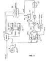
- Figure 3 represents in greater detail an example of a frequency conversion device.
- the video information input to the device is stored in the memory 8.
- This memory has a capacity of 4 fields and by virtue of dual read access, makes it possible to access 2 complete consecutive fields so as to carry out the interpolation. This makes it possible to avoid the problems of synchronization, the field read from a memory then being the last field stored in full in this memory. This is one example and the memory capacity can of course be lower, for example 3 fields, or less if one begins reading a field before it has been stored in full, this then requiring precautions with regard to the management of the pointers.
- the interpolation is carried out between the field T1 and the field immediately following it T2.
- a vertical synchronization signal V SYNC_IN hereinafter referred to as S1 is available at each input field.
- One pulse out of every four pulses is transmitted to the reset input (reset) of a write address counter 9, this being the signal V SYNC_IN/4 .
- the output of this counter is linked to the address inputs of the memory 8. It is also transmitted to the inputs of a register REG.IN 10 and of a register REG.OUT 11.
- the register REG.IN stores the value of the write pointer, that is to say the address P W_IN present on the address bus, on receipt of the input vertical synchronization signal V SYNC_IN transmitted on the clock input of the register.
- the register REG.OUT stores the value of the write pointer, that is to say the address P W_OUT present on the address bus, on receipt of the output vertical synchronization signal V SYNC_OUT transmitted on the clock input of the register.
- This signal V SYNC_OUT is also referred to as S2.
- a subtractor 12 receives the data P W_IN and P W_OUT provided by the registers 10 and 11. Its output (P W_OUT -P W_IN ) is signed and transmitted, as signal SGN, to a control input of a multiplexer 13 as well as to an input of a multiplier 14.
- the multiplexer 13 receives a zero input and an input equal to the constant N CAP expressing, as number of fields, the capacity of the memory 8. This multiplexer is driven by the signal SGN, in such a way that its output is set to the value 0 if (P W_OUT - P W_IN ) ⁇ 0 and to the value N CAP if (P W_OUT - P W_IN ) ⁇ 0.
- the second input of the adder originates from the output of the multiplexer 13.
- This signal is transmitted, after passing through a delay circuit 17, to the interpolator 20.
- the information P W_OUT originating from the register REG.OUT 11 is also transmitted to a storage and calculating circuit 16.
- This circuit stores the last value of the pointer P W_OUT . It provides, on its two outputs, a first loading value "loading 1" and a second loading value "loading 2". These loading values are modified for each output field. They are one field out of phase.
- the write pointer P W of the memory 8 is recorded upon receipt of a vertical synchronization pulse of the input signal (V SYNC_IN ) and upon receipt of a vertical synchronization pulse of the output signal (V SYNC_OUT ).
- the corresponding information P W_IN and P W_OUT respectively represent the start address of the current field recorded in the memory and the value of the pointer P W at the instant at which the synchronization pulse of the output signal is received, triggering the calculation of the new interpolated output field.
- t prev and t next be the instants of receipt of the previous and next reference field which are used for the calculation of the interpolated field, that is to say the instants of receipt of the synchronization signals of these fields.
- t interp be the temporal position of the interpolated field.
- N CAP. ⁇ P W_FIELD of the memory 8 is finite and the input fields are written thereto cyclically.
- N CAP 4 fields
- the writing of the fifth field will commence at the address 0 and will therefore overwrite the content of the first field.
- P W_OUT becomes less than P W_IN
- the correction to be made, if necessary, is carried out by the adder 15.
- the constant K transmitted as input to the multiplier 14 is the value 1 / ⁇ P W_FIELD
- the output from the adder 15 corresponds to the value ⁇ calculated at each arrival of the field synchronization signals.
- This coefficient ⁇ is delayed by the delay circuit 17 in such a way as to be able to be applied correctly to the set of fields T1 and T2.
- the storage and calculating circuit 16 calculates the read addresses relating to the two accesses of the memory 8.
- the value P W_OUT of the write pointer is stored. This value is used to calculate the start address for the reading of the fields T1 and T2 utilized for the interpolation. Given that four successive fields are stored in a memory, it is necessary to ascertain which one will be read and this depends on the position of the write pointer at the instant of receipt of the synchronization signal V SYNC_OUT .
- N is the number of addresses corresponding to a field and if the value of the pointer, upon receipt of the signal S2, lies between 0 and N, the loading value for the first field T1 to be read will be the address 2N and the loading value for the second field T2 to be read will be the address 3N, values corresponding to the last two complete fields loaded into the memory. If this value of the pointer lies between N and 2N, this signifies that the second field is being stored in the memory 8 and the loading value for the field T2 will then be the address 0.
- N is the number of addresses corresponding to a field and if the value of the pointer, upon receipt of the signal S2, lies between 0 and N, the loading value for the first field T1 to be read will be the address 2N and the loading value for the second field T2 to be read will be the address 3N, values corresponding to the last two complete fields loaded into the memory. If this value of the pointer lies between N and 2N, this signifies that the second field is being stored in the memory 8 and the loading value for
- Two read counters 18 and 19 receive, on a loading input, respectively the outputs "loading 1" and “loading 2" originating from the storage and calculating circuit 16.
- the loading validation inputs of the counters are supplied with the synchronization signal V SYNC_OUT .
- the values "loading 1" and “loading 2” are stored on receipt of the synchronization signal V SYNC_OUT .
- the counters are initialized to these values and their outputs are linked to the memory 8 to trigger the reading of the video data of the fields T1 and T2 from the memory on the basis of the initialization values.
- the video data read are transmitted to an interpolator 20 which carries out the calculation of the interpolated field, as a function of its temporal location defined by the value of ⁇ , in relation to the reference source fields T1 and T2, according to a known process, for example using spatio-temporal linear filtering or motion-compensated interpolation.
- the video data thus calculated are transmitted as output from the interpolator so as to constitute the output signal of the device.
- the previous calculations assume a continuous stream of data of the input video signal.
- the signals include a field blanking interval (VBI standing for Vertical Blanking Interval) during which the field flyback occurs.
- VBI standing for Vertical Blanking Interval
- ⁇ P W_VBI_start and ⁇ P W_VBI_end be the offsets or shifts corresponding to the write pointer in the video memory.
- ⁇ P W_VBI_start b ⁇ t VBI_start
- ⁇ P W_VBI_end b ⁇ t VBI_end
- the invention applies equally to frames if, for example, the input signal corresponds to a progressive type scanning. It is the successive frames which are then stored.
- the output signal which depends on the type of interpolation, can be of interlaced or progressive type without thereby departing from the domain of the invention.
Landscapes
- Engineering & Computer Science (AREA)
- Physics & Mathematics (AREA)
- Computer Hardware Design (AREA)
- General Physics & Mathematics (AREA)
- Theoretical Computer Science (AREA)
- Multimedia (AREA)
- Signal Processing (AREA)
- Television Systems (AREA)
Abstract
and in that it performs a phase interpolation (20) corresponding to this value.
Description
- The invention relates to a process and device for the frequency conversion of video signals, utilizing a dynamic calculation of the interpolation phases.
- Known frequency conversion devices are utilized, among other things, for standards conversion, for example the conversion of a PAL or SECAM 50Hz signal into an NTSC 60Hz signal. They are also utilized to increase the scanning frequency of television receivers, typically from 50 Hz to 100 Hz, for the purpose of improving the quality of the picture, by reducing the large area flicker.
- In the general case, the frequency of the signal to be converted and the frequency of the converted signal are known in advance. The interpolation process consists in creating intermediate fields between two reference fields of the input signal to be converted. This process is shown diagrammatically in Figure 1.
- The fields referenced 1 and 2 correspond respectively to the previous reference field of the input video sequence and to the next reference field of this sequence.
- The field referenced 3 is the intermediate field to be created. This field is located temporally between the previous field and the next field, at an instant defined by a value α corresponding to the interpolation phase.
- If tprev and tnext correspond to the instants relating to the previous field and to the next field, the instant tinterp relating to the intermediate field to be interpolated is then:
- In a known manner, the interpolation processing can call upon linear filtering utilizing spatio-temporal filters with finite impulse response, or upon motion-compensated interpolation.
- The processing methods utilized require knowledge of the interpolation phase for each field to be interpolated.
- In the case where the input or output signal is not bound to a standard defining its frequency, a conversion device specific to these signals and in particular to their scanning frequency characteristic must be designed. This specificity naturally generates high costs. Moreover, modification of the scanning characteristics of a signal renders such a device unutilizable or, at the least, requires either manual intervention to render it compatible with the modified signal or signals, or the presence of circuits specific to these new characteristics.
- The aim of the invention is to alleviate the aforesaid drawbacks.
- To this end, the invention relates to a process for the field or frame frequency conversion utilizing a dynamic calculation of the interpolation phases, of an input video signal at a frequency F1 defined by a synchronization signal S1 into an output video signal at a variable frequency F2 defined by a synchronization signal S2, comprising a writing of the input signal to a memory on the basis of a write pointer PW-IN, and a reading, from the memory, to obtain the output signal, characterized in that it stores the position of the write pointer PW on receipt of the synchronization signal S1 so as to provide a value PW-IN, and on receipt of the synchronization signal S2 so as to provide a value PW_OUT, in that it dynamically calculates an interpolation phase α such that:
and in that it performs a phase interpolation corresponding to this value. - According to a particular characteristic, three or four successive fields or frames are simultaneously stored in a memory and the interpolation is performed on the fields or frames preceding that being stored upon receipt of the signal S2 utilized for the calculation of the interpolation phase, on the basis of this calculated interpolation phase.
- According to another characteristic, the calculation of the interpolation phase takes into account a shift of the write pointer corresponding to the duration of the field or frame blanking signal before the active video.
- The invention also relates to a dynamic frequency conversion device for converting an input signal at a frequency F1 defined by a synchronization signal S1 into an output signal at a variable frequency F2 defined by the receipt of a synchronization signal S2, comprising a memory for writing the input signal on the basis of a write pointer PW, an interpolation circuit receiving the outputs from the memory for read-access to a preceding field or frame T1 and read-access to a next field or frame T2, characterized in that it also comprises:
- a circuit for storing the pointer PW on receipt of the signal S1 so as to provide a value PW_IN,
- a circuit for storing the pointer PW on receipt of the signal S2 so as to provide a value PW_OUT,
- a circuit for calculating interpolation phase
and in that the interpolation circuit is coupled to the calculating circuit so as to receive this interpolation phase and calculate the interpolated field or frame as a function of the interpolation phase. -
- By virtue of the invention, the process automatically calculates the interpolation phase corresponding to the output signal to be generated, when the scanning frequency of this output signal is not known a priori.
- The device obtained is compatible with any type of output signal, at least in a wide frequency range. The device is simple to implement and cheap. It makes it possible to supply adjustable scanning frequency apparatuses, such as monitors of PC-type personal computers.
- The characteristics and advantages of the present invention will be more apparent from the following description given by way of example and with reference to the appended figures in which:
- Figure 1 represents a field interpolation
- Figure 2 represents diagrammatically a frequency conversion device
- Figure 3 represents in detail a frequency conversion device
- Figure 4 represents field blanking intervals
- The device for field frequency conversion, implementing the process, is represented diagrammatically in Figure 2.
- An input video signal Video In is transmitted to a
memory interface circuit 4. Together with this signal is transmitted a horizontal and vertical synchronization signal H/VSYNC IN; a pulse indicates the start of a new line (horizontal synchronization) or of a new field (vertical synchronization). - The video information transported by the video signal relates to each pixel, a video line consisting of a succession of pixels and a field of a succession of lines. A RAM
dynamic video memory 5 stores at successive addresses the digital data travelling through thememory interface 4. The memory capacity is such that at least two consecutive fields can be stored. These two fields are the reference fields previously referred to as the previous field and the next field. - The output video signal Video Out is synchronous with the synchronization signal VSYNC_OUT originating from the apparatus supplied by the conversion device and corresponding to the desired scanning frequency. The video data stored in the
RAM 5 are transmitted, via a memory interface 6, to aninterpolation circuit 7. - This
interpolation circuit 7 therefore receives the signal VSYNC_OUT on the basis of which it calculates the interpolated frames. Given that the ratio of the frequencies of the input signal and of the output signal is not known a priori, the interpolation phases are calculated dynamically. The interpolation circuit therefore operates in an asynchronous manner with respect to the input signal and is controlled by the synchronization signal VSYNC_OUT originating from the apparatus supplied with the output video signal, for example originating from a graphics card of a PC-type computer monitor in the case of a TV→PC converter. - Figure 3 represents in greater detail an example of a frequency conversion device.
- The video information input to the device is stored in the
memory 8. This memory has a capacity of 4 fields and by virtue of dual read access, makes it possible to access 2 complete consecutive fields so as to carry out the interpolation. This makes it possible to avoid the problems of synchronization, the field read from a memory then being the last field stored in full in this memory. This is one example and the memory capacity can of course be lower, for example 3 fields, or less if one begins reading a field before it has been stored in full, this then requiring precautions with regard to the management of the pointers. - The interpolation is carried out between the field T1 and the field immediately following it T2.
- A vertical synchronization signal VSYNC_IN hereinafter referred to as S1, is available at each input field. One pulse out of every four pulses is transmitted to the reset input (reset) of a write address counter 9, this being the signal VSYNC_IN/4. The output of this counter is linked to the address inputs of the
memory 8. It is also transmitted to the inputs of a register REG.IN 10 and of a register REG.OUT 11. - The register REG.IN stores the value of the write pointer, that is to say the address PW_IN present on the address bus, on receipt of the input vertical synchronization signal VSYNC_IN transmitted on the clock input of the register.
- The register REG.OUT stores the value of the write pointer, that is to say the address PW_OUT present on the address bus, on receipt of the output vertical synchronization signal VSYNC_OUT transmitted on the clock input of the register. This signal VSYNC_OUT is also referred to as S2.
- A
subtractor 12 receives the data PW_IN and PW_OUT provided by theregisters multiplexer 13 as well as to an input of amultiplier 14. Themultiplexer 13 receives a zero input and an input equal to the constant NCAP expressing, as number of fields, the capacity of thememory 8. This multiplexer is driven by the signal SGN, in such a way that its output is set to thevalue 0 if (PW_OUT - PW_IN) ≥ 0 and to the value NCAP if (PW_OUT - PW_IN) < 0. The output of themultiplier 14, which on another input receives a value K equal to 1/ΔPW_FIELD, is transmitted to the input of anadder 15. The second input of the adder originates from the output of themultiplexer 13. The value of the output signal from theadder 15, which corresponds to the expression K(PW_OUT-PW_IN) or else K(PW_OUT - PW_IN) + NCAP depending on the sign of the signal SGN, represents the value of α. This signal is transmitted, after passing through adelay circuit 17, to theinterpolator 20. - The information PW_OUT originating from the
register REG.OUT 11 is also transmitted to a storage and calculatingcircuit 16. This circuit stores the last value of the pointer PW_OUT. It provides, on its two outputs, a first loading value "loading 1" and a second loading value "loading 2". These loading values are modified for each output field. They are one field out of phase. - The write pointer PW of the
memory 8 is recorded upon receipt of a vertical synchronization pulse of the input signal (VSYNC_IN) and upon receipt of a vertical synchronization pulse of the output signal (VSYNC_OUT). The corresponding information PW_IN and PW_OUT respectively represent the start address of the current field recorded in the memory and the value of the pointer PW at the instant at which the synchronization pulse of the output signal is received, triggering the calculation of the new interpolated output field. - Let tprev and tnext be the instants of receipt of the previous and next reference field which are used for the calculation of the interpolated field, that is to say the instants of receipt of the synchronization signals of these fields. Let tinterp be the temporal position of the interpolated field.
- According to Fig 1, we have:
- If b is the bit rate of entry to the
memory 8 of the words corresponding to the input video signal, in general the luminance signal, and if ΔPW_FIELD is the memory quantity required for the storage of an input field, we have, by the definition of PW_OUT and PW_IN: - In practice, the capacity NCAP.Δ PW_FIELD of the
memory 8 is finite and the input fields are written thereto cyclically. Thus, if their capacity is NCAP = 4 fields, after filling these memories starting from theaddress 0 with the first four fields received, the writing of the fifth field will commence at theaddress 0 and will therefore overwrite the content of the first field. In this configuration where PW_OUT becomes less than PW_IN, the previous formula for calculating α should be modified as follows: - PW-OUT - PW-IN is calculated by the
subtractor 12. - The correction to be made, if necessary, is carried out by the
adder 15. - The constant K transmitted as input to the
multiplier 14 is thevalue 1 / ΔPW_FIELD - This value is known a priori.
- The output from the
adder 15 corresponds to the value α calculated at each arrival of the field synchronization signals. This coefficient α is delayed by thedelay circuit 17 in such a way as to be able to be applied correctly to the set of fields T1 and T2. - The storage and calculating
circuit 16 calculates the read addresses relating to the two accesses of thememory 8. On receipt of the synchronization signal VSYNC_OUT, the value PW_OUT of the write pointer is stored. This value is used to calculate the start address for the reading of the fields T1 and T2 utilized for the interpolation. Given that four successive fields are stored in a memory, it is necessary to ascertain which one will be read and this depends on the position of the write pointer at the instant of receipt of the synchronization signal VSYNC_OUT. - If N is the number of addresses corresponding to a field and if the value of the pointer, upon receipt of the signal S2, lies between 0 and N, the loading value for the first field T1 to be read will be the address 2N and the loading value for the second field T2 to be read will be the address 3N, values corresponding to the last two complete fields loaded into the memory. If this value of the pointer lies between N and 2N, this signifies that the second field is being stored in the
memory 8 and the loading value for the field T2 will then be theaddress 0. We therefore have:
- The field T2 then corresponds to the value of "loading 2":

- Two read
counters circuit 16. The loading validation inputs of the counters are supplied with the synchronization signal VSYNC_OUT. The values "loading 1" and "loading 2" are stored on receipt of the synchronization signal VSYNC_OUT. The counters are initialized to these values and their outputs are linked to thememory 8 to trigger the reading of the video data of the fields T1 and T2 from the memory on the basis of the initialization values. - The video data read are transmitted to an
interpolator 20 which carries out the calculation of the interpolated field, as a function of its temporal location defined by the value of α, in relation to the reference source fields T1 and T2, according to a known process, for example using spatio-temporal linear filtering or motion-compensated interpolation. - The video data thus calculated are transmitted as output from the interpolator so as to constitute the output signal of the device.
- The previous calculations assume a continuous stream of data of the input video signal. In fact, the signals include a field blanking interval (VBI standing for Vertical Blanking Interval) during which the field flyback occurs.
- Two solutions can then be implemented:
- either the video signal, corresponding to this time span VBI, is written to the video memory, so causing occupation of memory by unutilized signals. The value PW_OUT - PW_IN then actually represents the time elapsed since the start of reception of the current field.
- or only the active part of the video signal is stored and it is then necessary to take into account the offset or shift generated by this signal VBI, in the manner described hereinbelow, with the aid of Figure 4. A time axis is symbolized in this Figure 4. VSYNC corresponds to the vertical synchronization signals. The video signal consists of a field blanking signal VBI (standing for Vertical Blanking Interval) preceding the active video, for a time ▵tVBI_start and of a VBI signal following the active video ▵tVBI_end.
- Let ▵PW_VBI_start and ▵PW_VBI_end be the offsets or shifts corresponding to the write pointer in the video memory.
- The value of α then becomes:
- If the request for a new output field arrives during the VBI interval, PW not being updated during these intervals, it is then possible to round the value of α to 0 or to 1 depending on whether this request arrives during the VBI interval preceding or following the active video.
- Concerning the line blanking signals (or horizontal blanking signals) corresponding to the line flyback, their duration is short enough to be neglected.
- The above reasoning were conducted with regard to signals with interlaced type scanning, that is to say with regard to fields. Of course, the invention applies equally to frames if, for example, the input signal corresponds to a progressive type scanning. It is the successive frames which are then stored. Likewise, the output signal, which depends on the type of interpolation, can be of interlaced or progressive type without thereby departing from the domain of the invention.
Claims (5)
- Process for the frequency conversion utilizing a dynamic calculation of the interpolation phases, of an input video signal at a frequency F1 defined by a synchronization signal S1 into an output video signal at a variable frequency F2 defined by a synchronization signal S2, comprising a writing of the input signal to a memory (8) on the basis of a write pointer PW and a reading, from the memory, to obtain the output signal, characterized in that it stores the position of the write pointer PW on receipt of the synchronization signal S1 so as to provide a value Pw-IN, and on receipt of the synchronization signal S2 so as to provide a value PW-OUT, in that it dynamically calculates an interpolation phase α (12, 13, 14, 15) such that:
and in that it performs a phase interpolation (20) corresponding to this value. - Process according to Claim 1, characterized in that three or four successive fields or frames are stored in the memory (8) and in that the interpolation is performed on the fields or frames following that being stored upon receipt of the signal S2 utilized for the calculation of the interpolation phase, on the basis of this calculated interpolation phase.
- Process according to Claim 1, characterized in that the calculation of the interpolation phase takes into account a shift of the write pointer corresponding to the duration of the field or frame blanking signal before the active video.
- Dynamic frequency conversion device for converting an input signal at a frequency F1 defined by a synchronization signal S1 into an output signal at a variable frequency F2 defined by the receipt of a synchronization signal S2, comprising a video memory (8) for writing the input signal on the basis of a write pointer PW, an interpolation circuit (20) receiving the outputs from the memory (8) for the reading of a field or frame T1 as first access followed by a next field or frame T2 as second access, characterized in that it also comprises:a circuit (10) for storing the pointer PW on receipt of the signal S1 so as to provide a value PW_IN,a circuit (11) for storing the pointer PW on receipt of the signal S2 so as to provide a value PW_OUT,a circuit (12, 13, 14, 15) for calculating interpolation phase
and in that the interpolation circuit (20) is coupled to the calculating circuit (12, 13, 14, 15) so as to receive this interpolation phase and calculate the interpolated field or frame as a function of the interpolation phase. - Device according to Claim 4, characterized in that the calculating circuit consists of a subtractor (12), a multiplexer (13), a multiplier (14) and an adder (15).
Applications Claiming Priority (2)
| Application Number | Priority Date | Filing Date | Title |
|---|---|---|---|
| FR9916053 | 1999-12-20 | ||
| FR9916053A FR2802754B1 (en) | 1999-12-20 | 1999-12-20 | METHOD AND DEVICE FOR FRAME OR IMAGE FREQUENCY CONVERSION USING A DYNAMIC CALCULATION OF INTERPOLATION PHASES |
Publications (2)
| Publication Number | Publication Date |
|---|---|
| EP1111917A1 true EP1111917A1 (en) | 2001-06-27 |
| EP1111917B1 EP1111917B1 (en) | 2007-04-25 |
Family
ID=9553467
Family Applications (1)
| Application Number | Title | Priority Date | Filing Date |
|---|---|---|---|
| EP00460071A Expired - Lifetime EP1111917B1 (en) | 1999-12-20 | 2000-12-14 | Method for dynamic computation of interpolation phases in a video standard converter |
Country Status (7)
| Country | Link |
|---|---|
| US (1) | US6630962B2 (en) |
| EP (1) | EP1111917B1 (en) |
| JP (1) | JP4733829B2 (en) |
| CN (1) | CN1163070C (en) |
| DE (1) | DE60034539T2 (en) |
| ES (1) | ES2284466T3 (en) |
| FR (1) | FR2802754B1 (en) |
Families Citing this family (2)
| Publication number | Priority date | Publication date | Assignee | Title |
|---|---|---|---|---|
| US8634023B2 (en) * | 2009-07-21 | 2014-01-21 | Qualcomm Incorporated | System for video frame synchronization using sub-frame memories |
| CN110248132B (en) * | 2019-05-31 | 2020-12-01 | 成都东方盛行电子有限责任公司 | Video frame rate interpolation method |
Citations (1)
| Publication number | Priority date | Publication date | Assignee | Title |
|---|---|---|---|---|
| EP0323198A2 (en) * | 1987-12-25 | 1989-07-05 | Nec Corporation | Television signal frame number converter |
Family Cites Families (5)
| Publication number | Priority date | Publication date | Assignee | Title |
|---|---|---|---|---|
| US6331862B1 (en) * | 1988-07-06 | 2001-12-18 | Lg Philips Lcd Co., Ltd. | Image expansion display and driver |
| JP3003826B2 (en) * | 1992-12-11 | 2000-01-31 | 三菱電機株式会社 | Clock recovery circuit |
| GB9401897D0 (en) * | 1994-02-01 | 1994-03-30 | Snell & Wilcox Ltd | Video processing |
| US6288745B1 (en) * | 1997-04-24 | 2001-09-11 | Mitsubishi Denki Kabushiki Kaisha | Scanner line interpolation device |
| US6407775B1 (en) * | 1999-04-16 | 2002-06-18 | Avid Technology, Inc. | Image resizer and frame rate converter with pulldown controller |
-
1999
- 1999-12-20 FR FR9916053A patent/FR2802754B1/en not_active Expired - Fee Related
-
2000
- 2000-12-14 DE DE60034539T patent/DE60034539T2/en not_active Expired - Lifetime
- 2000-12-14 EP EP00460071A patent/EP1111917B1/en not_active Expired - Lifetime
- 2000-12-14 ES ES00460071T patent/ES2284466T3/en not_active Expired - Lifetime
- 2000-12-18 JP JP2000383583A patent/JP4733829B2/en not_active Expired - Fee Related
- 2000-12-18 US US09/739,148 patent/US6630962B2/en not_active Expired - Lifetime
- 2000-12-20 CN CNB001206648A patent/CN1163070C/en not_active Expired - Fee Related
Patent Citations (1)
| Publication number | Priority date | Publication date | Assignee | Title |
|---|---|---|---|---|
| EP0323198A2 (en) * | 1987-12-25 | 1989-07-05 | Nec Corporation | Television signal frame number converter |
Also Published As
| Publication number | Publication date |
|---|---|
| JP4733829B2 (en) | 2011-07-27 |
| EP1111917B1 (en) | 2007-04-25 |
| JP2001211430A (en) | 2001-08-03 |
| US20010038421A1 (en) | 2001-11-08 |
| US6630962B2 (en) | 2003-10-07 |
| DE60034539D1 (en) | 2007-06-06 |
| CN1163070C (en) | 2004-08-18 |
| ES2284466T3 (en) | 2007-11-16 |
| FR2802754B1 (en) | 2002-03-15 |
| FR2802754A1 (en) | 2001-06-22 |
| CN1310550A (en) | 2001-08-29 |
| DE60034539T2 (en) | 2008-01-03 |
Similar Documents
| Publication | Publication Date | Title |
|---|---|---|
| KR100996216B1 (en) | High quality deinterlacing and frame multiplication circuits and methods | |
| EP0794525B1 (en) | Pixel conversion apparatus | |
| US6320619B1 (en) | Flicker filter circuit | |
| JP3257728B2 (en) | High quality TV picture-in-picture signal processing method and apparatus | |
| JP2736641B2 (en) | A device that freezes television images | |
| US5469228A (en) | Memory address and display control apparatus for high definition television | |
| US6160590A (en) | Video signal processing circuit inhibiting display of distorted images | |
| EP1111917B1 (en) | Method for dynamic computation of interpolation phases in a video standard converter | |
| US5777687A (en) | Image display system and multi-window image display method | |
| US5367343A (en) | Motion enhanced compressed video system | |
| EP0585903B1 (en) | Video signal memory equipment | |
| EP0582305B1 (en) | Video signal converting device and noise eliminator | |
| US6407778B1 (en) | Video signal processing | |
| EP1762092A1 (en) | Image processor and image processing method using scan rate conversion | |
| JP2779007B2 (en) | Noise reduction circuit | |
| JP2846427B2 (en) | PAL signal / CIF signal conversion circuit | |
| JP3545577B2 (en) | Scanning line converter | |
| JPH0918740A (en) | Frame synchronization method and frame synchronizer | |
| KR100348444B1 (en) | Television standard signal converter | |
| JP2584169B2 (en) | Television signal processor | |
| JP3018384B2 (en) | Video signal processing circuit | |
| JP3428180B2 (en) | Video signal compression device | |
| WO2001028242A1 (en) | Method and system for eliminating edge effects at the beginning of lines in video signals | |
| JPH02186878A (en) | Noise reduction device for television video signal | |
| Jaspers et al. | Synchronization of video in distributed computing systems |
Legal Events
| Date | Code | Title | Description |
|---|---|---|---|
| PUAI | Public reference made under article 153(3) epc to a published international application that has entered the european phase |
Free format text: ORIGINAL CODE: 0009012 |
|
| AK | Designated contracting states |
Kind code of ref document: A1 Designated state(s): DE ES FR GB IT |
|
| AX | Request for extension of the european patent |
Free format text: AL;LT;LV;MK;RO;SI |
|
| 17P | Request for examination filed |
Effective date: 20011217 |
|
| AKX | Designation fees paid |
Free format text: DE ES FR GB IT |
|
| GRAP | Despatch of communication of intention to grant a patent |
Free format text: ORIGINAL CODE: EPIDOSNIGR1 |
|
| RIC1 | Information provided on ipc code assigned before grant |
Ipc: G09G 5/00 20060101ALI20061016BHEP Ipc: H04N 7/01 20060101AFI20061016BHEP |
|
| GRAS | Grant fee paid |
Free format text: ORIGINAL CODE: EPIDOSNIGR3 |
|
| GRAA | (expected) grant |
Free format text: ORIGINAL CODE: 0009210 |
|
| AK | Designated contracting states |
Kind code of ref document: B1 Designated state(s): DE ES FR GB IT |
|
| REG | Reference to a national code |
Ref country code: GB Ref legal event code: FG4D |
|
| REF | Corresponds to: |
Ref document number: 60034539 Country of ref document: DE Date of ref document: 20070606 Kind code of ref document: P |
|
| ET | Fr: translation filed | ||
| REG | Reference to a national code |
Ref country code: ES Ref legal event code: FG2A Ref document number: 2284466 Country of ref document: ES Kind code of ref document: T3 |
|
| PLBE | No opposition filed within time limit |
Free format text: ORIGINAL CODE: 0009261 |
|
| STAA | Information on the status of an ep patent application or granted ep patent |
Free format text: STATUS: NO OPPOSITION FILED WITHIN TIME LIMIT |
|
| 26N | No opposition filed |
Effective date: 20080128 |
|
| PGFP | Annual fee paid to national office [announced via postgrant information from national office to epo] |
Ref country code: GB Payment date: 20101231 Year of fee payment: 11 Ref country code: IT Payment date: 20101223 Year of fee payment: 11 |
|
| PGFP | Annual fee paid to national office [announced via postgrant information from national office to epo] |
Ref country code: DE Payment date: 20101216 Year of fee payment: 11 Ref country code: FR Payment date: 20110118 Year of fee payment: 11 |
|
| PGFP | Annual fee paid to national office [announced via postgrant information from national office to epo] |
Ref country code: ES Payment date: 20110120 Year of fee payment: 11 |
|
| GBPC | Gb: european patent ceased through non-payment of renewal fee |
Effective date: 20111214 |
|
| REG | Reference to a national code |
Ref country code: FR Ref legal event code: ST Effective date: 20120831 |
|
| REG | Reference to a national code |
Ref country code: DE Ref legal event code: R119 Ref document number: 60034539 Country of ref document: DE Effective date: 20120703 |
|
| PG25 | Lapsed in a contracting state [announced via postgrant information from national office to epo] |
Ref country code: GB Free format text: LAPSE BECAUSE OF NON-PAYMENT OF DUE FEES Effective date: 20111214 Ref country code: DE Free format text: LAPSE BECAUSE OF NON-PAYMENT OF DUE FEES Effective date: 20120703 |
|
| PG25 | Lapsed in a contracting state [announced via postgrant information from national office to epo] |
Ref country code: IT Free format text: LAPSE BECAUSE OF NON-PAYMENT OF DUE FEES Effective date: 20111214 |
|
| PG25 | Lapsed in a contracting state [announced via postgrant information from national office to epo] |
Ref country code: FR Free format text: LAPSE BECAUSE OF NON-PAYMENT OF DUE FEES Effective date: 20120102 |
|
| REG | Reference to a national code |
Ref country code: ES Ref legal event code: FD2A Effective date: 20130703 |
|
| PG25 | Lapsed in a contracting state [announced via postgrant information from national office to epo] |
Ref country code: ES Free format text: LAPSE BECAUSE OF NON-PAYMENT OF DUE FEES Effective date: 20111215 |