EP1111724A2 - Electric socket apparatus - Google Patents
Electric socket apparatus Download PDFInfo
- Publication number
- EP1111724A2 EP1111724A2 EP00311589A EP00311589A EP1111724A2 EP 1111724 A2 EP1111724 A2 EP 1111724A2 EP 00311589 A EP00311589 A EP 00311589A EP 00311589 A EP00311589 A EP 00311589A EP 1111724 A2 EP1111724 A2 EP 1111724A2
- Authority
- EP
- European Patent Office
- Prior art keywords
- base
- seating surface
- cover
- rotary latch
- socket
- Prior art date
- Legal status (The legal status is an assumption and is not a legal conclusion. Google has not performed a legal analysis and makes no representation as to the accuracy of the status listed.)
- Withdrawn
Links
Images








Classifications
-
- H—ELECTRICITY
- H01—ELECTRIC ELEMENTS
- H01R—ELECTRICALLY-CONDUCTIVE CONNECTIONS; STRUCTURAL ASSOCIATIONS OF A PLURALITY OF MUTUALLY-INSULATED ELECTRICAL CONNECTING ELEMENTS; COUPLING DEVICES; CURRENT COLLECTORS
- H01R12/00—Structural associations of a plurality of mutually-insulated electrical connecting elements, specially adapted for printed circuits, e.g. printed circuit boards [PCB], flat or ribbon cables, or like generally planar structures, e.g. terminal strips, terminal blocks; Coupling devices specially adapted for printed circuits, flat or ribbon cables, or like generally planar structures; Terminals specially adapted for contact with, or insertion into, printed circuits, flat or ribbon cables, or like generally planar structures
- H01R12/70—Coupling devices
- H01R12/82—Coupling devices connected with low or zero insertion force
- H01R12/85—Coupling devices connected with low or zero insertion force contact pressure producing means, contacts activated after insertion of printed circuits or like structures
- H01R12/88—Coupling devices connected with low or zero insertion force contact pressure producing means, contacts activated after insertion of printed circuits or like structures acting manually by rotating or pivoting connector housing parts
-
- H—ELECTRICITY
- H01—ELECTRIC ELEMENTS
- H01R—ELECTRICALLY-CONDUCTIVE CONNECTIONS; STRUCTURAL ASSOCIATIONS OF A PLURALITY OF MUTUALLY-INSULATED ELECTRICAL CONNECTING ELEMENTS; COUPLING DEVICES; CURRENT COLLECTORS
- H01R33/00—Coupling devices specially adapted for supporting apparatus and having one part acting as a holder providing support and electrical connection via a counterpart which is structurally associated with the apparatus, e.g. lamp holders; Separate parts thereof
- H01R33/74—Devices having four or more poles, e.g. holders for compact fluorescent lamps
- H01R33/76—Holders with sockets, clips, or analogous contacts adapted for axially-sliding engagement with parallely-arranged pins, blades, or analogous contacts on counterpart, e.g. electronic tube socket
Definitions
- This inventions relates generally to a socket suitable for removably receiving an electrical part such as an integrated circuit (IC) having a plurality of terminals of the LGA or BGA, etc., type and more particularly to a socket for use in a burn-in test of the IC.
- IC integrated circuit
- such sockets have a base member made of an insulating material and have a plurality of contact members that correspond to the terminals arranged on one surface of the IC.
- the contact members are arranged on the seating surface of the socket to correspond to each terminal of the IC to be brought in touch with the same when the IC has been placed on the seating surface.
- a cover is provided for holding the IC on the seating surface, with the IC being held on and removed from the seating surface by moving the cover up and down.
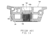
- one such prior art socket has one side of a cover 142 rotatably supported on a base 141.
- cover 142 When cover 142 is opened as shown in Fig. 14, IC 100 is placed onto seating surface 141a and cover 142 is closed by means of an automatic unit, not shown in the drawing.
- a hook 143 is engaged with a latch on base 141 to maintain cover 142 in a closed position.
- IC 100 on seating 141a is compressed from above by a compression surface 142a inside cover 142, with the terminals of the IC brought into engagement with the tip of respective contact members.
- a problem with this type of socket is that when closing cover 142, compression surface 142a approaches the base in a way which is inclined relative to IC 100 with a result that a bias load is applied to the IC.
- This biased load can damage the IC itself and, at the same time, can result in an uneven compressive force of the contact elements 144 against the terminals of the IC.
- the construction of the automatic unit for the switching action of cover 142 is complicated.
- Another type of prior art socket is equipped with a mechanism for the vertical movement of the cover member relative to the base member and a latch that opens or closes in linkage with the movement of the cover. It is generally the case that the latch opens when the cover member is lowered, thereby making it possible for the IC to be placed on the seating surface of the base and closes when the cover member is elevated, thereby making it possible for the IC on the seating surface to be held from above.
- This type of socket is subject to the following limitations:
- an object of the invention to provide a socket whose outside shape is comparatively small relative to the size of the IC that is to be tested. Another object of the invention is the provision of a socket which is easily and quickly assembled. Still another object of the invention is the provision of a socket having increased reliability of contact engagement of contact members with the terminals of the IC.
- the invention relates to a socket for use with an IC having a plurality of terminals on at least one surface thereof.
- a socket for use with a semiconductor device having a plurality of terminals on at least one surface comprising a base, a seating surface for a semiconductor device, a rotary latch having a rotational axis fixed to the base and having an opened position away from the seating surface to enable a semiconductor device to be placed on the seating surface and a closed position at the seating surface to enable a semiconductor device on the seating surface to be held from above, a cover which is arranged on the base and supported for movement between a first position which is close to the base and a second position which is separated from the base, and a link having one coupling mechanism connecting the link to the cover and another coupling mechanism connecting the link to the rotary latch which opens the rotary latch when the cover is at the first position and closes the rotary latch when the cover is at the second position, the coupling mechanism between the link and the rotary latch comprising a slot in the rotary latch which extends generally toward and away from the rotational axis of the rotary latch.
- the socket further comprises a spring for biasing the cover toward the second position.
- the rotational axis of the rotary latch is positioned below the seating surface.
- the seating surface is a surface of an adaptor member, which is received on the base, and has a plurality of contact member receiving holes extending through the seating surface and a plurality of contact members having tips received in each of the contact member receiving holes to be placed in contact with each terminal of the semiconductor device placed on the seating surface.
- the straight line distance between the coupling mechanism of the link to the cover and the rotational axis of the rotary latch varies in conformity with the position of the cover.
- the base may be formed with a guide surface for guiding the coupling mechanism of the link to the rotary latch to a position which is located closer to the rotational axis of the rotary latch when the rotary latch is opened and to a position which is separated from the rotational axis of the rotary latch when the rotary latch is closed.
- the base may have four sides and a rotary latch may be provided on at least two opposing sides of the base.
- the contact members have a convex configuration along their length with the tip parts being forced downwardly into the contact member receiving holes when a semiconductor device is placed on the seating surface, some of the plurality of contact members having the convex configuration facing in a first direction and other contact members having the convex configuration facing in second, different, direction. More preferably, approximately half of the plurality of contact members have their convex configuration facing in the first direction and approximately the remaining half have their convex configurations facing in the second, different, direction.
- the first direction and second, different, direction are opposite to each other.
- the plurality of contact members are arranged in a plurality of rows, with the convex configuration facing in the same direction in a given row.
- the socket may further comprise a mounting block fixed to the base, the adaptor member being movable toward and away from the mounting block and a spring member placing a bias on the adaptor member in a direction away from the mounting block.
- the mounting block holds the plurality of contact members.
- a socket has a seating surface for the IC on an adaptor received on a base with the adaptor being provided in such a way as to have a plurality of contact member receiving holes on the seating surface.
- the tips of a plurality of contact members corresponding to the terminals of the IC are, in that embodiment, received through the contact member receiving holes of the adaptor, thereby establishing contact with each terminal of the IC that has been placed on the seating surface.
- the IC on the seating surface is held by means of a rotary latch having a shaft fixed to the base and the latch has an open position for placement of the IC on the seating surface of the adaptor and a closed position for holding the IC on the seating surface from above the IC.
- the socket has a cover arranged over the base and a linking member that links the cover and the latch and the cover is supported for movement between a first position which is close to the base and a second position which is removed from the base.
- the linking member opens the latch when the cover is at the first position and closes the latch when the cover is at the second position.
- the rotary shaft of the latch is positioned below the seating surface of the adaptor.
- the cover preferably is normally biased away from the base to its second position.
- the straight line distance between the connecting point of the linking member and the latch and the rotary shaft of the latch varies in conformity with the position of the cover.
- the connecting point is guided by a slot formed in the latch which is elongated generally in the direction of the rotary shaft .
- a guide is provided on the base so that the connecting point will be guided to a position which is close to the rotary shaft of the latch when the latch is opened and to a position which is away from the rotary shaft of the latch when the latch is closed.
- the base preferably has four sides, with a latch being provided adjacent to two opposed sides. It is desirable for the adaptor to comprise an assembly having a fixed mounting block, a movable adaptor member and spring members.
- the mounting block may be fixed to the base for holding a plurality of contact members.
- the adaptor member has a seating surface for an IC device and is movably disposed on the mounting block, the adaptor member receiving the plurality of contact members within the seating surface and being supported in such a manner as to be in contact with or separated from the mounting block and the spring members bias the adaptor member in a direction away from the mounting block.
- the plurality of contact members each has a tip part that contacts a respective terminal of a semiconductor device placed on the seating surface and a curved part that provides a compressive force to the tip part against the terminal, some of the plurality of contact makers having the curved parts arranged to extend in a first direction and others having the curved parts arranged to extend in a second direction.
- approximately one half of the plurality of contact members have their curved parts arranged to extend in the first direction and approximately the remaining half have the curved part arranged to extend in the second direction.
- the first direction and the second direction are opposite to each other.
- the plurality of contact members are preferably arranged in a plurality of rows and their curved parts face in a single direction within a row.
- Socket 10 is made basically by incorporating an adaptor assembly 16 (see Fig. 2), including contact members 14, into a base assembly 12.
- Base assembly 12 comprises a base 18, shaped in a suitable configuration, such as rectangular when viewed from above, formed of an electrically insulating material such as plastic.
- Base 18 has a recessed part 18a for receiving adaptor assembly 16 in the center of the base.
- the lower part of contact members 14 protrude from the lower surface of the base through holes 18b when the adaptor assembly is inserted into recess 18a.
- Socket 10 is placed on a printed circuit substrate, not shown in the drawing, and each contact member 14 is electrically connected to the circuit pattern on the substrate.
- Base assembly 12 also includes a cover 20, shaped in correspondence with base 18, formed of an electrically insulating material such as plastic.
- Cover 20 is movably mounted on base 18 toward and away from the base in a perpendicular direction.
- the center of cover 20 is formed with an opening 20a to permit insertion of IC 100 from above the socket.
- Four springs 21 are arranged at the corners of the socket between base 18 and cover 20 to bias the cover away from the base as shown in Figs. 1B, 1C and 2. That is, the force of springs 21 cause cover 20 to normally assume a position which is raised relative to base 18.
- an outwardly extending stop surface 18d of base 18 and an inwardly extending stop surface 20b of the cover are engaged (see Fig. 3).
- Cover 20 is linked to base 18 through a pair of latches 22 and four links 24 that are included in base assembly 12.
- the function of latches 22 is to fix or hold an IC 100 that has been placed inside socket 10.
- the latches are rotatable between an opened position and a closed position in linkage with vertical movement of cover 20 by means of links 24. Details of the latches 22 and their operation will be described below.
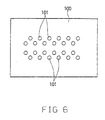
- Adaptor assembly 16 includes contact members 14, whose number and placement correspond to the number and placement of terminal pads 101 of an IC 100 that is to be tested (see Fig. 6), a mounting block 26 that holds contact members 14 and an adaptor member 28 that is placed thereon.
- Mounting block 26 is made of an electrically insulating material such as plastic and has slots 26a for receipt of respective contact members 14 running vertically through the slots.
- Each contact member 14 is engaged and held at the lower portion of a hole 18b at an engagement part 14a which is located approximately at the center of the contact member.
- slots 26a are formed having an expanded width to allow curved part 14b of the contact members to freely assume a curved configuration therein.
- An engagement latch 26b is formed on the outer peripheral wall of mounting block 26 which is engaged with engagement latch 18c of base 18 to fixedly attach mounting block 26 to base 18. Further, an inwardly extending engagement latch 26c is formed on the mounting block 26 and this engages with an outwardly extending engagement latch 28a of adaptor member 28.
- Adaptor member 28 is made of an electrically insulating material such as plastic and is arranged on mounting block 26. Adaptor member 28 is vertically movable relative to mounting block 26 having a comparatively small stroke. Four coil springs 30 are placed between the base and adaptor member 28 to bias the adaptor member upwardly relative to mounting block 26. When adaptor member 28 is raised, as shown in Fig. 5, engagement latch 26c of mounting block 26 and engagement latch 28a of adaptor 28 are engaged with each other thereby limiting the stroke of movement.
- Adaptor member 28 has a seating surface 28b for IC 100 on its upper surface. Seating surface 28b corresponds to the generally planar lower surface of IC 100, with its periphery being defined by the lower end of wall 28c.
- an IC 100 that has been placed on seating surface 28b has its approximate position determined by wall 28c.
- receiving holes 28d are located on seating surface 28b of adaptor 28 in conformity with the position of pads 101 of IC 100.
- Tip 14c of each respective contact member 14 mounted in mounting block 28 protrudes slightly from a receiving hole 28d and it contacts a pad 101 of an IC on seating surface 28b.
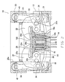
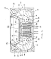
- Each latch 22 is formed of an electrically insulating material such as plastic and has a selected length that extends along one of the sides of IC 100 (see Figs. 1A, 3 and 5) and, at the same time, its front elevation has a shape similar to the claw of a crab (see Figs. 2 and 4).
- latches 22 are arranged to face each other along two opposing sides of IC 100 and are rotatably supported on base 18 by means of respective shafts 32.
- Each shaft 32 has both ends thereof installed in base 18 at a location lower than seating surface 28b of adaptor member 28.
- a recessed portion 22b is formed on each latch 22 to avoid interference with adaptor member 28 as well as IC 100 so IC 100 can be depressed from above by tip 22a as shown in Fig. 2 despite the position of the rotational fulcrum of shaft 32.
- Two pairs of links 24 extend generally vertically downwardly supported by shafts 40 on cover 20 with each pair connected at their bottom portions to opposite ends of a respective latch 22.
- An elongated slot 22c is provided in each latch 22 and a shaft 34 that is installed at the lower end portion of each link 24 is movably received through the slot. Slots 22c of latches 22 extend in such a direction that the respective shaft 34 can generally approach or move away from shaft 32 of the respective latch 22.
- shafts 34 are located at the outer extremity of slots 22c at a position which is furthest away from shafts 32 and links 24 are approximately in a vertical position.
- shafts 34 are located at the inner extremity of slots 22c, or a position which is close to the respective shafts 32 with the bottom portion of links 24 pulled inwardly so that the links are tilted from the perpendicular direction.
- a guide groove 36 is formed in base 18 for guiding the bottom of each link 24 and respective shaft 34, i.e., connecting point, when cover 20 is moved. When cover 20 is pressed downwardly from the Fig. 2 to the Fig.
- socket 10 is in the state shown in Figs. 2 and 3.
- cover 20 is in the raised position relative to base 18 by the force of springs 21 and latches 22 are closed.
- cover 20 is pressed downwardly toward base 18 by an automatic unit, not shown in the drawing, the bottom of links 24 start on their guided path toward the center of the base in conformity with guide grooves 36.
- latches 22 start their outwardly rotation.
- the IC 100 that is supplied onto adaptor member 28 through opening 20a of cover 20 is positioned and arranged on the seating surface 28b with each pad 101 of the IC 100 lightly engaging the tip 14c of a contact member 14 that extends through a respective receiving hole 28d of adaptor member 28.
- cover 20 rises due to the force of springs 21 pulling links 24 upwardly and their bottom portions shifting toward the outside of base 18 in conformity with guide groove 36.
- latches 22 are rotated about shafts 32 with their tips 22a extending toward the top of IC 100 and finally pressing down IC 100 from above as shown in Figs. 2 and 3. Because of the compressive force from latches 22, adaptor member 28 is pushed down against the force of springs 30 so that the curve of each contact member 14 at intermediate portions 14b is increased along with the contact force with the respective pads 101 of the IC.
- contact members 14 in the Figs. 5 and 3 positions are shown respectively in Figs. 7A and 7B.
- Each receiving hole 28d is enlarged along its width on the seating surface side at 70 and has an enlarged tapered opening 72 on the side opposite to seating surface 28b.
- tip 14c of each respective contact member 14 is held by a narrow supporting neck part 74 located between the enlarged openings 70 and 72. Due to the curve of each curved part 14b conforming to the vertical movement of adaptor 28, the orientation of each tip 14c shifts laterally, albeit slightly, using support part 74 as a fulcrum. In other words, the point of engagement of contact members 14 with pads 101 shift because of the enlarged opening at 70.
- tips 14c of contact members 14 move horizontally, while maintaining their engagement with the respective pads 101 of IC 100 as shown in Fig. 7B. As a result of this, tips 14c of the contact members wipe the surfaces of pads 101. Because of this wiping acting, the electrical reliability of the connection at the tips is enhanced.
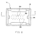
- a plan view of adaptor assembly 16 shows adaptor member 28 with seating surface 28b for IC 100, walls 28c around the seating surface and the receiving holes 28d for the contact members formed in the seating surface.
- the receiving holes 28d on the seating surface 28b are arranged in four rows in the longitudinal direction at locations in conformity with the pads 101 of IC 100 as shown in Fig. 6.
- Tip 14c of each contact member 14 is inserted in a respective receiving hole 28d, as described earlier, subsequent to the preparation of the adaptor assembly; however, the contact members are disposed so that the curved portions 14b extend in different directions in the two rows of receiving holes on the outside and the two rows of receiving holes on the inside.
- each contact member 14 is inserted in such a way as to form a convex configuration in a first or right-hand direction for the two rows of receiving holes 28d on the outside, while the curved part 14b is inserted in such a manner as to form a convex configuration in the opposite, second or left hand direction for the two rows of receiving holes 28d on the inside.
- Figs. 3 and 5 show the cross section taken along line 3-3 in Fig. 8 showing the adaptor assembly 16.
- the wiping at tips 14c of the contact members tend to move IC 100 in a given direction.
- Socket 10 is composed of base assembly 12 and adaptor assembly 16, with each assembly being built in parallel, followed by the incorporation of the adaptor assembly into the base assembly.
- Figs. 9A-9E show the procedures for assembling base assembly 12.
- Fig. 9A four links 24 are installed on cover 20 by using shafts 40.
- Fig. 9B latches 22 are arranged between a respective pair of links 24, and as shaft 34 is inserted into each respective pair, cover 20 is attached to the latches. In this manner, the cover assembly 38 is completed.
- cover assembly 38 is installed on base 18 through four springs 21.
- cover assembly 38 is attached in such a manner as to be capable of vertical movement relative to base 18.
- rotary shaft 32 is inserted from the side of base 18 and each latch 22 is rotatably installed on base 18. In this manner, the assembly is completed.
- Figs. 10A-10C show the order of the assembling of adaptor assembly 16.
- adaptor member 28 is installed on mounting block 26 through four springs 30.
- engaging latch 28a on the sides of the adaptor member engage with the engaging latch 26c (not shown in Fig. 10A) on the side of the mounting block, thereby making it possible for adaptor member 28 to be mounted on mounting block 26 in such a fashion as to be vertically movable relative to the mounting block.
- Fig. 10B the mounting block and adaptor member are inverted and contact members 14 are placed inside mounting block 26 by employing a pedestal 110.
- the adaptor assembly 16 is completed as seen in Fig. 10C.
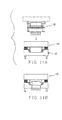
- Figs. 11A, 11 B show the final assembling steps for socket 10.
- the adaptor assembly 16 that has been assembled as shown in Fig. 10C is incorporated, from above, into base assembly 12 that has been assembled in the steps shown in Figs. 9A-9E above.
- the engagement latch 18c on the side of the base assembly and the engagement latch 26b on the side of the adaptor assembly are engaged with each other. (Reference should be made to Figs. 3 and 5.)
- socket 10 is finally assembled as indicated in Fig. 11B.
- the assembling of base assembly 12 in steps shown in Figs. 9A-9E
- the assembling of adaptor assembly 16 in steps shown in Figs. 10A-10C
- the assembling of base assembly 12 in steps shown in Figs. 9A-9E
- the assembling of adaptor assembly 16 in steps shown in Figs. 10A-10C
- FIG. 12 A drawing of socket 10 corresponding to Fig. 2 is shown in Fig. 12 showing adaptor assembly 16, cover assembly 38 and base 18 separated from one another. Cover assembly 38 is installed on base 18 in accordance with the steps described earlier and adaptor assembly 16 is then installed.
- the outside shape of the socket as compared with the size of the IC to be tested can be decreased.
- the socket is composed of a plurality of assemblies, with a result that the time required for assembling the socket can be shortened. Further, according to the invention, the wiping at the tip of the contact maker can be carried out effectively and, accordingly, the connective reliability for the IC terminals can be improved.
Landscapes
- Connecting Device With Holders (AREA)
- Testing Of Individual Semiconductor Devices (AREA)
- Connector Housings Or Holding Contact Members (AREA)
Abstract
Description
Claims (13)
- A socket for use with a semiconductor device having a plurality of terminals on at least one surface, comprising a base, a seating surface for a semiconductor device, a rotary latch having a rotational axis fixed to the base and having an opened position away from the seating surface to enable a semiconductor device to be placed on the seating surface and a closed position at the seating surface to enable a semiconductor device on the seating surface to be held from above, a cover which is arranged on the base and supported for movement between a first position which is close to the base and a second position which is separated from the base, and a link having one coupling mechanism connecting the link to the cover and another coupling mechanism connecting the link to the rotary latch which opens the rotary latch when the cover is at the first position and closes the rotary latch when the cover is at the second position, the coupling mechanism between the link and the rotary latch comprising a slot in the rotary latch which extends generally toward and away from the rotational axis of the rotary latch.
- A socket according to claim 1, wherein the seating surface is a surface of an adaptor member, which is received on the base, and has a plurality of contact member receiving holes extending through the seating surface and a plurality of contact members having tips received in each of the contact member receiving holes to be placed in contact with each terminal of the semiconductor device placed on the seating surface.
- A socket according to claim 1 or claim 2 further comprising a spring for biasing the cover toward the second position.
- A socket according to any of claims 1 to 3, wherein the rotational axis of the rotary latch is positioned below the seating surface.
- A socket according to claim 4, wherein the straight line distance between the coupling mechanism of the link to the cover and the rotational axis of the rotary latch varies in conformity with the position of the cover.
- A socket according to any preceding claim, wherein the base is formed with a guide surface for guiding the coupling mechanism of the link to the rotary latch to a position which is located closer to the rotational axis of the rotary latch when the rotary latch is opened and to a position which is separated from the rotational axis of the rotary latch when the rotary latch is closed.
- A socket according to any preceding claim, wherein the base has four sides and a rotary latch is provided on at least two opposing sides of the base.
- A socket according to any preceding claim, wherein the contact members have a convex configuration along their length with the tip parts being forced downwardly into the contact member receiving holes when a semiconductor device is placed on the seating surface, some of the plurality of contact members having the convex configuration facing in a first direction and other contact members having the convex configuration facing in second, different, direction.
- A socket as described in claim 8, in which approximately half of the plurality of contact members have their convex configuration facing in the first direction and approximately the remaining half have their convex configurations facing in the second, different, direction.
- A socket according to claim 8 or claim 9, in which the first direction and second, different, direction are opposite to each other.
- A socket according to any of claims 8 to 10, in which the plurality of contact members are arranged in a plurality of rows, with the convex configuration facing in the same direction in a given row.
- A socket according to any preceding claim, further comprising a mounting block fixed to the base, the adaptor member being movable toward and away from the mounting block and a spring member placing a bias on the adaptor member in a direction away from the mounting block.
- A socket according to claim 12, in which the mounting block holds the plurality of contact members.
Applications Claiming Priority (2)
| Application Number | Priority Date | Filing Date | Title |
|---|---|---|---|
| JP36657499 | 1999-12-24 | ||
| JP36657499A JP4301669B2 (en) | 1999-12-24 | 1999-12-24 | socket |
Publications (2)
| Publication Number | Publication Date |
|---|---|
| EP1111724A2 true EP1111724A2 (en) | 2001-06-27 |
| EP1111724A3 EP1111724A3 (en) | 2002-06-12 |
Family
ID=18487127
Family Applications (1)
| Application Number | Title | Priority Date | Filing Date |
|---|---|---|---|
| EP00311589A Withdrawn EP1111724A3 (en) | 1999-12-24 | 2000-12-21 | Electric socket apparatus |
Country Status (4)
| Country | Link |
|---|---|
| US (1) | US6322384B1 (en) |
| EP (1) | EP1111724A3 (en) |
| JP (1) | JP4301669B2 (en) |
| KR (1) | KR100654262B1 (en) |
Cited By (8)
| Publication number | Priority date | Publication date | Assignee | Title |
|---|---|---|---|---|
| US7118386B2 (en) | 2002-12-17 | 2006-10-10 | Yamaichi Electronics Co., Ltd. | Socket for semiconductor device |
| US7230830B2 (en) | 2004-04-16 | 2007-06-12 | Yamaichi Electronics Co., Ltd. | Semiconductor device socket |
| US7335030B2 (en) | 2005-03-10 | 2008-02-26 | Yamaichi Electronics Co., Ltd. | Cartridge for contact terminals and semiconductor device socket provided with the same |
| US7568918B2 (en) | 2007-09-28 | 2009-08-04 | Yamaichi Electronics Co., Ltd. | Socket for semiconductor device |
| US7618277B2 (en) | 2004-08-31 | 2009-11-17 | Yamaichi Electronics Co., Ltd. | Method of mounting and demounting a semiconductor device, device for mounting and demounting a semiconductor device using the same, and socket for a semiconductor device |
| US7887355B2 (en) | 2008-11-13 | 2011-02-15 | Yamaichi Electronics Co., Ltd. | Semiconductor device socket |
| EP1952491A4 (en) * | 2005-10-17 | 2012-01-04 | 3M Innovative Properties Co | Socket for electronic devices |
| WO2012159677A1 (en) * | 2011-05-26 | 2012-11-29 | Ismeca Semiconductor Holding Sa | Clamp |
Families Citing this family (25)
| Publication number | Priority date | Publication date | Assignee | Title |
|---|---|---|---|---|
| JP3789789B2 (en) * | 2001-08-31 | 2006-06-28 | 株式会社エンプラス | Socket for electrical parts |
| JP4721582B2 (en) * | 2001-09-14 | 2011-07-13 | 株式会社センサータ・テクノロジーズジャパン | socket |
| US6547580B1 (en) * | 2001-09-24 | 2003-04-15 | Texas Instruments Incorporated | Socket apparatus particularly adapted for land grid array type semiconductor devices |
| JP2003133022A (en) * | 2001-10-26 | 2003-05-09 | Yamaichi Electronics Co Ltd | IC socket |
| JP4439151B2 (en) * | 2001-10-31 | 2010-03-24 | 株式会社リコー | IC socket |
| JP2003168532A (en) | 2001-11-29 | 2003-06-13 | Texas Instr Japan Ltd | Semiconductor device socket and method of attaching semiconductor device to socket |
| JP3566691B2 (en) | 2001-12-17 | 2004-09-15 | 日本テキサス・インスツルメンツ株式会社 | Semiconductor device socket and method of attaching semiconductor device to socket |
| JP4022066B2 (en) * | 2001-12-28 | 2007-12-12 | 株式会社エンプラス | Member mounting structure |
| JP3942936B2 (en) * | 2002-04-09 | 2007-07-11 | 株式会社エンプラス | Socket for electrical parts |
| JP3531644B2 (en) * | 2002-05-31 | 2004-05-31 | 沖電気工業株式会社 | Semiconductor socket and probe replacement method for the socket |
| TW554586B (en) * | 2002-07-23 | 2003-09-21 | Nanya Technology Corp | Socket of chip scale package |
| KR100496634B1 (en) * | 2002-10-01 | 2005-06-20 | 미래산업 주식회사 | Test Socket |
| JP3737078B2 (en) * | 2002-10-29 | 2006-01-18 | 日本テキサス・インスツルメンツ株式会社 | Socket for semiconductor device and method for attaching / detaching semiconductor device to / from socket |
| JP2005327628A (en) * | 2004-05-14 | 2005-11-24 | Three M Innovative Properties Co | IC socket |
| KR100665065B1 (en) | 2005-05-13 | 2007-01-05 | 삼성전자주식회사 | Semiconductor device test device |
| TWI318480B (en) * | 2005-07-15 | 2009-12-11 | Hon Hai Prec Ind Co Ltd | Electrical connector |
| JP4786409B2 (en) * | 2006-05-18 | 2011-10-05 | 株式会社エンプラス | Socket for electrical parts |
| JP4786408B2 (en) * | 2006-05-18 | 2011-10-05 | 株式会社エンプラス | Socket for electrical parts |
| JP2009036679A (en) * | 2007-08-02 | 2009-02-19 | Yamaichi Electronics Co Ltd | Socket for semiconductor device |
| KR101053462B1 (en) * | 2008-08-26 | 2011-08-03 | 이종욱 | Semiconductor device test socket |
| JP5197297B2 (en) * | 2008-10-17 | 2013-05-15 | スリーエム イノベイティブ プロパティズ カンパニー | IC socket |
| CN201549659U (en) * | 2009-06-02 | 2010-08-11 | 富士康(昆山)电脑接插件有限公司 | Electric connector |
| KR101538427B1 (en) * | 2014-02-28 | 2015-07-24 | ㈜킴스옵텍 | LED Socket for Testing Spectrum Property |
| KR101689392B1 (en) * | 2015-06-19 | 2017-01-02 | (주)마이크로컨텍솔루션 | Test socket |
| KR102639116B1 (en) * | 2015-12-16 | 2024-02-20 | 엘지디스플레이 주식회사 | Apparatus for inspecting display apparatus |
Family Cites Families (5)
| Publication number | Priority date | Publication date | Assignee | Title |
|---|---|---|---|---|
| JP2665419B2 (en) * | 1991-08-13 | 1997-10-22 | 山一電機株式会社 | Connector for electrical components |
| JPH08162239A (en) * | 1994-12-02 | 1996-06-21 | Texas Instr Japan Ltd | socket |
| JP2667647B2 (en) * | 1994-12-29 | 1997-10-27 | 山一電機株式会社 | IC socket |
| JP2667646B2 (en) * | 1994-12-29 | 1997-10-27 | 山一電機株式会社 | IC socket |
| US5865639A (en) | 1996-06-25 | 1999-02-02 | Texas Instruments Incorporated | Burn-in test socket apparatus |
-
1999
- 1999-12-24 JP JP36657499A patent/JP4301669B2/en not_active Expired - Fee Related
-
2000
- 2000-11-03 US US09/706,379 patent/US6322384B1/en not_active Expired - Lifetime
- 2000-12-21 EP EP00311589A patent/EP1111724A3/en not_active Withdrawn
- 2000-12-22 KR KR1020000080185A patent/KR100654262B1/en not_active Expired - Fee Related
Cited By (13)
| Publication number | Priority date | Publication date | Assignee | Title |
|---|---|---|---|---|
| US7118386B2 (en) | 2002-12-17 | 2006-10-10 | Yamaichi Electronics Co., Ltd. | Socket for semiconductor device |
| US7165978B2 (en) | 2002-12-17 | 2007-01-23 | Yamichi Electronics Co., Ltd. | Socket for semiconductor device |
| US7204708B2 (en) | 2002-12-17 | 2007-04-17 | Yamaichi Electronics Co., Ltd. | Socket for semiconductor device |
| US7278868B2 (en) | 2002-12-17 | 2007-10-09 | Yamaichi Electronics Co., Ltd. | Socket for semiconductor device |
| US7230830B2 (en) | 2004-04-16 | 2007-06-12 | Yamaichi Electronics Co., Ltd. | Semiconductor device socket |
| US7618277B2 (en) | 2004-08-31 | 2009-11-17 | Yamaichi Electronics Co., Ltd. | Method of mounting and demounting a semiconductor device, device for mounting and demounting a semiconductor device using the same, and socket for a semiconductor device |
| US7556507B2 (en) | 2005-03-10 | 2009-07-07 | Yamaichi Electronics Co., Ltd. | Cartridge for contact terminals and semiconductor device socket provided with the same |
| US7563144B2 (en) | 2005-03-10 | 2009-07-21 | Yamaichi Electronics Co., Ltd. | Cartridge for contact terminals and semiconductor device socket provided with the same |
| US7335030B2 (en) | 2005-03-10 | 2008-02-26 | Yamaichi Electronics Co., Ltd. | Cartridge for contact terminals and semiconductor device socket provided with the same |
| EP1952491A4 (en) * | 2005-10-17 | 2012-01-04 | 3M Innovative Properties Co | Socket for electronic devices |
| US7568918B2 (en) | 2007-09-28 | 2009-08-04 | Yamaichi Electronics Co., Ltd. | Socket for semiconductor device |
| US7887355B2 (en) | 2008-11-13 | 2011-02-15 | Yamaichi Electronics Co., Ltd. | Semiconductor device socket |
| WO2012159677A1 (en) * | 2011-05-26 | 2012-11-29 | Ismeca Semiconductor Holding Sa | Clamp |
Also Published As
| Publication number | Publication date |
|---|---|
| KR20010062623A (en) | 2001-07-07 |
| EP1111724A3 (en) | 2002-06-12 |
| JP2001185313A (en) | 2001-07-06 |
| JP4301669B2 (en) | 2009-07-22 |
| US6322384B1 (en) | 2001-11-27 |
| KR100654262B1 (en) | 2006-12-07 |
Similar Documents
| Publication | Publication Date | Title |
|---|---|---|
| US6322384B1 (en) | Electrical socket apparatus | |
| US5518410A (en) | Contact pin device for IC sockets | |
| JP4251423B2 (en) | socket | |
| KR100642094B1 (en) | Socket for removably mounting electronic parts having a plurality of conductive terminals such as bga packages | |
| US6261114B1 (en) | Socket for electrical parts | |
| US20030114034A1 (en) | Socket for mounting an electronic device | |
| KR101245837B1 (en) | Socket device for testing a ic package | |
| US6899558B2 (en) | Socket for electrical parts | |
| KR20150002981A (en) | Socket device for testing an IC | |
| KR960009284A (en) | Socket device | |
| US6743034B2 (en) | Socket for electrical parts | |
| US6375484B1 (en) | Electrical part socket with pivotable latch | |
| US6383002B1 (en) | Heat sink for an electrical part assembly | |
| US6139348A (en) | Electric connector with an elastically deformable contact pin | |
| JP3789789B2 (en) | Socket for electrical parts | |
| KR20010013206A (en) | Burn-in test socket | |
| US20030076123A1 (en) | Socket apparatus and method for removably mounting an electronic package | |
| US20020151203A1 (en) | Open top IC socket | |
| KR100539350B1 (en) | Ic test socket | |
| KR20010015435A (en) | Socket for electrical parts | |
| US7134892B2 (en) | Socket for electrical parts | |
| US6428337B2 (en) | Socket for electrical parts | |
| US6857888B2 (en) | Socket for electrical parts | |
| US20030123241A1 (en) | Mount structure | |
| JP2004228042A (en) | Socket for electric component |
Legal Events
| Date | Code | Title | Description |
|---|---|---|---|
| PUAI | Public reference made under article 153(3) epc to a published international application that has entered the european phase |
Free format text: ORIGINAL CODE: 0009012 |
|
| AK | Designated contracting states |
Kind code of ref document: A2 Designated state(s): AT BE CH CY DE DK ES FI FR GB GR IE IT LI LU MC NL PT SE TR |
|
| AX | Request for extension of the european patent |
Free format text: AL;LT;LV;MK;RO;SI |
|
| PUAL | Search report despatched |
Free format text: ORIGINAL CODE: 0009013 |
|
| AK | Designated contracting states |
Kind code of ref document: A3 Designated state(s): AT BE CH CY DE DK ES FI FR GB GR IE IT LI LU MC NL PT SE TR |
|
| AX | Request for extension of the european patent |
Free format text: AL;LT;LV;MK;RO;SI |
|
| AKX | Designation fees paid | ||
| REG | Reference to a national code |
Ref country code: DE Ref legal event code: 8566 |
|
| STAA | Information on the status of an ep patent application or granted ep patent |
Free format text: STATUS: THE APPLICATION IS DEEMED TO BE WITHDRAWN |
|
| 18D | Application deemed to be withdrawn |
Effective date: 20021213 |