EP1111406A2 - Strahlungsnachweisgerät - Google Patents
Strahlungsnachweisgerät Download PDFInfo
- Publication number
- EP1111406A2 EP1111406A2 EP00969049A EP00969049A EP1111406A2 EP 1111406 A2 EP1111406 A2 EP 1111406A2 EP 00969049 A EP00969049 A EP 00969049A EP 00969049 A EP00969049 A EP 00969049A EP 1111406 A2 EP1111406 A2 EP 1111406A2
- Authority
- EP
- European Patent Office
- Prior art keywords
- transistor
- load
- radiation
- electrode
- pulse generator
- Prior art date
- Legal status (The legal status is an assumption and is not a legal conclusion. Google has not performed a legal analysis and makes no representation as to the accuracy of the status listed.)
- Granted
Links
- 230000005855 radiation Effects 0.000 title claims abstract description 80
- 239000003990 capacitor Substances 0.000 claims abstract description 32
- 230000035945 sensitivity Effects 0.000 abstract description 9
- 238000001514 detection method Methods 0.000 abstract description 5
- 230000004048 modification Effects 0.000 description 14
- 238000012986 modification Methods 0.000 description 14
- 230000005865 ionizing radiation Effects 0.000 description 5
- 230000003287 optical effect Effects 0.000 description 5
- 238000004980 dosimetry Methods 0.000 description 3
- 230000005669 field effect Effects 0.000 description 3
- 239000002245 particle Substances 0.000 description 3
- 238000005375 photometry Methods 0.000 description 3
- 230000009471 action Effects 0.000 description 2
- 238000000034 method Methods 0.000 description 2
- 241001313099 Pieris napi Species 0.000 description 1
- XUIMIQQOPSSXEZ-UHFFFAOYSA-N Silicon Chemical compound [Si] XUIMIQQOPSSXEZ-UHFFFAOYSA-N 0.000 description 1
- 230000003213 activating effect Effects 0.000 description 1
- 230000004913 activation Effects 0.000 description 1
- 238000004458 analytical method Methods 0.000 description 1
- 238000003491 array Methods 0.000 description 1
- 230000001143 conditioned effect Effects 0.000 description 1
- 238000010276 construction Methods 0.000 description 1
- 230000008878 coupling Effects 0.000 description 1
- 238000010168 coupling process Methods 0.000 description 1
- 238000005859 coupling reaction Methods 0.000 description 1
- 239000013078 crystal Substances 0.000 description 1
- 230000003247 decreasing effect Effects 0.000 description 1
- 238000002050 diffraction method Methods 0.000 description 1
- 239000003814 drug Substances 0.000 description 1
- 238000002474 experimental method Methods 0.000 description 1
- 230000004907 flux Effects 0.000 description 1
- 238000007689 inspection Methods 0.000 description 1
- 238000009413 insulation Methods 0.000 description 1
- 238000005259 measurement Methods 0.000 description 1
- 230000005658 nuclear physics Effects 0.000 description 1
- 230000008569 process Effects 0.000 description 1
- 239000004065 semiconductor Substances 0.000 description 1
- 229910052710 silicon Inorganic materials 0.000 description 1
- 239000010703 silicon Substances 0.000 description 1
- 238000004611 spectroscopical analysis Methods 0.000 description 1
Images

Classifications
-
- G—PHYSICS
- G01—MEASURING; TESTING
- G01J—MEASUREMENT OF INTENSITY, VELOCITY, SPECTRAL CONTENT, POLARISATION, PHASE OR PULSE CHARACTERISTICS OF INFRARED, VISIBLE OR ULTRAVIOLET LIGHT; COLORIMETRY; RADIATION PYROMETRY
- G01J1/00—Photometry, e.g. photographic exposure meter
- G01J1/42—Photometry, e.g. photographic exposure meter using electric radiation detectors
- G01J1/44—Electric circuits
Definitions
- the apparatus being provided pertains to the field of engineering physics, in particular, to the radiation detection technique and can be used for photometry, dosimetry and also for measurements of the space-energy characteristics of optical and ionizing-radiation fields.
- the radiation detector used in optical radiation detection and photometry application is known [1].
- the detector comprises a photodiode placed either in parallel with a load or connected in series with a bias voltage source and with a load in the simplified case [1].
- a current or charge-amplifier input circuit is conventionally used therein as a load.
- One-dimensional and two-dimensional photodiode and phototransistor arrays [2,3], as well as image detectors based on the charge-coupled devices (CCD) [4] are also known.
- Said devices detect space-energy characteristics of optical radiation fields.
- the ionizing radiation detectors used for detection dosimetry and spectrometry of nuclear radiation are known [5].
- the construction of said detectors is similar to that of optical radiation detectors, in which ionization chambers, proportional counters, semiconductor sensors, scintillation counters or photodiodes paired with scintillators are used instead photodiodes [5].
- Ionizing-radiation coordinate-sensitive detectors (IRCSD) for making one-dimensional and two-dimensional coordinate analysis are known and used in the nuclear experiment techniques for detecting elementary particle traces and measuring a spatial distribution of a nuclear particle flow [6,7].
- Said detectors make up either a system of wire electrodes disposed in a common gas volume or a system of strip electrodes sputtered on a silicon crystal surface and coupled with the electronics for reading the coordinate information.
- the detector described in [1] is most similar to the detector being provided by the engineering nature thereof.
- Said detector comprises a photodiode, placed in parallel with the load or connected in series with the load or the bias-voltage source.
- the dc current or charge-amplifier input circuit serves as the load.
- Said detector is intended to detect an optical radiation and may be used to detect an ionizing radiation by coupling the photodiode with a scintillator.
- a low sensitivity resulting from the noises and zero drift of the dc amplifier used as the detector load is a disadvantage of said detector.
- the subject-matter of the first variant of the invention being claimed is that in the radiation detector comprising a series-connected photodiode and a load, with the load being coupled with the photodiode through a signal contact and at the other side being connected to a common bus; a transistor and an interrogation pulse generator are additionally incorporated, with the second photodiode electrode being coupled with the first electrode of the transistor, the control electrode of which is coupled with the interrogation pulse generator output, and the third transistor electrode is coupled with the common bus.
- N groups of elements are placed in parallel with the load, and the interrogation pulse generator comprises N outputs, each being coupled with the transistor control electrode from the respective element groups, where N is an integer > 1.
- the detector may comprise L loads, with the N i groups of elements being placed in parallel with each i-th load, and the total number of groups of elements in the detector being equal to the number N of outputs of the interrogation pulse generator, where L is an integer >1 and N i is a positive integer.
- capacitors are placed in parallel with photodiodes.
- the radiation detector comprising a radiation sensitive element and the load, with the sensitive element connected at one side to a voltage supply bus and the load being connected at one side to a common bus, additionally comprises a switching-type transistor, a capacitor and an interrogation pulse generator, with the sensitive element being connected at the other side to the first transistor electrode and the first plate of the capacitor, the second plate of which is connected to the load signal contact, and the output of interrogation pulse generator being connected to the control electrode of the transistor, the third electrode of which is connected to the common bus.
- N groups of elements is connected between the supply voltage bus and the common bus, and each group comprises the series-connected radiation sensitive element and the transistor, the common point of which is coupled with the load signal contact though the capacitor, and the interrogation pulse generator comprises N outputs, each being connected to the transistor control electrode from the respective group of elements, where N is an integer > 1.
- the detector may comprise L loads, with the signal contact of each i-th load being connected to N i groups of elements, and the total number of groups of elements in the detector equals the N number of interrogation pulse generator outputs, where L is an integer >1, and N i is a positive integer.
- a resistor is connected between the sensitive element and the common point of the switching-type transistor and capacitor.
- the radiation detector comprising a radiation sensitive element and a load, with the sensitive element being connected at one side to a supply voltage bus and the load being connected at one side to a common bus, additionally comprises a transistor and an interrogation pulse generator, with the sensitive element being connected at the other side to the first transistor electrode, the output of the interrogation pulse generator being connected with the control electrode of the transistor, the third electrode of which is connected to the load signal contact.
- a capacitor is connected between the first transistor electrode and common bus, and a resistor is connected between the first transistor electrode and the sensitive element.
- the object of the invention being claimed is to increase sensitivity and accuracy in detecting radiation intensity and also to expand a dynamic range of radiation intensities to be detected.
- the accuracy and sensitivity in measuring the radiation intensity in the first variant of the invention being claimed comprising a series-connected photodiode and a load as in prior art is increased by incorporating additionally a switching-type transistor and an interrogation pulse generator into the detector, with the respective connections of said elements to the other detector elements being provided.
- a photodiode photocurrent is converted from the direct photocurrent to the pulse photocurrent, which small quantity can be measured at a higher accuracy due to the fact that the current amplifies and charge pulse amplifiers do not comprise low-frequency noise components, such as flicker and zero drift, that are characteristic of dc current amplifiers.
- N groups of elements consisting of a transistor and a photodiode coupled with N outputs of the interrogation pulse generator in parallel with the load provides a new quality to the radiation detector, i.e. a capability of analyzing the spatial distribution of intensity of the to-be-detected radiation.
- the variant being claimed allows for achieving a wider dynamic range of radiation intensities to be detected. This is conditioned by the fact that the dynamic range determined as the ratio of the maximum registered radiation intensity to the minimum one is defined by the range of an electric charge integrated at the photodiode capacitance and by the integrating period range of said charge.
- the range of the charge integrated at the photodiode capacitance is determined as the ratio of a maximum value of the integrated charge to the noise charge of the amplifier detecting said charge. All other factors being equal, the range of the charge integrated at the photodiode capacitance is directly proportional to the square root of the capacitance value thereof, since the maximum value of the charge integrated at the photodiode increases in direct proportion to the capacitance value thereof, while the value of the noise charge of the amplifier increases in direct proportion only to the square root of the capacitance value at the input thereof [5].
- the period range of photocurrent integrating at the photodiode capacitance in its turn is determined by the ratio of the maximum value thereof to the minimum one.
- the maximum duration of the photocurrent-integrating period is determined by the leakage resistance of the photodiode, transistor and circuit board insulation and increases directly with the increase in the total capacitance of the photodiode and switching-type transistor.
- the minimum duration of the photocurrent-integrating period is determined by the time constant of the total capacitance discharge of the photodiode and switching-type transistor during the process of forming of an integrated discharge readout signal. The duration of said time constant is directly proportional to the total capacitance of the photodiode and switching-type transistor and to the switch-on resistance of the switching-type transistor.
- the variant being claimed is characterized in that both field-effect transistors similar to the conventional photodiode strips and bipolar transistors may be used as the detector switching-type transistors.
- bipolar transistors the steepness of which exceeds hundreds of times that of filed-effect transistors, as switching-type transistors of the detector being claimed allows the switch-on resistance of the switching-type transistor to be decreased hundreds-fold and, respectively, the dynamic range of to-be-detected radiation intensities to be expanded hundreds-fold.
- the capacitors of the required capacitance are placed in parallel with the photodiodes.
- the detector may contain L loads.
- Increasing sensitivity and accuracy in detecting the radiation intensity in the second variant of the invention being claimed including a radiation-sensitive element and a load like in the prior art is attained by additionally incorporating a transistor and an interrogation pulse generator into the detector, with the respective connections of said elements to the other detector elements being provided.
- Connecting N groups of elements consisting of the switching-type transistor, a radiation-sensitive element and a capacitor, which are connected to the N outputs of the interrogation pulse generator, between the supply voltage bus and common bus provides a new quality to the radiation detector, i.e. a capability of analyzing the intensity spatial distribution of the radiation to be detected.
- the second variant of the detector being claimed allows for achieving a more extensive dynamic range of radiation intensities to be detected, compared with the conventional one-dimensional photodiode strips, as well as allows for using radiation-sensitive elements such as proportional counters, ionizing chambers, photoresistors, etc. requiring high supply voltage and, as a result, expanding the range of possible detector applications.
- the increase in sensitivity and accuracy in detecting the radiation, as well as the expansion of the dynamic range of the radiation intensities to be detected is achieved in the second variant being claimed due to the action of factors leading to attaining similar technical results in the first variant being claimed.
- the detector may contain L loads.
- Increasing sensitivity an accuracy in detecting the radiation intensity in the third variant of the invention being claimed including a radiation-sensitive element and a load like in the prior art is attained by additionally incorporating a switching-type transistor and an interrogation pulse generator into the detector, with the respective connections of said elements to the other detector elements being provided.
- the increase in sensitivity and accuracy in detecting the radiation is achieved in the third variant being claimed due to the action of factors leading to attaining similar technical results in the first variant being claimed.
- a capacitor of the required capacitance is connected between the first switching-type transistor electrode and common bus.
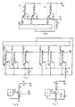
- Figs. 1, 2, 3 show three modifications of an electric circuit of the first variant of the radiation detector being claimed that uses photodiodes as sensitive elements.
- Figs. 4, 5, 6 and 7 show four modifications of an electric circuit of the second variant of the radiation detector being claimed that uses different types of sensitive elements and operates when a bias voltage, including high bias voltage, is supplied thereto.
- Figs. 8 and 9 show two modifications of an electric circuit of the third variant of the detector being claimed that uses different types of sensitive elements operating when energized by a bias voltage.
- a radiation detector being provided comprises an interrogation pulse generator 1, a radiation sensitive element 2 (a photodiode in the first variant of the detector being provided), a switching-type transistor 3 and a load 4.
- the detector may also include a current-limiting resistor 5.
- the photodiode 2 and load 4 are series-connected, with the load 4 being coupled through a signal contact with the photodiode 2 and with the common bus at the other side.
- the second electrode of the photodiode 2 is coupled with the first electrode (for example, emitter) of the switching-type transistor 3; the control electrode (for example, base) is coupled with an output of the interrogation pulse generator 1 through a resistor 6; and the third electrode of the transistor 3 (for example, a collector) is coupled with the common bus.
- An integrating capacitor 7 may be placed in parallel with the photodiode 2.
- N groups of 8 1 , 8 2 ,....8 N elements, each consisting of the series-connected switching-type transistor 3 and photodiode 2, with which the integrated capacitor 7 may be placed in parallel, is connected across the load 4.
- the interrogation pulse generator 1 comprises N outputs, each being connected to the control electrode (base) of the switching-type transistor 3 from the respective group of elements via resistor 6, where N is an integer > 1.
- N is an integer > 1.
- L loads 4 1 , 4 2 ,...4 L are included, with above-mentioned N; group of elements being placed in parallel with each i-th load, and the interrogation pulse generator 1 comprising N outputs, the number of which equals the total number of groups of elements in the detector, where L is a positive integer > 1, and N i is a positive integer.
- the second variant of the detector being provided (see Figs. 4, 5, 6, 7)
- another types of elements for example, ionization chambers (see Fig. 4) or ionizing radiation proportional counters (see Fig. 5, 6, 7) may be also used in addition to photodiodes as sensitive elements 2.
- the first simplest modification of the second variant of the detector being provided includes an interrogation pulse generator 1, a radiation sensitive element 2, a switching-type transistor 3, a load 4, a current-limiting resistor 5 and an integrating capacitor 7.
- the radiation sensitive element 2 is coupled with the supply voltage bus at one side and, via the current limiting resistor 5, with the first electrode (for example, a drain region or emitter) of the switching-type transistor 3 and the first plate of the integrating capacitor 7 at the other side, the second plate of the latter being connected to the signal contact of the load 4, the second contact of which is coupled with the common bus.
- the output of the interrogation pulse generator 1 is coupled with the control electrode (gate or base) of the switching-type transistor 3. It should be noted, that in case a bipolar transistor serves as the switching-type transistor 3, the resistor 6 is connected between the generator 1 output and transistor 3 base (see Fig. 5).
- the third electrode (for example, source or collector) of the switching-type transistor 3 is coupled with the common bus.
- a constant voltage E n of the required polarity and value is supplied to the supply voltage bus.
- Both field-effect transistors (see Fig. 4) and bipolar transistors (see Fig. 5) may be used as the switching-type transistor 3.
- N groups of 8 1 , 8 2 ,....8 N elements each consisting of a series-connected radiation-sensitive element 2 and a switching-type transistor 3, the common point of which being coupled with the signal contact of the load 4 via the integrating capacitor 7, are connected between the- supply voltage bus and common bus.
- the interrogation pulse generator 1 comprises N outputs, each being coupled with the control electrode (base) of the switching-type transistor 3 via the resistor 6 from the respective group of elements, where N is an integer > 1.
- L loads 4 1 , 4 2 ,...4 L are included with the signal output of each i-th load is connected to the above-mentioned N i groups of elements, and the interrogation pulse generator 1 contains N outputs, the number of which equals the total number of groups of elements in the detector, where L is an integer > 1 and N i is a positive integer.
- the other types of sensitive elements 2 requiring a bias voltage supply for an efficient operation may be also used in addition to photodiodes.
- the first simplest modification of the third variant of the detector being provided comprises an interrogation pulse generator 1, a radiation-sensitive element 2, a switching-type transistor 3, a load 4 and a current-limiting resistor 5.
- the radiation-sensitive element 2 is coupled at one side with the voltage supply bus and at the other side - with the first electrode (for example, drain) of the switching-type transistor 3 via the current-limiting resistor 5.
- the output of the interrogation pulse generator 1 is coupled with the control electrode (gate) of the switching-type transistor 3, the third electrode of which (for example, source) is coupled with the signal contact of the load 4 connected to the common bus at the other side.
- a constant voltage E n of the required polarity and value is delivered to the voltage supply bus.
- the second modification of the third radiation detector variant additionally comprises and integrating capacitor 7, being connected between the first electrode (for example, drain) of the switching-type transistor 3 and common bus.
- Field-effect transistors, the self-capacitance of which is used as an integrating capacitance in the first modification of said detector variant, may be used as the switching-type transistor 3 only in the third variant of the radiation detector being provided.
- the radiation detector provides the interrogation pulse generator 1 being a rectangular voltage-pulse generator.
- the amplitude and polarity of output voltage pulses are selected to enable the respective detector switching-type transistors thereby.
- Ring counters, decoders, shift registers and other devices having the number of outputs equaling those of switching-type transistors in the detector and forming the voltage pulses of the required polarity, amplitude and duration on outputs at the respective points of time may be used as the generator 1 in multi-element detector modifications.
- the generator 1 frequency sets the integrating period of the radiation recorded by the detector and defines the limit of the intensity registered.
- the current of the sensitive element 2 when exposed to radiation, integrates at the common capacitance of the sensitive element 2 and paralleled integrating capacitor 7 (see Figs. 1, 2, 3), at the capacitance of the integrating capacitor 7 (see Figs. 4-7), at the self-capacitance of the switching-type transistor 3 and integrating capacitor 7 (see Fig. 9) during the time between interrogations of the transistor 3.
- An interrogation voltage pulse with polarity activating the transistor 3 is supplied from the generator 1 output to the transistor 3 control electrode at the time the switching-type transistor 3 is being interrogated.
- the interrogation pulse generator 1 is provided with a plurality of outputs, with voltage pulses forming on each of them in a preset sequence.
- a serial interrogation of switching-type transistors 3, which are included into the groups of elements 8, corresponding, for example, to a sequential reading out of the respective integrating capacitors 7, is performed, while a sequence of current pulses, displayed as video signals, form at the load 4, when synchronizing clock is added thereto at the respective instant of time.
- the coordinate of the detector sensitive element is uniquely defined by the number of the load pulse corresponding thereto or by the time said pulse is generated, while the number of radiation particles detected in said sensitive element is defined by the amplitude of the current pulse corresponding thereto.
- the sequence of interrogation current pulses forms serially at each load at time intervals of interrogation of switching-type transistors incorporated into the groups of elements 8 coupled with said load.
- Availability of a plurality of loads in the detector allows the total number of sensitive elements to be increased in the detector without increasing the noise of amplifier integrating capacitors detecting the readout signals.
- the capability of the detector being provided to analyze space-energy characteristics of various types of radiation fields to be detected within an extensive intensity range significantly expands functional capacities and application field thereof.
- the invention may be used in the fields of nuclear physics, dosimetry, radiation flaw inspection, optics, photometry, crystallography, medicine and other fields of science and engineering.
Landscapes
- Physics & Mathematics (AREA)
- General Physics & Mathematics (AREA)
- Spectroscopy & Molecular Physics (AREA)
- Measurement Of Radiation (AREA)
- Analysing Materials By The Use Of Radiation (AREA)
- Light Receiving Elements (AREA)
Applications Claiming Priority (4)
| Application Number | Priority Date | Filing Date | Title |
|---|---|---|---|
| BY990390 | 1999-04-26 | ||
| BY19990390 | 1999-04-26 | ||
| PCT/EA2000/000002 WO2000068709A2 (ru) | 1999-04-26 | 2000-04-26 | x |
| US09/975,585 US20030071232A1 (en) | 1999-04-26 | 2001-10-12 | Radiation detector |
Publications (3)
| Publication Number | Publication Date |
|---|---|
| EP1111406A2 true EP1111406A2 (de) | 2001-06-27 |
| EP1111406A4 EP1111406A4 (de) | 2002-08-28 |
| EP1111406B1 EP1111406B1 (de) | 2004-12-22 |
Family
ID=25665745
Family Applications (1)
| Application Number | Title | Priority Date | Filing Date |
|---|---|---|---|
| EP00969049A Expired - Lifetime EP1111406B1 (de) | 1999-04-26 | 2000-04-26 | Strahlungsnachweisgerät |
Country Status (7)
| Country | Link |
|---|---|
| US (1) | US20030071232A1 (de) |
| EP (1) | EP1111406B1 (de) |
| AT (1) | ATE285586T1 (de) |
| AU (1) | AU4538300A (de) |
| DE (1) | DE60016884T2 (de) |
| EA (1) | EA001454B1 (de) |
| WO (1) | WO2000068709A2 (de) |
Families Citing this family (3)
| Publication number | Priority date | Publication date | Assignee | Title |
|---|---|---|---|---|
| FR2921154B1 (fr) * | 2007-09-14 | 2009-11-06 | Commissariat Energie Atomique | Dispositif de detection d'un rayonnement electromagnetique a limitation de courant |
| CN107765289B (zh) * | 2017-11-06 | 2024-06-25 | 天津大学 | 基于柔性pin二极管的辐照强度检测器 |
| CN112285436A (zh) * | 2020-11-08 | 2021-01-29 | 湖南省福晶电子有限公司 | 一种电子元件用的辐射检测系统 |
Family Cites Families (9)
| Publication number | Priority date | Publication date | Assignee | Title |
|---|---|---|---|---|
| GB1169663A (en) * | 1967-09-06 | 1969-11-05 | Commissariat Energie Atomique | Integrated Photosensitive Circuit |
| SU532016A1 (ru) * | 1974-04-08 | 1976-10-15 | Предприятие П/Я А-1001 | Устройство дл регистрации светового потока |
| DD129683B1 (de) * | 1977-01-31 | 1980-10-01 | Pentacon Dresden Veb | Belichtungsmessschaltung |
| SU715944A1 (ru) * | 1977-06-23 | 1980-02-15 | Научно-производственное объединение "Нефтехимавтоматика" | Фотоэлектронное устройство |
| DE2936492A1 (de) * | 1979-09-10 | 1981-03-26 | Siemens AG, 1000 Berlin und 8000 München | Analog-digital-wandler zur bewertung des ausgangssignals eines optoelektronischen sensorelements |
| JPS5651166A (en) * | 1979-10-03 | 1981-05-08 | Hitachi Ltd | Solid image pickup device |
| SU1662215A1 (ru) * | 1989-08-07 | 1995-08-20 | Институт Физики Полупроводников Со Ан Ссср | Преобразователь интенсивности света в частоту |
| JP2953297B2 (ja) * | 1994-03-30 | 1999-09-27 | 日本電気株式会社 | 受光素子およびその駆動方法 |
| JPH10185681A (ja) * | 1996-11-08 | 1998-07-14 | Mitsuteru Kimura | 熱型赤外線センサとその製造方法およびこれを用いた赤外線イメージセンサ |
-
2000
- 2000-03-16 EA EA200000382A patent/EA001454B1/ru not_active IP Right Cessation
- 2000-04-26 DE DE60016884T patent/DE60016884T2/de not_active Expired - Fee Related
- 2000-04-26 EP EP00969049A patent/EP1111406B1/de not_active Expired - Lifetime
- 2000-04-26 AU AU45383/00A patent/AU4538300A/en not_active Abandoned
- 2000-04-26 WO PCT/EA2000/000002 patent/WO2000068709A2/ru not_active Ceased
- 2000-04-26 AT AT00969049T patent/ATE285586T1/de not_active IP Right Cessation
-
2001
- 2001-10-12 US US09/975,585 patent/US20030071232A1/en not_active Abandoned
Also Published As
| Publication number | Publication date |
|---|---|
| EA200000382A3 (ru) | 2001-02-26 |
| AU4538300A (en) | 2000-11-21 |
| WO2000068709A2 (ru) | 2000-11-16 |
| EA200000382A2 (ru) | 2000-10-30 |
| DE60016884T2 (de) | 2005-12-29 |
| EP1111406B1 (de) | 2004-12-22 |
| DE60016884D1 (de) | 2005-01-27 |
| ATE285586T1 (de) | 2005-01-15 |
| EP1111406A4 (de) | 2002-08-28 |
| EA001454B1 (ru) | 2001-04-23 |
| WO2000068709A3 (ru) | 2001-04-12 |
| US20030071232A1 (en) | 2003-04-17 |
Similar Documents
| Publication | Publication Date | Title |
|---|---|---|
| US7411198B1 (en) | Integrator circuitry for single channel radiation detector | |
| JP2011174936A (ja) | 放射線撮像のための撮像素子 | |
| Huber et al. | Characterization of a 64 channel PET detector using photodiodes for crystal identification | |
| US11041965B2 (en) | Radiation-detecting device | |
| EP1111406B1 (de) | Strahlungsnachweisgerät | |
| CN107450092B (zh) | 用于测量光子信息的装置 | |
| Sadigov et al. | A micropixel avalanche phototransistor for time of flight measurements | |
| TW201826549A (zh) | 光子檢測器 | |
| US20070007463A1 (en) | Device and method for the measurement of depth of interaction using co-planar electrodes | |
| Giha et al. | Readout electronics of a handheld dual particle imager | |
| CA2189699C (en) | Three terminal ion chambers | |
| EP3644097B1 (de) | Optischer detektor und optische detektionsvorrichtung | |
| Massari et al. | Low-power charge division circuits for wireless applications based on silicon photomultipliers | |
| Dabrowski et al. | A readout system for position sensitive measurements of X-ray using silicon strip detectors | |
| Luu et al. | LED Optical Fiber Profile investigations and Cosmic ray Muons detections with 4x4 MPPC arrays | |
| Zhang et al. | Improving the performance of small planar detectors for dedicated PET instruments | |
| CN111694043B (zh) | 光子测量装置及光子测量设备 | |
| Beznosko | Novel multi-pixel silicon photon detectors and applications in T2K | |
| CZ2001283A3 (cs) | Detektor záření | |
| US11726219B2 (en) | Multimodal photon and neutron imaging devices with fast event-by-event multisampling readout and optimized particle type discrimination | |
| Estrada et al. | Readout electronics in large detector matrix for soft X-ray in medical applications | |
| El-Azm et al. | Investigating the response of single pad and hybrid pixel detectors (Si, GaAs, CdTe, CZT) for 226Ra and 137Cs | |
| Belkacem et al. | PRELIMINARY DESIGN AND SIMULATION OF SIPM DEVICE OPERATION FOR A POTENTIAL CUBESAT RADIATION DETECTOR | |
| Lerche et al. | 5 PET Front-End Electronics | |
| US7732749B2 (en) | System and method for measuring the output of a photodetector and for reducing sensitivity to temperature variations |
Legal Events
| Date | Code | Title | Description |
|---|---|---|---|
| PUAI | Public reference made under article 153(3) epc to a published international application that has entered the european phase |
Free format text: ORIGINAL CODE: 0009012 |
|
| 17P | Request for examination filed |
Effective date: 20010126 |
|
| AK | Designated contracting states |
Kind code of ref document: A2 Designated state(s): AT BE CH CY DE DK ES FI FR GB GR IE IT LI LU MC NL PT SE |
|
| AX | Request for extension of the european patent |
Free format text: AL;LT;LV;MK;RO;SI |
|
| RAP1 | Party data changed (applicant data changed or rights of an application transferred) |
Owner name: SV GROUP S.R.O. |
|
| RIN1 | Information on inventor provided before grant (corrected) |
Inventor name: SV GROUP S.R.O. |
|
| RIN1 | Information on inventor provided before grant (corrected) |
Inventor name: KOZUS, VIKTOR IVANOVICH Inventor name: DANILOV, VYACHESLAV ALEXANDROVICH |
|
| TCNL | Nl: translation of patent claims filed |
Owner name: KONINKLIJKE PHILIPS ELECTRONICS N.V. |
|
| A4 | Supplementary search report drawn up and despatched |
Effective date: 20020717 |
|
| AK | Designated contracting states |
Kind code of ref document: A4 Designated state(s): AT BE CH CY DE DK ES FI FR GB GR IE IT LI LU MC NL PT SE |
|
| RIC1 | Information provided on ipc code assigned before grant |
Free format text: 7G 01T 1/00 A, 7G 01J 5/24 B, 7G 01J 1/44 B |
|
| 17Q | First examination report despatched |
Effective date: 20021127 |
|
| GRAP | Despatch of communication of intention to grant a patent |
Free format text: ORIGINAL CODE: EPIDOSNIGR1 |
|
| GRAS | Grant fee paid |
Free format text: ORIGINAL CODE: EPIDOSNIGR3 |
|
| GRAA | (expected) grant |
Free format text: ORIGINAL CODE: 0009210 |
|
| AK | Designated contracting states |
Kind code of ref document: B1 Designated state(s): AT BE CH CY DE DK ES FI FR GB GR IE IT LI LU MC NL PT SE |
|
| PG25 | Lapsed in a contracting state [announced via postgrant information from national office to epo] |
Ref country code: FI Free format text: LAPSE BECAUSE OF FAILURE TO SUBMIT A TRANSLATION OF THE DESCRIPTION OR TO PAY THE FEE WITHIN THE PRESCRIBED TIME-LIMIT Effective date: 20041222 Ref country code: IT Free format text: LAPSE BECAUSE OF FAILURE TO SUBMIT A TRANSLATION OF THE DESCRIPTION OR TO PAY THE FEE WITHIN THE PRESCRIBED TIME-LIMIT;WARNING: LAPSES OF ITALIAN PATENTS WITH EFFECTIVE DATE BEFORE 2007 MAY HAVE OCCURRED AT ANY TIME BEFORE 2007. THE CORRECT EFFECTIVE DATE MAY BE DIFFERENT FROM THE ONE RECORDED. Effective date: 20041222 Ref country code: BE Free format text: LAPSE BECAUSE OF FAILURE TO SUBMIT A TRANSLATION OF THE DESCRIPTION OR TO PAY THE FEE WITHIN THE PRESCRIBED TIME-LIMIT Effective date: 20041222 Ref country code: CH Free format text: LAPSE BECAUSE OF FAILURE TO SUBMIT A TRANSLATION OF THE DESCRIPTION OR TO PAY THE FEE WITHIN THE PRESCRIBED TIME-LIMIT Effective date: 20041222 Ref country code: FR Free format text: LAPSE BECAUSE OF FAILURE TO SUBMIT A TRANSLATION OF THE DESCRIPTION OR TO PAY THE FEE WITHIN THE PRESCRIBED TIME-LIMIT Effective date: 20041222 Ref country code: LI Free format text: LAPSE BECAUSE OF FAILURE TO SUBMIT A TRANSLATION OF THE DESCRIPTION OR TO PAY THE FEE WITHIN THE PRESCRIBED TIME-LIMIT Effective date: 20041222 |
|
| REG | Reference to a national code |
Ref country code: GB Ref legal event code: FG4D |
|
| REG | Reference to a national code |
Ref country code: CH Ref legal event code: EP |
|
| RAP2 | Party data changed (patent owner data changed or rights of a patent transferred) |
Owner name: TROFIMENKO, VLADIMIR Owner name: TRIGUB, VLADIMIR |
|
| REG | Reference to a national code |
Ref country code: IE Ref legal event code: FG4D |
|
| REF | Corresponds to: |
Ref document number: 60016884 Country of ref document: DE Date of ref document: 20050127 Kind code of ref document: P |
|
| PG25 | Lapsed in a contracting state [announced via postgrant information from national office to epo] |
Ref country code: SE Free format text: LAPSE BECAUSE OF FAILURE TO SUBMIT A TRANSLATION OF THE DESCRIPTION OR TO PAY THE FEE WITHIN THE PRESCRIBED TIME-LIMIT Effective date: 20050322 Ref country code: DK Free format text: LAPSE BECAUSE OF FAILURE TO SUBMIT A TRANSLATION OF THE DESCRIPTION OR TO PAY THE FEE WITHIN THE PRESCRIBED TIME-LIMIT Effective date: 20050322 Ref country code: GR Free format text: LAPSE BECAUSE OF FAILURE TO SUBMIT A TRANSLATION OF THE DESCRIPTION OR TO PAY THE FEE WITHIN THE PRESCRIBED TIME-LIMIT Effective date: 20050322 |
|
| NLT2 | Nl: modifications (of names), taken from the european patent patent bulletin |
Owner name: TROFIMENKO, VLADIMIR EN TRIGUB, VLADIMIR |
|
| PG25 | Lapsed in a contracting state [announced via postgrant information from national office to epo] |
Ref country code: ES Free format text: LAPSE BECAUSE OF FAILURE TO SUBMIT A TRANSLATION OF THE DESCRIPTION OR TO PAY THE FEE WITHIN THE PRESCRIBED TIME-LIMIT Effective date: 20050402 |
|
| PGFP | Annual fee paid to national office [announced via postgrant information from national office to epo] |
Ref country code: AT Payment date: 20050421 Year of fee payment: 6 |
|
| PG25 | Lapsed in a contracting state [announced via postgrant information from national office to epo] |
Ref country code: LU Free format text: LAPSE BECAUSE OF NON-PAYMENT OF DUE FEES Effective date: 20050426 Ref country code: IE Free format text: LAPSE BECAUSE OF NON-PAYMENT OF DUE FEES Effective date: 20050426 Ref country code: CY Free format text: LAPSE BECAUSE OF FAILURE TO SUBMIT A TRANSLATION OF THE DESCRIPTION OR TO PAY THE FEE WITHIN THE PRESCRIBED TIME-LIMIT Effective date: 20050426 |
|
| PG25 | Lapsed in a contracting state [announced via postgrant information from national office to epo] |
Ref country code: MC Free format text: LAPSE BECAUSE OF NON-PAYMENT OF DUE FEES Effective date: 20050430 |
|
| REG | Reference to a national code |
Ref country code: CH Ref legal event code: PL |
|
| REG | Reference to a national code |
Ref country code: GB Ref legal event code: 732E |
|
| PLBE | No opposition filed within time limit |
Free format text: ORIGINAL CODE: 0009261 |
|
| STAA | Information on the status of an ep patent application or granted ep patent |
Free format text: STATUS: NO OPPOSITION FILED WITHIN TIME LIMIT |
|
| 26N | No opposition filed |
Effective date: 20050923 |
|
| EN | Fr: translation not filed | ||
| PGFP | Annual fee paid to national office [announced via postgrant information from national office to epo] |
Ref country code: NL Payment date: 20060419 Year of fee payment: 7 |
|
| PG25 | Lapsed in a contracting state [announced via postgrant information from national office to epo] |
Ref country code: AT Free format text: LAPSE BECAUSE OF NON-PAYMENT OF DUE FEES Effective date: 20060426 |
|
| PGFP | Annual fee paid to national office [announced via postgrant information from national office to epo] |
Ref country code: GB Payment date: 20060426 Year of fee payment: 7 |
|
| GBPC | Gb: european patent ceased through non-payment of renewal fee |
Effective date: 20070426 |
|
| NLV4 | Nl: lapsed or anulled due to non-payment of the annual fee |
Effective date: 20071101 |
|
| PG25 | Lapsed in a contracting state [announced via postgrant information from national office to epo] |
Ref country code: PT Free format text: LAPSE BECAUSE OF NON-PAYMENT OF DUE FEES Effective date: 20050522 |
|
| PG25 | Lapsed in a contracting state [announced via postgrant information from national office to epo] |
Ref country code: NL Free format text: LAPSE BECAUSE OF NON-PAYMENT OF DUE FEES Effective date: 20071101 |
|
| PGFP | Annual fee paid to national office [announced via postgrant information from national office to epo] |
Ref country code: DE Payment date: 20071031 Year of fee payment: 8 |
|
| PG25 | Lapsed in a contracting state [announced via postgrant information from national office to epo] |
Ref country code: GB Free format text: LAPSE BECAUSE OF NON-PAYMENT OF DUE FEES Effective date: 20070426 |
|
| PG25 | Lapsed in a contracting state [announced via postgrant information from national office to epo] |
Ref country code: DE Free format text: LAPSE BECAUSE OF NON-PAYMENT OF DUE FEES Effective date: 20081101 |