EP1109163A2 - Optical device - Google Patents
Optical device Download PDFInfo
- Publication number
- EP1109163A2 EP1109163A2 EP00127242A EP00127242A EP1109163A2 EP 1109163 A2 EP1109163 A2 EP 1109163A2 EP 00127242 A EP00127242 A EP 00127242A EP 00127242 A EP00127242 A EP 00127242A EP 1109163 A2 EP1109163 A2 EP 1109163A2
- Authority
- EP
- European Patent Office
- Prior art keywords
- light receiving
- light
- receiving element
- wavelength
- area
- Prior art date
- Legal status (The legal status is an assumption and is not a legal conclusion. Google has not performed a legal analysis and makes no representation as to the accuracy of the status listed.)
- Granted
Links
Images











Classifications
-
- G—PHYSICS
- G11—INFORMATION STORAGE
- G11B—INFORMATION STORAGE BASED ON RELATIVE MOVEMENT BETWEEN RECORD CARRIER AND TRANSDUCER
- G11B7/00—Recording or reproducing by optical means, e.g. recording using a thermal beam of optical radiation by modifying optical properties or the physical structure, reproducing using an optical beam at lower power by sensing optical properties; Record carriers therefor
- G11B7/12—Heads, e.g. forming of the optical beam spot or modulation of the optical beam
- G11B7/13—Optical detectors therefor
- G11B7/131—Arrangement of detectors in a multiple array
-
- G—PHYSICS
- G11—INFORMATION STORAGE
- G11B—INFORMATION STORAGE BASED ON RELATIVE MOVEMENT BETWEEN RECORD CARRIER AND TRANSDUCER
- G11B7/00—Recording or reproducing by optical means, e.g. recording using a thermal beam of optical radiation by modifying optical properties or the physical structure, reproducing using an optical beam at lower power by sensing optical properties; Record carriers therefor
- G11B7/08—Disposition or mounting of heads or light sources relatively to record carriers
- G11B7/09—Disposition or mounting of heads or light sources relatively to record carriers with provision for moving the light beam or focus plane for the purpose of maintaining alignment of the light beam relative to the record carrier during transducing operation, e.g. to compensate for surface irregularities of the latter or for track following
- G11B7/0901—Disposition or mounting of heads or light sources relatively to record carriers with provision for moving the light beam or focus plane for the purpose of maintaining alignment of the light beam relative to the record carrier during transducing operation, e.g. to compensate for surface irregularities of the latter or for track following for track following only
- G11B7/0903—Multi-beam tracking systems
-
- G—PHYSICS
- G11—INFORMATION STORAGE
- G11B—INFORMATION STORAGE BASED ON RELATIVE MOVEMENT BETWEEN RECORD CARRIER AND TRANSDUCER
- G11B7/00—Recording or reproducing by optical means, e.g. recording using a thermal beam of optical radiation by modifying optical properties or the physical structure, reproducing using an optical beam at lower power by sensing optical properties; Record carriers therefor
- G11B7/08—Disposition or mounting of heads or light sources relatively to record carriers
- G11B7/09—Disposition or mounting of heads or light sources relatively to record carriers with provision for moving the light beam or focus plane for the purpose of maintaining alignment of the light beam relative to the record carrier during transducing operation, e.g. to compensate for surface irregularities of the latter or for track following
- G11B7/0908—Disposition or mounting of heads or light sources relatively to record carriers with provision for moving the light beam or focus plane for the purpose of maintaining alignment of the light beam relative to the record carrier during transducing operation, e.g. to compensate for surface irregularities of the latter or for track following for focusing only
- G11B7/0912—Disposition or mounting of heads or light sources relatively to record carriers with provision for moving the light beam or focus plane for the purpose of maintaining alignment of the light beam relative to the record carrier during transducing operation, e.g. to compensate for surface irregularities of the latter or for track following for focusing only by push-pull method
-
- G—PHYSICS
- G11—INFORMATION STORAGE
- G11B—INFORMATION STORAGE BASED ON RELATIVE MOVEMENT BETWEEN RECORD CARRIER AND TRANSDUCER
- G11B7/00—Recording or reproducing by optical means, e.g. recording using a thermal beam of optical radiation by modifying optical properties or the physical structure, reproducing using an optical beam at lower power by sensing optical properties; Record carriers therefor
- G11B7/12—Heads, e.g. forming of the optical beam spot or modulation of the optical beam
- G11B7/123—Integrated head arrangements, e.g. with source and detectors mounted on the same substrate
-
- G—PHYSICS
- G11—INFORMATION STORAGE
- G11B—INFORMATION STORAGE BASED ON RELATIVE MOVEMENT BETWEEN RECORD CARRIER AND TRANSDUCER
- G11B7/00—Recording or reproducing by optical means, e.g. recording using a thermal beam of optical radiation by modifying optical properties or the physical structure, reproducing using an optical beam at lower power by sensing optical properties; Record carriers therefor
- G11B7/12—Heads, e.g. forming of the optical beam spot or modulation of the optical beam
- G11B7/125—Optical beam sources therefor, e.g. laser control circuitry specially adapted for optical storage devices; Modulators, e.g. means for controlling the size or intensity of optical spots or optical traces
- G11B7/127—Lasers; Multiple laser arrays
- G11B7/1275—Two or more lasers having different wavelengths
-
- G—PHYSICS
- G11—INFORMATION STORAGE
- G11B—INFORMATION STORAGE BASED ON RELATIVE MOVEMENT BETWEEN RECORD CARRIER AND TRANSDUCER
- G11B7/00—Recording or reproducing by optical means, e.g. recording using a thermal beam of optical radiation by modifying optical properties or the physical structure, reproducing using an optical beam at lower power by sensing optical properties; Record carriers therefor
- G11B7/12—Heads, e.g. forming of the optical beam spot or modulation of the optical beam
- G11B7/135—Means for guiding the beam from the source to the record carrier or from the record carrier to the detector
- G11B7/1353—Diffractive elements, e.g. holograms or gratings
-
- G—PHYSICS
- G11—INFORMATION STORAGE
- G11B—INFORMATION STORAGE BASED ON RELATIVE MOVEMENT BETWEEN RECORD CARRIER AND TRANSDUCER
- G11B7/00—Recording or reproducing by optical means, e.g. recording using a thermal beam of optical radiation by modifying optical properties or the physical structure, reproducing using an optical beam at lower power by sensing optical properties; Record carriers therefor
- G11B2007/0003—Recording, reproducing or erasing systems characterised by the structure or type of the carrier
- G11B2007/0006—Recording, reproducing or erasing systems characterised by the structure or type of the carrier adapted for scanning different types of carrier, e.g. CD & DVD
Definitions
- the present invention relates to an optical device for use in a reading apparatus of an optical information recording medium such as an optical disc, and more particularly, it relates to an optical device which is suitable for a compatible reproduction system of a DVD (known as "Digital Versatile Disc” or “Digital Video Disc”) and a compact disc-write once (CD-R) and which can be miniaturized.
- a compatible reproduction system of a DVD known as "Digital Versatile Disc” or “Digital Video Disc”
- CD-R compact disc-write once
- the reflectance of a recording medium has a large dependence on wavelength, and hence, a laser light source of a 780 nm band different from a 650 nm band for a DVD is essential, and a pickup optical system having a built-in light source of two wavelengths is necessary.
- a device obtained by mechanically coupling two conventional and independent pickups a device obtained by independently attaching received/emitted light integration elements for wavelengths, synthesizing them on one optical axis by a dichroic prism, and sharing a partial optical system such as an objective lens, and the like.
- another device has been proposed which can be obtained by receiving, in one package, two semiconductor laser chips different in wavelength from each other, setting other components to be independent of one another but setting the optical axis to be common.
- Figs.1A and 1B are explanatory views showing the focus error detection by the aforementioned spot size detection (SSD) method (Japanese Patent Application Laid-Open No. 101417/1993). More specifically, Fig.1A is a schematic side view of an apparatus for performing the focus error detection, and Fig.1B is a schematic plan view of a photodiode for detecting the diffracted light in the apparatus.
- SSD spot size detection
- a reflected light reflected by an optical disc 357 is transmitted through an objective lens 356 and separated into a pair of conjugate lights b1, b1' by a holographic optical element 355.
- the holographic optical element 355 is constituted in such a manner that the conjugate light bl is focused above a light receiving element substrate 350, and the conjugate light b1' is focused below the substrate 350.
- the respective conjugate lights b1, b1' are received by photo detection diodes 352 and 353 disposed in the light receiving element substrate 350.
- the photo detection diodes 352 and 353 are divided into three areas 352a, 352b, 352c and 353a, 353b, 353c in Y direction crossing at right angles to X direction in which the conjugate lights b1 and b1' are separated.
- a spot S1 on the photo detection diode 352 becomes the same in size as a spot S2 on the photo detection diode 353, and the focus error signal FE of the equation (1) turns to zero.
- the focus error signal FE of the equation (1) indicates a positive or negative value other than zero. Therefore, a polarity of the focus error signal FE is reversed before and after a focusing point. Therefore, by detecting the focus error signal FE, focus adjustment of the laser light with respect to the optical disc 357 can be performed.
- the diffraction angle and other characteristics are determined by a mathematical relation between a period structure and light wavelength, and therefore the diffraction angle largely changes with respect to different wavelengths.
- spot size detection method as the focus error detection method suitable for the integrated device using the holographic optical element, it is essential to dispose a photodetector light receiving surface for detecting the holographic optical element diffracted light in the very vicinity of the conjugate point of the semiconductor laser light emitting point.
- an optimum photodetector light receiving surface position largely differs by the characteristic change.
- tracking error detection of a differential push-pull (DPP) system is preferable, but in an integrated pickup using hologram or the like to satisfy small size, high rate and low cost, it has been difficult to realize the tracking error detection of the DPP method for the DVD-RAM without causing cost up or performance deterioration.
- DPP differential push-pull
- an object of the present invention is to provide an optical device which realizes complementary focus error detection with respect to two wavelengths in an optical system using lights of two wavelengths.
- an optical device for reading information from an information recording medium, comprising: a first light source for outputting a light of a first wavelength; a second light source for outputting a light of a second wavelength; a holographic optical element having a first diffraction area and a second diffraction area for diffracting the lights of the first and second wavelengths; and a light receiving element substrate provided with a first light receiving element and a second light receiving element for receiving a diffracted light from the holographic optical element, wherein the first diffraction area and the second diffraction area have grating arrangements whose grating axis directions are parallel to each other and whose grating pitches are different from each other, light emitting points of the first and second light sources are apart from each other by a predetermined distance in a direction crossing at right angles to the grating axis, the grating pitches of the first diffraction area and the second dif
- a focus error signal is obtained on the basis of signals from the first light receiving element and the second light receiving element.
- the diffracted lights to the first and second positions are both + 1st order diffracted lights by the first diffraction area and the second diffraction area, and the interval between the light emitting points of the first and second light sources and the grating pitches of the first diffraction area and the second diffraction area are set in such a manner that - 1st order diffracted lights of the first wavelength and the second wavelength by the first diffraction area and the second diffraction area are converged to third, fourth, fifth, sixth positions apart from one another by a predetermined interval capable of receiving the lights in independent light receiving areas not superposed to one another on the light receiving element substrate.
- the - 1st order diffracted lights of the first wavelength by the first diffraction area and the second diffraction area are converged to the third and fourth positions
- the - 1st order diffracted lights of the second wavelength by the first diffraction area and the second diffraction area are converged to the fifth and sixth positions
- a tracking error signal for the first wavelength is obtained on the basis of detection signals from the light receiving elements disposed in the third and fourth positions
- a tracking error signal for the second wavelength is obtained on the basis of the signals from the light receiving elements disposed in the fifth and sixth positions or the signals from the light receiving elements disposed on both side areas opposite to each other in a grating axis direction of the fifth or sixth position.
- the tracking error signal for the second wavelength is obtained on the basis of the signals from the light receiving elements disposed in the fifth and sixth positions.
- an optical device for reading information from an information recording medium, comprising: a first light source for outputting a light of a first wavelength; a second light source for outputting a light of a second wavelength; a holographic optical element having a first diffraction area and a second diffraction area for diffracting the lights of the first and second wavelengths; and a light receiving element substrate provided with a first light receiving element and a second light receiving element for receiving a diffracted light from the holographic optical element, wherein in the first diffraction area and the second diffraction area, grating pitches are identical with each other, grating axis directions are different from each other by a predetermined angle of 30° or less, and light emitting points of the first and second light sources are apart from each other by a predetermined distance in a direction substantially crossing at right angles to the grating axis direction, the grating pitches of the first
- a focus error signal is obtained on the basis of signals from the first light receiving element and the second light receiving element.
- the diffracted lights to the first and second positions are both + 1st order diffracted lights by the first diffraction area and the second diffraction area
- a tracking error signal of the first wavelength light is obtained on the basis of signals from the light receiving elements disposed in the third and fourth positions in which the - 1st order diffracted lights of the first wavelength by the first diffraction area and the second diffraction area are converged on the light receiving element substrate
- a tracking error signal of the second wavelength light is obtained on the basis of the signals from the light receiving elements disposed in the fifth and sixth positions in which the - 1st order diffracted light of the second wavelength by the first diffraction area or the second diffraction area is converged on the light receiving element substrate or the signals from the light receiving elements disposed on both side areas opposite to each other in a grating axis direction of the fifth position or the sixth position.
- the tracking error signal for the second wavelength is obtained on the basis of the signals from the light receiving elements disposed in the fifth and sixth positions.
- the first light receiving element and the second light receiving element are divided into a plurality of sub areas by a plurality of division lines, and the focus error signal is obtained on the basis of the signals from the plurality of sub areas.
- a point at which the 0th order transmitted light intersects the light receiving element substrate is P
- an angle formed by a radial axis defined in a radial direction crossing at right angles to a track of the information recording medium and a straight line connecting the first or second position to the intersection point P is ⁇ 1
- an angle formed by the radial axis and the plurality of division lines is ⁇ 2
- a relation of 0 ⁇ ⁇ 2 ⁇ ⁇ 1 is satisfied.
- an optical device for using a laser light having a predetermined wavelength to read information from an information recording medium, comprising: a laser light source for generating the laser light; a light receiving element substrate provided with a plurality of light receiving areas in the same plane; a 3-beam generating diffraction grating for branching the laser light from the laser light source to three emitted lights; and a holographic optical element, divided into at least a first area and a second area in the same plane, for branching a reflected light from the information recording medium and turning the light to the light receiving element substrate, wherein diffraction axes of the first area and the second area are formed in such a manner that a diffraction axis direction of ⁇ 1st order diffracted lights by the first area and the diffraction axis direction of the ⁇ 1st order diffracted lights by the second area form predetermined angles in opposite directions with respect to
- a focus error signal is obtained on the basis of signals from a first light receiving element and a second light receiving element disposed in a first position in which the diffracted light diffracted by the first diffraction area is converged on the light receiving element substrate and a second position in which the diffracted light diffracted by the second diffraction area is converged on the light receiving element substrate, respectively.
- the diffracted lights to the first and second positions are both + 1st order diffracted lights by the first diffraction area and the second diffraction area
- a tracking error signal is obtained on the basis of signals from the light receiving elements disposed in the third and fourth positions in which - 1st order diffracted lights by the first diffraction area and the second diffraction area are converged on the light receiving element substrate, and the signals from four light receiving elements, disposed on the light receiving element substrate, for detecting the + 1st order diffracted light of the second side beam by the first area, the + 1st order diffracted light of the second side beam by the second area, the - 1st order diffracted light of the second side beam by the first area, and the - 1st order diffracted light of the second side beam by the second area, respectively.
- Fig.2 is a perspective view of a first embodiment of an optical device of the present invention
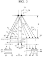
- Fig.3 is an explanatory view showing a light trace or the like of a diffracted light in the first embodiment.
- an optical device 23 of the first embodiment is used in an optical pickup for reading information from an information recording medium 21 such as a DVD or CD, and provided with a first light source 25 for outputting a light of a first wavelength ⁇ 1, and a second light source 27 for outputting a light of a second wavelength ⁇ 2.
- the first wavelength ⁇ 1 is, for example, 650 nm for the DVD
- the second wavelength ⁇ 2 is, for example, 780 nm for the CD.
- the first light source 25 is apart from the second light source 27 by a predetermined distance d in a direction (X axis direction) crossing at right angles to a grating axis direction (Y axis direction) of a holographic optical element described later.
- Fig.3 shows conjugate points C1, C2 of light emitting points of the light sources 25, 27.
- the conjugate points C1, C2 show image positions of the light emitting points of the first and second light sources 25, 27 by a reflection mirror 41 shown in Fig.2.
- the optical device 23 is further provided with a holographic optical element 33 including a first diffraction area 29 and a second diffraction area 31 for diffracting the lights of the first and second wavelengths reflected by the information recording medium 21.
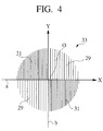
- the first diffraction area 29 and second diffraction area 31 of the holographic optical element 33 are formed in positions present in a pair of diagonal directions and positions present in another pair of diagonal directions when a circular area on a substrate (not shown) of the holographic optical element 33 is divided by a straight line a extending along X axis direction and a straight line b extending along Y axis direction.
- a grating pitch ⁇ 1 of the first diffraction area 29 is set to be larger than a grating pitch ⁇ 2 of the second diffraction area 31. Therefore, when one wavelength light is incident, a diffraction angle of the diffracted light by the first diffraction area 29 becomes smaller than the diffraction angle of the diffracted light (of the same dimension) by the second diffraction area 31.
- optical axes A1, A2 determined by 0th order transmitted lights of the first and second wavelengths ⁇ 1, ⁇ 2 go through the conjugate points C1, C2 and extend at right angles to both X and Y axes.
- the grating pitches ⁇ 1, ⁇ 2 of the first diffraction area 29 and second diffraction area 31 are determined to satisfy the following two conditions.
- substantially equal (the same) preferably means “equal (the same) with an error of 50 ⁇ m or less", more preferably means “equal (the same) with an error of 20 ⁇ m or less”, and further preferably means “equal (the same) with an error of about 1 ⁇ m”.
- an interval h between the light receiving element substrate 39 and the holographic optical element 33 is, for example, 3000 ⁇ m, and the distance d is set, for example, to about 100 ⁇ m, ⁇ 1 and ⁇ 2 are set, for example, to about 4 ⁇ m and 3.3 ⁇ m, respectively.
- the light with the first wavelength ⁇ 1 from the first light source 25 is reflected by the information recording medium 21, and then diffracted by the first and second diffraction areas 29, 31 to generate the first and second diffracted lights r11, r12 Subsequently, the diffracted light r11 is converted to the first position P1 on the light receiving element substrate 39, and the diffracted light r12 is converged to the second position P2 on the light receiving element substrate 39.
- the distance between the first position P1 and the second position P2 is about 100 ⁇ m.
- the light with the second wavelength ⁇ 2 from the second light source 27 is reflected by the information recording medium 21, and subsequently diffracted by the first and second diffraction areas 29, 31 to produce the first and second diffracted lights r21, r22.
- the first diffracted light r21 is converged to the first position P1 on the light receiving element substrate 39 in an error range of about 10 ⁇ m
- the second diffracted light r22 is converged to the second position P2 on the light receiving element substrate 39 in the error range of about 10 ⁇ m.
- a first light receiving element 35 and a second light receiving element 37 each having a width of about 100 ⁇ m in X axis direction are disposed in the first position P1 and second position P2. Therefore, the diffracted lights r11, r21 are both converged onto the first light receiving element 35, and the diffracted lights r12, r22 are both converged onto the second light receiving element 37.
- a lens power is applied to the first diffraction area 29 and second diffraction area 31, the lens power is applied in such a manner that a concave lens acts on the diffracted lights r11, r21, and a convex lens acts on the diffracted lights r12, r22. Therefore, based on outputs from the first light receiving element 35 and second light receiving element 37, a focus error signal by a complementary spot size detection method can be obtained.
- a third light receiving element 43, fourth light receiving element 45, fifth light receiving element 47, sixth light receiving element 49 each having a width of about 100 ⁇ m in the X axis direction are disposed in the third position P3, fourth position P4, fifth position P5, and sixth position P6.
- the - 1st order diffracted lights r11', r12', r21', r22' of the first and second wavelengths are converged onto the third light receiving element 43, fourth light receiving element 45, fifth light receiving element 47, and sixth light receiving element 49, respectively.
- the tracking error signal of a CD-R luminous flux can be obtained.
- a 3-beam generating diffraction grating (not shown) is disposed between the second light source 27 and the information recording medium 21.
- This 3-beam generating diffraction grating can be disposed, for example, on a surface opposite to a surface on which the holographic optical element 31 is disposed in a diffraction element substrate (not shown) provided with the holographic optical element 31.
- a seventh light receiving element 51 and an eighth light receiving element 53 are disposed on both sides of the first and second light receiving elements 35, 37.
- ninth and tenth light receiving elements 55, 57 are disposed on both sides of the fifth and sixth light receiving elements 47, 49.
- the CD luminous flux emitted from the second light source 27 is branched to three luminous fluxes arranged in a tangential direction (Y axis direction) of the information recording medium 21 by the 3-beam generating diffraction grating (not shown).
- a grating depth for example, to 650 nm for phase modulation of 2 n ⁇
- a diffraction action is advantageously generated.
- the three luminous fluxes are reflected by the information recording medium 21, then diffracted by the first and second diffraction areas 29, 31, diffracted with the same diffraction angle as that of the diffracted lights r21, r22, r21', r22', and converged onto the light receiving elements 55, 47(49), 57 or the light receiving elements 51, 35(37), 53 arranged in the Y axis direction on the light receiving element substrate 39. Therefore, based on outputs from the light receiving elements 51, 53, 55, 57, the tracking error signal of the CD luminous flux by the 3-beam method can be obtained.
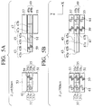
- Figs.5A and 5B show detailed constitution and action of the first and second light receiving elements 35, 37, and the third to tenth light receiving elements 43 to 57.
- Fig.5A shows a relation between the respective light receiving elements and respective diffracted light spots when the diffracted lights r11, r12, r11', r12' having the first wavelength ⁇ 1 are incident upon the first to tenth light receiving elements 35, 37, 43 to 57
- Fig.5B shows the relation between the respective light receiving elements and the respective diffracted light spots when the diffracted lights r21, r22, r21', r22' having the second wavelength ⁇ 2 are incident upon the respective light receiving elements.
- the first light receiving element 35 is divided into three light receiving areas 35a, 35b, 35c in the Y axis direction, and the second light receiving element 37 is similarly divided into light receiving areas 37a, 37b, 37c.
- the third light receiving element 43 is divided into light receiving areas 43a, 43b in the Y axis direction
- the fourth light receiving element 45, fifth light receiving element 47 and sixth light receiving element 49 are similarly divided into light receiving areas 45a, 45b, light receiving areas 47a, 47b and light receiving areas 49a, 49b, respectively.
- crosshatch marks 59 on the light receiving element represent spots of the diffracted lights r11, r11' by the first diffraction area 29.
- hatch marks 61 represent the spots of the diffracted lights r12, r12' by the second diffraction area 31.
- the focus error signal of the DVD luminous flux having the first wavelength can be obtained.
- the tracking error signal to the information recording medium 21 of the DVD luminous flux of the first wavelength can be computed/detected based on detection signals from the light receiving areas 43a, 43b, 45a, 45b having the spot marks 59, 61 of the diffracted lights r11 , , r12'. More specifically, provided the outputs of the light receiving areas 43a, 45a, 43b, 45b are D1, D2, D3, D4, these outputs constitute tracking error detection signals by a difference detection method (DPD).
- DPD difference detection method
- a recording signal RF of the information recording medium 21 is given by the sum of outputs from the first light receiving element 35, second light receiving element 37, third light receiving element 43, and fourth light receiving element 45.
- the crosshatch marks 59 represent the spots of the diffracted lights r21, r21'
- the hatch marks 61 represent the spots of the diffracted lights r22, r22'.
- the outputs of the light receiving areas 35a, 35b, 35c of the first light receiving element 35 and the light receiving areas 37a, 37b, 37c of the second light receiving element 37 are used for detection of the focus error signal FE (and the recording signal RF) with respect to the light of either the first wavelength or the second wavelength.
- the outputs of the third light receiving element 43 and fourth light receiving element 45 are exclusively used for computation of the tracking error signal (and the recording signal RF) of the DVD luminous flux.
- the outputs from the seventh, eighth, ninth, and tenth light receiving elements 51, 53, 55, 57 are used only for the computation of the 3-beam tracking error signal TE of the CD luminous flux.
- the first embodiment has the following advantages:
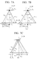
- Figs.6A to 6C and 7A to 7C show reasons why the aforementioned conditions 1) and 2) are satisfied, then the diffracted lights rll, r21 of the first and second wavelengths by the first diffraction area 29 are converged to much the same first position P1 on the light receiving element substrate 39, and the diffracted lights r12, r22 of the first and second wavelengths by the second diffraction area 31 are converged to substantially the same second position P2 on the light receiving element substrate 39.
- Fig.6A shows the + 1st order diffracted light rll and - 1st order diffracted light rll' diffracted by the first diffraction area 29 having the grating pitch ⁇ 1 and provided with the first wavelength.
- Fig.6B shows the + 1st order diffracted light r21 and - 1st order diffracted light r21' diffracted by the first diffraction area 29 and provided with the second wavelength.
- the grating pitch ⁇ 1 is set to satisfy the aforementioned condition 1). Therefore, when the distance L11 between an incident position P11 of the + 1st order diffracted light r11 of the first wavelength ⁇ 1 to the surface of the light receiving element substrate 39 and the optical axis A1 determined by the 0th order transmitted light of the first wavelength ⁇ 1 by the first diffraction area 29 is the first distance, and the distance L21 between an incident position P21 of the + 1st order diffracted light r21 of the second wavelength ⁇ 2 to the surface of the light receiving element substrate 39 and the optical axis A2 determined by the 0th order transmitted light of the second wavelength ⁇ 2 by the same diffraction area is the second distance, the difference
- Figs.7A to 7C show not only that the diffracted lights r11, r21 are converged to much the same first position P1, but also that the diffracted lights r12, r22 by the second diffraction area 31 are also converged to substantially the same second position P2 on the light receiving element substrate 39.
- Fig.7A shows the + 1st order diffracted lights r11, r11' of the first wavelength by the first diffraction area 29 having the grating pitch ⁇ 1, and the + 1st order diffracted lights r12, r12' of the first wavelength ⁇ 1 by the second diffraction area 31 having the grating pitch ⁇ 2.
- Fig.7B shows the ⁇ 1st order diffracted lights r21, r21' of the second wavelength by the first diffraction area 29 and the ⁇ 1st order diffracted lights r22, r22' of the second wavelength by the second diffraction area 31.
- the grating pitches ⁇ 1, ⁇ 2 are set to satisfy the aforementioned condition 1). Therefore, when distances L11, L12 between the incident positions P11, P12 of the + 1st order diffracted lights r11, r12 of the first wavelength ⁇ 1 to the light receiving element substrate 39 surface by the first diffraction area 29 and second diffraction area 31 and the optical axis A1 determined by the 0th order transmitted light of the first wavelength ⁇ 1 are first distances, and distances L21, L22 between the incident positions P21, P22 of the diffracted lights r21, r22 of the second wavelength ⁇ 2 to the light receiving element substrate 39 surface by the same diffraction area and the optical axis A2 determined by the 0th order transmitted light of the first wavelength ⁇ 2 are second distances, differences
- P11 becomes substantially equal to P21
- P12 becomes substantially equal to P22.
- the diffracted lights r11, r21 of the first and second wavelengths by the first diffraction area 29 are converged to much the same first position P1 on the light receiving element substrate 39
- the diffracted lights r12, r22 of the first and second wavelengths by the second diffraction area 31 are converged to substantially the same second position P2 on the light receiving element substrate 39.
- the interval S1 between the incident positions P11 and P12 of the + 1st order diffracted lights r11 and r12 shown in Fig.7A does not strictly or necessarily agree with the interval S2 between the incident positions P21 and P22 of the + 1st order diffracted lights r21 and r22 shown in Fig.7B and provided with the second wavelength ⁇ 2.
- the interval d between the first light source 25 and the second light source 27, and the grating pitches ⁇ 1, ⁇ 2 of the first diffraction area 29 and second diffraction area 31 have to be determined in such a manner that P11 and P21, or P12 and P22 agree with each other in the error range of a size of the first or second light receiving element 35, 37.
- Figs.8 and 9 show a method of determining the grating pitches ⁇ 1, ⁇ 2 and the interval d between the first and second light sources 25, 27.
- step S1 the interval h between the light receiving element substrate 39 and the holographic optical element 33 is determined.
- the interval L11 between the optical axis A1 and the incident position P11 of the diffracted light rll is determined. Furthermore, a diffraction angle ⁇ 11 of the diffracted light r11 is determined based on these values h and L11.
- step S2 based on the diffraction angle ⁇ 11 obtained in the step S1 and the value of the first wavelength ⁇ 1, the grating pitch ⁇ 1 is determined by diffraction formula.
- step S3 based on the grating pitch ⁇ 1 of the first diffraction area 29 and the value of the second wavelength ⁇ 2, a diffraction angle 021 of the diffracted light r21 is determined.
- step S4 based on the diffraction angle ⁇ 21 obtained in the step S3 and the interval h , the incident position P21 of the diffracted light r21, and the interval L21 between the position P21 and the optical axis A2 are determined.
- step S5 the grating pitch ⁇ 2 is determined in such a manner that a diffraction angle ⁇ 12 of the diffracted light r12 becomes equal to the diffraction angle ⁇ 21 of the diffracted light r21.
- step S6 based on the grating pitch ⁇ 2 and the value of the second wavelength ⁇ 2, by the diffraction formula, a diffraction angle ⁇ 22 of the diffracted light r22 is determined. Moreover, from the diffraction angle ⁇ 22, the incident position P22 of the diffracted light r22, and the interval L22 between the position P22 and the optical axis A2 are determined.
- the grating pitches ⁇ 1, ⁇ 2 and the interval d between the first and second light sources 25, 27 determined by the aforementioned method are as follows. For example, when the interval h between the light receiving element substrate 39 and the holographic optical element 33 is 3000 ⁇ m, and the interval L11 is 500 ⁇ m, the grating pitch ⁇ 1 of the first diffraction area 29 is determined as about 4.0 ⁇ m, the grating pitch ⁇ 2 of the second diffraction area 31 is determined as about 3.3 ⁇ m, and the interval d between the light emitting points of the light sources is determined as about 120 ⁇ m.
- the interval between the incident positions P11 and P21 is about 11 ⁇ m, and the interval between the incident positions P21 and P22 is about 12 ⁇ m.
- intervals s4, s5, s6 of incident points P11', P12', P21', P22' of the - 1st order diffracted lights r11', r12', r21', r22' to the light receiving element substrate 39 are about 104 ⁇ m, 120 ⁇ m, 130 ⁇ m, respectively.
- the grating pitches ⁇ 1, ⁇ 2 and the interval d between the first and second light sources 25, 27 are determined in such a manner that the + 1st order diffracted lights r11, r21 by the first diffraction area 29 are both converged to substantially the same position on the light receiving element substrate 39 in the error range of about 10 ⁇ m, and the + 1st order diffracted lights r12, r22 are also converged to substantially the same position on the light receiving element substrate 39 in the error range of about 10 ⁇ m.
- Figs.10 to 12 show a second embodiment of the optical device of the present invention.
- the first and second light receiving elements 35, 37 are positioned on both sides of an axis w connecting the optical axis A1 to A2 in substantially the same position in the X axis direction.
- the third to sixth light receiving elements 43 to 49 and ninth and tenth light receiving elements 55, 57 are disposed.
- the third and fourth light receiving elements 43, 45 receive the - 1st order diffracted lights rll', r12' having the first wavelength from diffraction areas 129, 131.
- the fifth and sixth light receiving elements 47, 49 receive the - 1st order diffracted lights r21', r22' having the second wavelength from the diffraction areas 129, 131.
- the ninth and tenth light receiving elements 55, 57 receive three beams for CD.
- Y axis direction dimensions of these elements 55, 57 are determined (e.g., about 90 ⁇ m) in such a manner that an incident luminous flux diameter (e.g., about 80 ⁇ m) is covered, and inclination angles are determined in such a manner that the elements fail to overlap with each other in the vicinity of the X axis.
- the third and fourth light receiving elements 43, 45 are apart from each other by the predetermined distance in the Y axis direction in substantially the same position in the X axis direction, and disposed on both sides of the axis w .
- the fifth and sixth light receiving elements 47, 49 are also apart from each other by the predetermined distance in the Y axis direction in substantially the same position in the X axis direction, and disposed on both sides of the axis w .
- the interval between the fifth and sixth light receiving elements 47, 49 is larger than the interval between the third and fourth light receiving elements 43, 45.
- the ninth and tenth light receiving elements 55, 57 are disposed on both sides of the fifth and sixth light receiving elements 47, 49, respectively. Specifically, the ninth and tenth light receiving elements 55, 57 are aligned with the light receiving elements 47, 49 in the Y axis direction.
- the light receiving elements 43, 45, and 47, 49 are disposed apart from each other in the X axis direction, and the interval is, for example, about 210 ⁇ m.
- the second embodiment of the optical device has the following constitution.
- the optical device is provided with the first light source 25 for outputting the light of the first wavelength ⁇ 1, and the second light source 27 for outputting the light of the second wavelength ⁇ 2.
- the first wavelength ⁇ 1 is, for example, 650 nm for a DVD
- the second wavelength ⁇ 2 is, for example, 780 nm for a CD.
- the interval d between the light emitting points of the light sources 25, 27 is set, for example, to about 104 ⁇ m.
- directions of grating axes u, v of the respective diffraction areas 129, 131 have angles ⁇ , ⁇ with respect to the Y axis.
- the angles ⁇ , ⁇ are set, for example, to a value of the order of 8.6 degrees.
- the grating axes u, v of the diffraction areas 129, 131 have an angle of about 17.2 degrees with each other.
- the grating pitches ⁇ of the first and second diffraction areas 129 and 131 of the holographic optical element 133 are both set to about 4.0 ⁇ m.
- the interval between the light receiving element substrate 39 and the holographic optical element 133 is set, for example, to 3000 ⁇ m similarly as the first embodiment.
- the DVD luminous flux emitted from the first light source 25 and provided with the first wavelength is reflected by the information recording medium (not shown), and subsequently diffracted by the first diffraction area 129 and second diffraction area 131 to produce + 1st order diffracted lights r11, r12, r11' , r12'.
- the + 1st order diffracted light rll by the first diffraction area 129 is converged to the first light receiving element 35
- the + 1st order diffracted light r12 by the second diffraction area 131 is converged to the second light receiving element 37.
- the - 1st order diffracted lights r11', r12' by the first diffraction area 129 and second diffraction area 131 are converged to the third light receiving element 43 and fourth light receiving element 45, respectively.
- the CD luminous flux provided with the second wavelength from the second light source 27 is reflected by the information recording medium (not shown), then diffracted by the first and second diffraction areas 129, 131 to produce the + 1st order diffracted lights r21, r22, r21', r22'. Subsequently, the + 1st order diffracted light r21 by the first diffraction area 129 is converged to the first light receiving element 35, and the + 1st order diffracted light r22 by the second diffraction area 131 is converged to the second light receiving element 37.
- the - 1st order diffracted lights r21', r22' by the first diffraction area 129 and second diffraction area 131 are converged to the fifth light receiving element 47 and sixth light receiving element 49, respectively.
- the concave lens action is applied to the diffracted lights r11, r21, and the convex lens action is applied to the diffracted lights r12, r22. Therefore, similarly as the first embodiment, the focus error signal by the complementary spot size method can be obtained on the basis of the outputs from the first light receiving element 35 and second light receiving element 37.
- the tracking error signal of the DVD luminous flux having the first wavelength can be obtained.
- the tracking error signal of the CD-R luminous flux having the second wavelength can be obtained.
- the 3-beam generating diffraction grating (not shown) is disposed between the second light source 27 and the information recording medium.
- the 3-beam generating diffraction grating (not shown) is formed, for example, on the surface opposite to the surface provided with the holographic optical element 133 in the diffraction element substrate (not shown) provided with the holographic optical element 133.
- the ninth and tenth light receiving elements 55, 57 are disposed on both sides of the fifth and sixth light receiving elements 47, 49, respectively.
- the CD luminous flux emitted from the second light source 27 is branched to three luminous fluxes aligned in a tangential direction (Y axis direction) of the information recording medium by the 3-beam generating diffraction grating (not shown).
- the three luminous fluxes are reflected by the information recording medium 21, then diffracted by the first and second diffraction areas 129, 131, diffracted with the same diffraction angle as that of the diffracted lights r21', r22', and converged onto the light receiving elements 55, 47, 57 or the light receiving elements 55, 49, 57 aligned in the Y axis direction on the light receiving element substrate 39. Therefore, for example, based on the outputs from the light receiving elements 55, 57, the tracking error signal of the CD luminous flux by the 3-beam method can be obtained.
- Figs.13A and 13B show the detailed constitution of the first to sixth light receiving elements 35, 37, 43, 45, 47, 49 and the ninth and tenth light receiving elements 55, 57. More specifically, Fig.13A shows a case in which the DVD luminous flux is incident upon the light receiving element, and a hatch mark 201 represents the spot of the DVD luminous flux on the light receiving element. Moreover, Fig.13B shows a case in which the CD luminous flux is incident upon the light receiving element, and a hatch mark 203 represents the spot of the CD luminous flux on the light receiving element.
- the first light receiving element 35 and second light receiving element 37 are divided into three light receiving areas 35a, 35b, 35c and light receiving areas 37a, 37b, 37c substantially along the Y axis direction.
- the third, fourth, fifth, sixth light receiving elements 43, 45, 47, 49 are divided into two light receiving areas 43a, 43b; 45a, 45b; 47a, 47b; 49a, 49b substantially along the Y axis direction, respectively.
- the focus error signals of the DVD luminous flux of the first wavelength ⁇ 1 and the CD luminous flux of the second wavelength ⁇ 2 can be obtained.
- the tracking error signal of the DVD luminous flux is, similarly as the first embodiment, given by outputs D1, D3 from the light receiving areas 43a, 43b of the third light receiving element 43 and outputs D2, D4 from the light receiving areas 45a, 45b of the fourth light receiving element 45.
- the second embodiment is provided with the following advantages.
- the arrangement positions of the first and second light sources 25, 27, the grating axis directions u, v of the first and second diffraction areas 129, 131, and the positions of the first and second light receiving elements 35, 37 are determined, for example, as follows.
- a virtual diffraction grating provided with the same grating pitch as that of the first and second diffraction areas and directed in an arbitrary direction
- a circle drawn by a resulting virtual diffracted light on the light receiving element substrate 39 (hereinafter referred to the diffraction circle) is q1.
- the diffraction circle drawn by the resulting virtual diffracted light on the light receiving element substrate 39 is q2.
- the interval d between the optical axes A1 and A2 is determined in such a manner that the diffraction circle ql contacts the diffraction circle q2.
- the positions P1, P2 in the vicinity of a point at which the diffraction circles ql and q2 contact each other are the arrangement positions of the first light receiving element 35 and second light receiving element 37.
- the positions P1, P2 of the light receiving elements 35, 37 may be any positions as long as the interval between the diffraction circles q1 and q2 is 50 ⁇ m or less (preferably, 20 ⁇ m or less).
- the grating axis directions u, v of the first and second diffraction areas 129, 131 are determined in such a manner that the diffracted lights r11, r21, r12, r22 of the first and second wavelengths by the diffraction areas 129, 131 are converged onto the light receiving elements 35, 37.
- the complementary focus error detection can be realized by a 2-wavelength optical system with respect to the two wavelengths. Therefore, in a DVD and CD-R compatible pickup or a reproduction apparatus, miniaturization, simplification, cost reduction, and high efficiency can be realized.
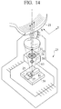
- Figs,14 to 16 show a third embodiment of the optical device of the present invention.
- the first laser light source 25 for generating a DVD laser light 1d
- the second laser light source 27 for generating a CD laser light 1c.
- the light emitting points of the first and second light sources 25, 27 are apart from each other by the predetermined distance d in the X axis direction as the radial direction of the recording medium 21.
- the interval d is, for example, about 104 ⁇ m.
- the light receiving element substrate 39 is also provided with a reflection mirror 61 for reflecting the DVD laser light 1d and CD laser light 1c from the first laser light source 25 and second laser light source 27 toward the recording medium 21.
- a 3-beam generating diffraction grating 28 for branching beams 1d, 1c from the reflection mirror 61 into a main beam B0, and side beams B1, B2, and the holographic optical element 33 for directing the reflected beam from the recording medium 21 to the light receiving element substrate 39 are disposed on lower and upper surfaces of a diffraction element substrate 63 disposed between the reflection mirror 61 and the recording medium 21.
- the grating pitch of the 3-beam generating diffraction grating 28 and the grating pitch and grating arrangement angle of the first and second areas 29, 31 of the holographic optical element are set as follows.
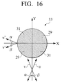
- the holographic optical element first and second areas 29 and 31 are constituted by the diffraction areas provided with the grating axes whose directions u, v form angles ⁇ , ⁇ with respect to the Y axis as a track tangential direction of the recording medium 21.
- the areas are formed in such a manner that a diffraction axis direction u' of the ⁇ 1st order diffracted light by the first area 29, and a diffraction axis direction v' of the ⁇ 1st order diffracted light by the second area 31 form the predetermined angles ⁇ , ⁇ in opposite directions with respect to a radial axis X crossing at right angles of the track of the information recording medium 21.
- the grating pitches of the areas 29, 31 are the same and the angle ⁇ is equal to ⁇ .
- the grating pitch of the holographic optical element first area 29 is determined in such a manner that substantially the same position P1 on the light receiving element substrate 39 (Fig.15) is irradiated with + 1st order diffracted lights rd1, rc1 (Fig.15) of the main beam B0 of the DVD laser light 1d and CD laser light 1c by the area 29.
- the grating pitch of the holographic optical element second area 31 is determined in such a manner that substantially the same position P2 on the light receiving element substrate 39 (Fig.15) is irradiated with + 1st order diffracted lights rd2, rc2 of the main beam B0 of the DVD laser light 1d and CD laser light 1c by the area 31.
- the + 1st order diffracted light of the beam B0 by the first area 29 is rd1
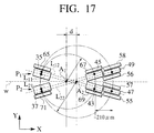
- the distance L11 between the incident position P1 of the diffracted light rd1 onto the light receiving element substrate 39 and the optical axis A1 determined by the 0th order transmitted light is the first distance (Fig.17).
- the + 1st order diffracted light of the beam B0 by the first diffraction area 29 is rcl
- the distance L12 between the incident position P1 of the diffracted light rc1 onto the light receiving element substrate 39 and the optical axis A2 determined by the 0th order transmitted light is the second distance.
- between the distances L11 and L12 is determined to be equal to the interval d between the light emitting points of the light sources 25, 27.
- the grating pitch is set, for example, to about 4.0 ⁇ m.
- angles of the grating axes u, v of the first and second areas 29, 31 are determined in such a manner that the + 1st order diffracted light of the beam B0 of the DVD and CD laser lights by the second area 31 is converged substantially to the second position P2 apart from the first position P1 on the light receiving element substrate 39 in the Y axis direction by a sufficient distance for disposing the light receiving elements 35, 37.
- This angle ⁇ ⁇ is set, for example, to about 8.6°.
- the position P1 is irradiated with the + 1st order diffracted light of the main beam B0 by the first area 29 on the light receiving element substrate 39.
- the position P2 is irradiated with the + 1st order diffracted light of the main beam B0 by the second area 31 on the light receiving element substrate 39, with respect to both the DVD laser light and the CD laser light (see Figs.15 and 17).
- the grating pitch of the 3-beam generating diffraction grating 28 is determined in accordance with an open angle of the hologram grating axes u, v as follows.
- the + 1st order diffracted light of the second side beam B2 by the hologram first area 29 is determined to be overlapped with the + 1st order diffracted light of the first side beam B1 by the second area 31 on the light receiving element substrate.
- the - 1st order diffracted light of the first side beam B1 by the hologram first area 29 is overlapped with the - 1st order diffracted light of the second side beam B2 by the second area 31.
- the first light receiving element 35 for receiving the + 1st order diffracted lights rdl, rcl of the main beam in the DVD laser light (hereinafter referred to as the DVD main beam) and the main beam in the CD laser light (hereinafter referred to as the CD main beam) by the first area 29.
- the second light receiving element 37 for receiving the + 1st order diffracted lights rd2, rc2 of the DVD main beam and the CD main beam by the second area 31.
- the third and fourth light receiving elements 43 and 45 for receiving the - 1st order diffracted lights rd1' and rd2' of the DVD main beam B0 by the first and second areas 29 and 31 are disposed on the light receiving element substrate 39.
- the fifth and sixth light receiving elements 47 and 49 for receiving the - 1st order diffracted lights rc1' and rc2' of the CD main beam B0 by the first and second areas 29 and 31 are disposed.
- the first and second light receiving elements 35 and 37 are divided into three areas 35a, 35b, 35c, and 37a, 37b, 37c aligned in the Y axis direction, respectively.
- the third, fourth, fifth, sixth light receiving elements 43, 45, 47, 49 are provided with two light receiving areas 43a and 43b, 45a and 45b, 47a and 47b, and 49a and 49b aligned in the Y axis direction, respectively.
- the eight and seventh light receiving elements 57 and 55 are disposed on both sides of the fifth light receiving element 47 (aligned position in the Y axis direction). Furthermore, to receive the - 1st order diffracted light of the CD side beams B1 and B2 by the second area 31, the tenth and ninth light receiving elements 58 and 56 are disposed on both sides of the sixth light receiving element 49.
- an eleventh light receiving element 65 is disposed outside the first light receiving element 35 (on the side apart from the axis w in the Y axis direction), and to receive the - 1st order diffracted light of the DVD side beam B1 by the second area 31, a twelfth light receiving element 67 is disposed outside the fourth light receiving element 45 (additionally, the axis w is an axis on the light receiving element substrate, which connects the axes A1 and A2 determined by the 0th order transmitted lights of the DVD and CD main beams as shown in the drawing).
- a thirteenth light receiving element 69 is disposed outside the third light receiving element 43 to receive the - 1st order diffracted light of the DVD side beam B2 by the first area 29.
- a fourteenth light receiving element 71 is disposed outside the second light receiving element 37 to receive the + 1st order diffracted light of the DVD side beam B2 by the second area 31.
- the eleventh, twelfth, thirteenth, fourteenth light receiving elements 65, 67, 69, 71 are divided into two light receiving areas 65a and 65b, 67a and 67b, 69a and 69b, and 71a and 71b aligned in the Y axis direction, respectively.
- Fig.18 shows a state in which the diffracted light of the CD laser light is incident upon the respective light receiving elements in the optical device 23.
- the + 1st order diffracted light of the main beam B0 by the first area 29 is incident upon the first light receiving element 35 to form a double fan-shaped spot 75, and the - 1st order diffracted light is incident upon the fifth light receiving element 47 to form a double fan-shaped spot 79.
- the shapes of the double fan-shaped spots 75, 79 are analogous to the shape of the hologram first area 29.
- the + 1st order diffracted light of the main beam B0 by the second area 31 is incident upon the second light receiving element 37 to form a double fan-shaped spot 77 and the - 1st order diffracted light is incident upon the sixth light receiving element 49 to form a double fan-shaped spot 85.
- the - 1st order diffracted light of the first side beam B1 by the hologram first area 29 is incident upon the ninth light receiving element 57 to form a double fan-shaped spot 83.
- the - 1st order diffracted light of the first side beam B1 by the hologram second area 31 is incident upon the tenth light receiving element 58 to form a double fan-shaped spot 89.
- the - 1st order diffracted light of the second side beam B2 by the hologram first area 29 is incident upon the seventh light receiving element 55 to form a double fan-shaped spot 81.
- the - 1st order diffracted light of the second side beam B2 by the hologram second area 31 is incident upon the eighth light receiving element 56 to form a double fan-shaped spot 87.
- the lens power is applied in such a manner that the area acts on the diffracted light rc1 as convex lens, and acts on the diffracted light rc2 as the concave lens.
- the convex lens power is applied to the diffracted light for generating the spot 75
- the concave lens power is applied to the diffracted light for generating the spot 77.
- the recording signal RF is detected as the sum of outputs from the light receiving elements 35, 37, 47, 49.
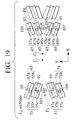
- Fig.19 shows a state in which the diffracted light of the DVD laser light is incident upon the respective light receiving elements in the optical device 23.
- the + 1st order diffracted light of the main beam B0 by the first area 29 is incident upon the light receiving element 35 to form a double fan-shaped spot 91, and the - 1st order diffracted light is incident upon the third light receiving element 43 to form a double fan-shaped spot 95.
- the + 1st order diffracted light of the main beam B0 by the second area 31 is incident upon the second light receiving element 37 to form a double fan-shaped spot 93 and the - 1st order diffracted light is incident upon the fourth light receiving element 45 to form a double fan-shaped spot 97.
- the + 1st order diffracted light of the first side beam B1 by the hologram first area 29 is incident upon the light receiving element 65 to form a double fan-shaped spot 99, and the - 1st order diffracted light is incident upon a middle point P4 between the light receiving elements 43 and 45 to form a spot 101.
- the + 1st order diffracted light of the first side beam B1 by the hologram second area 31 is incident upon a middle point P3 between the light receiving elements 35 and 37 to form a spot 103, and the - 1st order diffracted light forms a double fan-shaped spot 105 in the light receiving element 67.
- the + 1st order diffracted light of the second side beam B2 by the hologram first area 29 is superposed upon the spot 103 in the middle point P3 between the light receiving elements 35 and 37, and the - 1st order diffracted light is incident upon the thirteenth light receiving element 69 to form a double fan-shaped spot 107.
- the + 1st order diffracted light of the second side beam B2 by the hologram second area 31 is incident upon the fourteenth light receiving element 71 to form a double fan-shaped spot 109, and the - 1st order diffracted light is superposed upon the spot 101 in the middle point P4 between the light receiving elements 43 and 45.
- the convex lens power is applied to the + 1st order diffracted light for generating the spot 91
- the tracking error signal of the 3-beam DPP method can be detected.
- detection is as follows.
- the tracking error signal of the 3-beam DPP method is detected as follows.
- a tracking error signal TEdpp of the three beam DPP system is given by the following equation.
- TEdpp [(A0 + D0) - (B0 + C0)]-k[(A1 + D1 + A2 + D2) - (B1 + C1 + B2 + C2)]
- k denotes a constant determined in accordance with the standard of the disc or the like, and has a size of the order of 1 to 10.
- Fig.21 is an explanatory view showing a relation between the double fan-shaped spots of the diffracted lights incident upon the light receiving elements 43, 45, 65, 67, 69, 71 and the light receiving areas of the light receiving elements.
- the double fan-shaped spot 95 on the third light receiving element 43 has a strength proportional to the light strengths A0, C0 in the first area
- the spot 97 on the light receiving element 45 has a strength proportional to the light strengths B0, D0 in the second area 31.
- a right upper fan portion of the spot 95 having the strength A0 is incident upon a light receiving area 43a
- a left lower fan portion having the strength C0 is incident upon a light receiving area 43b.
- a right lower fan portion of the spot 97 having the strength B0 is incident upon a light receiving area 45b
- a left upper fan portion having the strength D0 is incident upon a light receiving area 45a in the constitution.
- a right-side light strength of the main beam B0 in the incident position upon the holographic optical element 33 can be detected.
- a left-side light strength of the main beam B0 in the incident position upon the holographic optical element 33 can be detected.
- the right-side light intensity during incidence of the first side beam on the holographic optical element is detected as the sum of outputs from the light receiving areas 65b, 67a
- the left-side light intensity is detected as the sum of outputs from the light receiving areas 65a, 67b.
- the right-side light intensity during input of the second side beam to the holographic optical element is detected as the sum of outputs from the light receiving areas 69a, 71b
- the left-side light intensity is detected as the sum of outputs from the light receiving areas 71a, 69b.
- the constant k is the same as the constant k in the equation (2).
- the recording signal RF is detected as the sum of outputs from the light receiving elements 35, 37, 43, 45.
- Fig.22 shows one example of an electric circuit for obtaining the tracking error signal TEdpp of DPP system based on the outputs from the light receiving areas 43a, 43b, 45a, 45b, 65a, 65b, 67a, 67b, 69a, 69b, 71a, 71b.
- boundary lines and division lines of the light receiving areas 43a, 43b, 45a, 45b, 65a, 65b, 67a, 67b, 69a, 69b, 71a, 71b are disposed in parallel to the X axis. Therefore, even when the holographic optical element spot shifts in the X axis direction by wavelength fluctuation, the spot only moves along the boundary line or the division line of the light receiving area. Therefore, error generation by the wavelength fluctuation of the detection laser light can be avoided.
- the tracking error detection of the 3-beam DPP system for a DVD-RAM is possible, and the influence of lens shift or the like can be minimized.
- the light receiving area and division line are set in a direction inactive to the wavelength fluctuation, but in this case, several degrees of deviations are generated from the diffraction light movement direction (radial axis direction) by objective lens movement.
- the objective lens position largely changes, focus error signal detecting sensitivity deterioration, offset generation, jitter, and error rate deterioration are caused.
- the direction of the light receiving area and division line is determined to be different from the diffraction direction and radial axis direction and to indicate the predetermined angle in the middle of both directions.
- the optical device is provided with the first light source 25 for outputting the light of the first wavelength ⁇ 1, and the second light source 27 for outputting the light of the second wavelength ⁇ 2.
- the first wavelength ⁇ 1 is, for example, 650 nm for a DVD
- the second wavelength ⁇ 2 is, for example, 780 nm for a CD.
- the interval d between the light emitting points of the light source 25, 27 is set, for example, to about 104 ⁇ m.
- the interval between the light receiving element substrate 39 and the holographic optical element 133 is set, for example, to 3000 ⁇ m.
- the DVD luminous flux emitted from the first light source 25 and provided with the first wavelength is reflected by the information recording medium (not shown), and subsequently diffracted by the first diffraction area 129 and second diffraction area 131 to produce the ⁇ 1st order diffracted lights r11, r12, r11', r12'.
- the + 1st order diffracted light r11 by the first diffraction area 129 is converged to a first light receiving element 35a
- the + 1st order diffracted light r12 by the second diffraction area 131 is converged to a second light receiving element 37a.
- the - 1st order diffracted lights r11', r12' by the first diffraction area 129 and second diffraction area 131 are converged to the third light receiving element 43a and fourth light receiving element 45a, respectively.
- the CD luminous flux provided with the second wavelength from the second light source 27 is reflected by the information recording medium (not shown), then diffracted by the first and second diffraction areas 129, 131 to produce the ⁇ 1st order diffracted lights r21, r22, r21', r22'. Subsequently, the + 1st order diffracted light r21 by the first diffraction area 129 is converged to the first light receiving element 35a, and the + 1st order diffracted light r22 by the second diffraction area 131 is converged to the second light receiving element 37a.
- the - 1st order diffracted lights r21', r22' by the first diffraction area 129 and second diffraction area 131 are converged to a fifth light receiving element 47a and a sixth light receiving element 49a, respectively.
- the concave lens action is applied to the diffracted lights r11, r21, and the convex lens action is applied to the diffracted lights r12, r22. Therefore, similarly as the second embodiment, the focus error signal by the complementary spot size method can be obtained on the basis of the outputs from the first light receiving element 35a and second light receiving element 37a.
- the tracking error signal of the DVD luminous flux having the first wavelength can be obtained.
- the tracking error signal of the CD-R luminous flux having the second wavelength can be obtained.
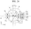
- Fig.25A is an explanatory view showing the relation between the spot of the diffracted light incident upon the light receiving element and the light receiving area of the light receiving element
- Fig.25B is a partial enlarged view.
- each of the light receiving elements 35a, 37a, 43a, 45a allows spot position movement centering on and including a standard spot position and caused by the respective error factors, a rectangular shape long in one direction with respect to spots 8a+, 8a-, 8b+, 8b- is formed.
- the light receiving area is further divided into a plurality of sub areas 16 by a division line 14, but this division line 14 is set to be substantially parallel to a side of a longitudinal direction 12 in the rectangular light receiving area.
- An inclination angle ⁇ 2 of the longitudinal direction side of the rectangle and the dividing line 14 to the radial axis is determined to satisfy the following relation with respect to an angle ⁇ 1 of diffraction directions 10a, 10b to the radial axis: 0 ⁇ ⁇ 2 ⁇ ⁇ 1 .
- a direction 12a of each light receiving element and division line 14 is disposed between a radial axis direction W and a diffraction direction 10a.
- the spot position slightly fluctuates with respect to the division line 14, but it is apparent that the fluctuation is smaller than that of the second embodiment (the diffraction direction agrees with the longitudinal direction of the light receiving element).
- the spot position slightly fluctuates with respect to the division line 14, but it is apparent that the fluctuation is smaller than that of the second embodiment.
- the fourth embodiment in the integrated pickup which is applied to high-density discs such as a DVD and the small size, high speed and low cost can be satisfied, even when the diffraction direction of hologram or the like disagrees with the radial axis direction, with respect to a plurality of error factors such as wavelength fluctuation, diffraction element position error, relative position error of the light emitting element and light receiving element, and diffracted light movement caused by the tracking operation, the allowance distribution is performed without any dispersion, the total allowance for each element dispersion and assembly can be satisfied, every error factor is provided with a certain degree of allowance, and the balanced and highly practical optical device can be realized.
- error factors such as wavelength fluctuation, diffraction element position error, relative position error of the light emitting element and light receiving element, and diffracted light movement caused by the tracking operation
Landscapes
- Physics & Mathematics (AREA)
- Optics & Photonics (AREA)
- Optical Head (AREA)
- Optical Recording Or Reproduction (AREA)
Abstract
Description
FE = S1 - S2.
RF = S1 + S2 + D1 + D2 + D3 + D4.
FE = S1 - S2.
TE = E - F.
RF = S1 + S2 + R1 + R2.
TE(pp/CD-R) = R1 - R2.
FE = S1 - S2.
TE = E - F.
TE(pp/CD-R) = R1 - R2.
RF = S1 + S2 + D1 + D2 + D3 + D4.
RF = S1 + S2 + R1 + R2.
FE = S1 - S2.
TE = E - F.
FE = S1 - S2.
0 < 2 < 1.
(ΔL + Δh)sin(1 - 2) = (Δx + Δr)sin2; or
(k1ΔL + k2Δh)sin(1 - 2) = (k2Δx + Δr)sin2, where 0 < k1 <1 and 0< k2 < 1.
Claims (14)
- An optical device for reading information from an information recording medium (21), comprising:a first light source (25) for outputting a light of a first wavelength (λ1);a second light source (27) for outputting a light of a second wavelength (λ2);a holographic optical element (33) having a first diffraction area (29) and a second diffraction area (31) for diffracting the lights of said first and second wavelengths; anda light receiving element substrate (39) provided with a first light receiving element (35) and a second light receiving element (37) for receiving a diffracted light from said holographic optical element (33), wherein
said first diffraction area (29) and the second diffraction area (31) have grating arrangements whose grating axis directions are parallel to each other and whose grating pitches (Λ1, Λ2) are different from each other, and light emitting points of said first and second light sources (25, 27) are apart from each other by a predetermined distance (d) in a direction crossing at right angles to said grating axis,the grating pitches (Λ1, Λ2) of said first diffraction area (29) and the second diffraction area (31) are determined in such a manner that:when a distance (L11; L12) between an incident position (P1) of the diffracted light of said first wavelength to the surface of said light receiving element substrate by the first diffraction area or the second diffraction area, and an optical axis (A1) determined by a 0th order transmitted light of the first wavelength is a first distance, and a distance (L21; L22) between an incident position (P2) of the diffracted light of said second wavelength to said light receiving element substrate surface by the same diffraction area, and the optical axis (A2) determined by the 0th order transmitted light of the second wavelength is a second distance, a difference (|L11 - L21|; |L12 - L22|) between said first distance and the second distance becomes equal to an interval (d) between the light emitting points of said first and second light sources; andan interval (|L11 - L12|; |L21 - L22|) between the incident position (P1) of the diffracted light of said first or second wavelength to said light receiving element substrate surface by said first diffraction area, and the incident position (P1) of the diffracted light of the same wavelength to said light receiving element substrate surface by the second diffraction area becomes equal to the interval (d) between said light emitting points,the diffracted lights of the first wavelength and the second wavelength by said first diffraction area are converged to much the same first position (P1) on said light receiving element substrate, and the diffracted lights of the. first wavelength and the second wavelength by said second diffraction area are converged to about the same second position (P2) on said light receiving element substrate, andthe first and second light receiving elements (35, 37) are disposed in said first and second positions (P1, P2), respectively. - The optical device according to claim 1 wherein a focus error signal is obtained on the basis of signals from said first light receiving element (35) and the second light receiving element (37).
- The optical device according to claim 1 wherein the diffracted lights to said first and second positions (P1, P2) are both + 1st order diffracted lights by said first diffraction area (29) and the second diffraction area (31), and the interval (d) between the light emitting points of said first and second light sources (25, 27) and the grating pitches (Λ1, Λ2) of said first diffraction area and the second diffraction area are set in such a manner that - 1st order diffracted lights of said first wavelength and the second wavelength by said first diffraction area and the second diffraction area are converged to third, fourth, fifth, sixth positions (P3, P4, P5, P6) apart from one another by a predetermined interval capable of receiving the lights in independent light receiving areas not superposed to one another on said light receiving element substrate (39).
- The optical device according to claim 3 wherein the - 1st order diffracted lights of said first wavelength by said first diffraction area (29) and the second diffraction area (31) are converged to said third and fourth positions (P3, P4), the - 1st order diffracted lights of said second wavelength by said first diffraction area (29) and the second diffraction area (31) are converged to said fifth and sixth positions (P5, P6), a tracking error signal for the first wavelength (λ1) is obtained on the basis of detection signals from the light receiving elements (43, 45) disposed in said third and fourth positions (P3, P4), and a tracking error signal for the second wavelength (λ2) is obtained on the basis of the signals from the light receiving elements (47, 49) disposed in said fifth and sixth positions (P5, P6), or the signals from the light receiving elements (55, 57) disposed on both side areas opposite to each other in a grating axis direction of said fifth or sixth position.
- The optical device according to claim 4 wherein when said information recording medium (21) is a CD-R, the tracking error signal for said second wavelength (λ2) is obtained on the basis of the signals from the light receiving elements (47, 49) disposed in said fifth and sixth positions (P5, P6).
- An optical device for reading information from an information recording medium (21), comprising:a first light source (25) for outputting a light of a first wavelength (λ1);a second light source (27) for outputting a light of a second wavelength (λ2);a holographic optical element (133) having a first diffraction area (129) and a second diffraction area (131) for diffracting the lights of said first and second wavelengths; anda light receiving element substrate (39) provided with a first light receiving element (35) and a second light receiving element (37) for receiving a diffracted light from said holographic optical element (33), wherein
in said first diffraction area (129) and the second diffraction area (131), grating pitches (Λ) are identical with each other, grating axis directions are different from each other by a predetermined angle of 30° or less, and light emitting points of said first and second light sources (25, 27) are apart from each other by a predetermined distance (d) in a direction crossing at right angles to said grating axis direction,
the grating pitches (Λ) of said first diffraction area (129) and the second diffraction area (131) are determined in such a manner that:
when a distance between an incident position (P1) of the diffracted light of said first wavelength to the surface of said light receiving element substrate by the first diffraction area or the second diffraction area, and an optical axis (A1) determined by a 0th order transmitted light of the first wavelength is a first distance, and a distance between an incident position (P2) of the diffracted light of said second wavelength to the surface of said light receiving element substrate by the same diffraction area, and the optical axis (A2) determined by the 0th order transmitted light of the second wavelength is a second distance, a difference between said first distance and the second distance becomes equal to an interval (d) between the light emitting points of said first and second light sources,
directions of said first diffraction area (129) and the second diffraction area (131) are determined in such a manner that:
the diffracted lights of the first wavelength and the second wavelength by said first diffraction area are converged to much the same first position (P1) on said light receiving element substrate; and
the diffracted lights of the first wavelength and the second wavelength by said second diffraction area are converged to about the same second position (P2) apart from said first position by a predetermined distance in a direction crossing at right angles to the apart direction of said light emitting points on said light receiving element substrate, and
the first and second light receiving elements (35, 37) are disposed in said first and second positions (P1, P2), respectively. - The optical device according to claim 6 wherein a focus error signal is obtained on the basis of signals from said first light receiving element (35) and the second light receiving element (37).
- The optical device according to claim 6 wherein the diffracted lights to said first and second positions (P1, P2) are both + 1st order diffracted lights by said first diffraction area (29) and the second diffraction area (31), a tracking error signal of the light of said first wavelength (λ1) is obtained on the basis of signals from the light receiving elements (43, 45) disposed in the third and fourth positions in which the - 1st order diffracted lights of said first wavelength by said first diffraction area and the second diffraction area are converged on said light receiving element substrate, and a tracking error signal of the light of said second wavelength (λ2) is obtained on the basis of the signals from the light receiving elements (47, 49) disposed in the fifth and sixth positions in which the - 1st order diffracted light of said second wavelength by said first diffraction area or the second diffraction area is converged on said light receiving element substrate, or the signals from the light receiving elements (55, 57) disposed on both side areas opposite to each other in a grating axis direction of the fifth position or the sixth position.
- The optical device according to claim 8 wherein when said information recording medium (21) is a CD-R, the tracking error signal for said second wavelength (λ2) is obtained on the basis of the signals from the light receiving elements (47, 49) disposed in said fifth and sixth positions.
- The optical device according to claim 7 wherein said first light receiving element (35) and the second light receiving element (37) are divided into a plurality of sub areas (16) by a plurality of division lines (14), and the focus error signal is obtained on the basis of the signals from the plurality of sub areas (16).
- The optical device according to claim 10 wherein when a point at which said 0th order transmitted light intersects said light receiving element substrate is P, an angle formed by a radial axis defined in a radial direction crossing at right angles to a track of said information recording medium (21) and a straight line connecting said first or second position to said intersection point P is 1, and an angle formed by said radial axis and said plurality of division lines is 2, a relation of 0 < 2 < 1 is satisfied.
- An optical device for using a laser light having a predetermined wavelength (λ) to read information from an information recording medium (21), comprising:a laser light source (25) for generating said laser light;a light receiving element substrate (39) provided with a plurality of light receiving areas in the same plane;a 3-beam generating diffraction grating (28) for branching the laser light from said laser light source (25) to three emitted lights; anda holographic optical element (33), divided into at least a first area (29) and a second area (31) in the same plane, for branching a reflected light from said information recording medium (21) and turning the light to said light receiving element substrate (39),
wherein diffraction axes of said first area (29) and the second area (31) are formed in such a manner that a diffraction axis direction of ± 1st order diffracted lights by the first area and the diffraction axis direction of the ± 1st order diffracted lights by the second area form predetermined angles in opposite directions with respect to a radial axis crossing at right angles to a track of said information recording medium (21), and
said holographic optical element first area (29) and second area (31), and the 3-beam generating diffraction grating (28) are constituted in such a manner that
when one of the ± 1st order diffracted lights branched by said 3-beam generating diffraction grating is a first side beam (B1), and the other is a second side beam (B2),
the diffracted light of said first side beam (B1) by said first area (29) is overlapped with the diffracted light of said second side beam (B2) by said second area (31) on said light receiving element substrate (39). - The optical device according to claim 12 wherein a focus error signal is obtained on the basis of signals from a first light receiving element (35) and a second light receiving element (37) disposed in a first position in which the diffracted light diffracted by said first diffraction area (29) is converged on said light receiving element substrate and a second position in which the diffracted light diffracted by said second diffraction area (31) is converged on said light receiving element substrate, respectively.
- The optical device according to claim 12 wherein the diffracted lights to said first and second positions are both + 1st order diffracted lights by said first diffraction area ( 29) and the second diffraction area (33), and a tracking error signal is obtained on the basis of signals from the light receiving elements (43, 45) disposed in the third and fourth positions in which - 1st order diffracted lights by said first diffraction area (29) and the second diffraction area (31) are converged on said light receiving element substrate, and the signals from four light receiving elements (65, 67, 69, 71), disposed on said light receiving element substrate, for detecting the + 1st order diffracted light of said second side beam by said first area, the + 1st order diffracted light of said second side beam by said second area, the - 1st order diffracted light of said second side beam by said first area, and the - 1st order diffracted light of said second side beam by said second area, respectively.
Applications Claiming Priority (4)
| Application Number | Priority Date | Filing Date | Title |
|---|---|---|---|
| JP35806999 | 1999-12-16 | ||
| JP35806999A JP3518457B2 (en) | 1999-12-16 | 1999-12-16 | Optical device |
| JP2000312436A JP3536805B2 (en) | 2000-10-12 | 2000-10-12 | Optical pickup |
| JP2000312436 | 2000-10-12 |
Publications (3)
| Publication Number | Publication Date |
|---|---|
| EP1109163A2 true EP1109163A2 (en) | 2001-06-20 |
| EP1109163A3 EP1109163A3 (en) | 2003-07-09 |
| EP1109163B1 EP1109163B1 (en) | 2008-07-09 |
Family
ID=26580727
Family Applications (1)
| Application Number | Title | Priority Date | Filing Date |
|---|---|---|---|
| EP00127242A Expired - Lifetime EP1109163B1 (en) | 1999-12-16 | 2000-12-15 | Optical device |
Country Status (3)
| Country | Link |
|---|---|
| US (2) | US6512608B2 (en) |
| EP (1) | EP1109163B1 (en) |
| DE (1) | DE60039403D1 (en) |
Cited By (6)
| Publication number | Priority date | Publication date | Assignee | Title |
|---|---|---|---|---|
| WO2002091369A1 (en) * | 2001-05-03 | 2002-11-14 | Koninklijke Philips Electronics N.V. | Optical scanning device |
| GB2398926A (en) * | 2003-02-28 | 2004-09-01 | Richard Knight | Light emitting device |
| CN1297964C (en) * | 2002-09-10 | 2007-01-31 | 松下电器产业株式会社 | Optical pickup device |
| EP1630798A4 (en) * | 2003-01-30 | 2008-09-24 | Matsushita Electric Industrial Co Ltd | OPTICAL HEAD AND EQUIPMENT AND SYSTEM THEREFORE |
| US7830773B2 (en) | 2004-11-16 | 2010-11-09 | Panasonic Corporation | Optical pickup for recording and reproducing information with a plurality of types of optical information recording mediums |
| EP3046047A1 (en) * | 2015-01-16 | 2016-07-20 | Fujitsu Limited | Illumination apparatus and biometric authentication apparatus |
Families Citing this family (32)
| Publication number | Priority date | Publication date | Assignee | Title |
|---|---|---|---|---|
| JP2001256666A (en) * | 2000-03-09 | 2001-09-21 | Ricoh Co Ltd | Optical pickup device |
| JP2001256670A (en) * | 2000-03-10 | 2001-09-21 | Sony Corp | Optical pickup device and optical disk device |
| US7035196B2 (en) * | 2000-03-14 | 2006-04-25 | Matsushita Electric Industrial Co., Ltd. | Optical head device and optical recording and reproducing apparatus having lasers aligned in a tangential direction |
| US6928035B2 (en) * | 2000-07-07 | 2005-08-09 | Matsushita Electric Industrial Co., Ltd. | Optical pick-up, optical disk apparatus and information processing apparatus |
| KR100819625B1 (en) * | 2000-07-12 | 2008-04-04 | 소니 가부시끼 가이샤 | Optical pickup apparatus, optical disc apparatus, and track recognition signal detection method |
| US20020097660A1 (en) * | 2000-11-16 | 2002-07-25 | Matsushita Electric Industrial Co., Ltd. | Diffraction grating body, optical pick-up, semiconductor laser apparatus and optical information apparatus |
| JP2003281749A (en) * | 2002-03-25 | 2003-10-03 | Matsushita Electric Ind Co Ltd | Optical pickup |
| US7232650B2 (en) * | 2002-10-02 | 2007-06-19 | 3M Innovative Properties Company | Planar inorganic device |
| JP2004134032A (en) * | 2002-10-11 | 2004-04-30 | Funai Electric Co Ltd | Optical disk unit |
| KR100524986B1 (en) * | 2003-08-26 | 2005-10-31 | 삼성전자주식회사 | Optical pickup and optical recording and/or reproducing apparatus employing it |
| JP4177296B2 (en) * | 2004-06-22 | 2008-11-05 | シャープ株式会社 | Optical pickup and optical disk apparatus |
| JP2006099859A (en) * | 2004-09-29 | 2006-04-13 | Matsushita Electric Ind Co Ltd | Optical pickup device |
| JP4277005B2 (en) * | 2005-01-26 | 2009-06-10 | パナソニック株式会社 | Optical pickup device |
| JP2006268974A (en) * | 2005-03-24 | 2006-10-05 | Matsushita Electric Ind Co Ltd | Optical semiconductor device |
| JP4229924B2 (en) * | 2005-04-25 | 2009-02-25 | パナソニック株式会社 | Optical pickup device |
| JP2007134016A (en) * | 2005-11-14 | 2007-05-31 | Funai Electric Co Ltd | Optical pickup device |
| KR101428956B1 (en) * | 2006-04-12 | 2014-08-12 | 도요세이칸 그룹 홀딩스 가부시키가이샤 | Structure, forming method of structure, structure forming device, structure color and/or diffraction light reading method, and truth/false discriminating method |
| JP2008146741A (en) * | 2006-12-08 | 2008-06-26 | Matsushita Electric Ind Co Ltd | Optical pickup device |
| US20080165655A1 (en) * | 2007-01-09 | 2008-07-10 | Ryo Saitoh | Optical pickup device |
| US7635836B2 (en) * | 2007-02-21 | 2009-12-22 | Intersil Americas Inc. | Configurable photo detector circuit |
| US7663087B2 (en) * | 2007-02-27 | 2010-02-16 | Intersil Americas Inc. | Dynamically configurable multiple wavelength photodetector array for optical storage applications |
| JP4552956B2 (en) * | 2007-04-03 | 2010-09-29 | セイコーエプソン株式会社 | Lighting device and projector |
| JP2010009682A (en) * | 2008-06-27 | 2010-01-14 | Panasonic Corp | Optical head device, optical information processing device, and signal detection method |
| US20100130976A1 (en) * | 2008-11-21 | 2010-05-27 | Smith & Nephew Inc. | Reducing cross-talk effects in an rf electrosurgical device |
| US8050167B2 (en) * | 2009-03-04 | 2011-11-01 | Victor Company Of Japan, Limited | Optical device |
| WO2011033791A1 (en) * | 2009-09-17 | 2011-03-24 | パナソニック株式会社 | Objective lens element |
| US8357889B2 (en) * | 2010-01-21 | 2013-01-22 | Intersil Americas Inc. | Circuits, systems and methods for vertical and horizontal light beam alignment |
| JP2012084200A (en) * | 2010-10-12 | 2012-04-26 | Hitachi Media Electoronics Co Ltd | Optical pickup and optical information recording and reproducing device |
| JP2013097831A (en) * | 2011-10-31 | 2013-05-20 | Sony Corp | Optical disk drive |
| CN103946921B (en) * | 2011-12-07 | 2016-09-28 | 三菱电机株式会社 | Optic probe device |
| DE102014214298B4 (en) * | 2014-07-22 | 2020-11-26 | Tesa Scribos Gmbh | Data storage for product markings |
| CN113777685B (en) * | 2021-08-30 | 2023-07-04 | 同济大学 | Large-area self-tracing grating preparation method based on scanning atomic lithography technology |
Family Cites Families (22)
| Publication number | Priority date | Publication date | Assignee | Title |
|---|---|---|---|---|
| DE3679648D1 (en) * | 1985-12-10 | 1991-07-11 | Nec Corp | OPTICAL HEAD WITH A BREATHING GRID FOR DIRECTING TWO OR MORE BENDED BEAMS TO OPTICAL DETECTORS. |
| NL8701749A (en) * | 1987-07-24 | 1989-02-16 | Philips Nv | DEVICE FOR SCANNING AN INFORMATION SHEET WITH OPTICAL RADIATION. |
| JPH0194542A (en) | 1987-10-05 | 1989-04-13 | Matsushita Electric Ind Co Ltd | optical head device |
| NL8802988A (en) * | 1988-12-05 | 1990-07-02 | Philips Nv | DEVICE FOR SCANNING AN INFORMATION SHEET WITH OPTICAL RADIATION. |
| US5283690A (en) * | 1989-04-04 | 1994-02-01 | Sharp Kabushiki Kaisha | Optical diffraction grating element |
| GB2239088B (en) * | 1989-11-24 | 1994-05-25 | Ricoh Kk | Optical movement measuring method and apparatus |
| JP2724422B2 (en) | 1990-10-23 | 1998-03-09 | オリンパス光学工業株式会社 | Focus detection device |
| JP2776487B2 (en) * | 1992-01-28 | 1998-07-16 | シャープ株式会社 | Optical information recording / reproducing device |
| EP0583036B1 (en) * | 1992-08-12 | 1998-07-15 | Koninklijke Philips Electronics N.V. | Device for optically scanning a surface |
| JP2806713B2 (en) | 1992-10-30 | 1998-09-30 | 日本電気株式会社 | Optical recording / reproducing device |
| US5757754A (en) * | 1994-06-30 | 1998-05-26 | Matsushita Electric Industrial Co., Ltd. | Holographic optical head |
| US5717674A (en) * | 1995-06-30 | 1998-02-10 | Sanyo Electrics Co., Ltd. | Three-beam generating diffraction grating, transmission type holographic optical element and optical pickup apparatus using the same |
| JP3026279B2 (en) | 1995-10-25 | 2000-03-27 | 日本電気株式会社 | Laser module for recording / reproducing device |
| JPH10283652A (en) * | 1997-02-24 | 1998-10-23 | Hoetron Inc | Optical head using two semiconductor laser having different wavelengths |
| JPH10289468A (en) | 1997-04-10 | 1998-10-27 | Konica Corp | Optical pickup device and light source unit for the device |
| JP3687939B2 (en) * | 1997-05-22 | 2005-08-24 | パイオニア株式会社 | Optical pickup device |
| EP0951716B1 (en) * | 1997-11-07 | 2006-03-01 | Koninklijke Philips Electronics N.V. | Optical scanning device |
| JP3521738B2 (en) * | 1998-04-08 | 2004-04-19 | 日本ビクター株式会社 | Optical pickup device, error detection device and its detection method |
| JP3511913B2 (en) * | 1998-10-19 | 2004-03-29 | 日本ビクター株式会社 | Optical pickup and optical device |
| JP2000123403A (en) * | 1998-10-19 | 2000-04-28 | Victor Co Of Japan Ltd | Optical pickup and optical device |
| JP4288768B2 (en) * | 1999-07-08 | 2009-07-01 | ソニー株式会社 | Integrated optical element, optical head, and optical recording / reproducing apparatus |
| JP2001028146A (en) * | 1999-07-13 | 2001-01-30 | Sony Corp | Optical head and optical recording / reproducing device |
-
2000
- 2000-12-15 US US09/736,176 patent/US6512608B2/en not_active Expired - Lifetime
- 2000-12-15 DE DE60039403T patent/DE60039403D1/en not_active Expired - Lifetime
- 2000-12-15 EP EP00127242A patent/EP1109163B1/en not_active Expired - Lifetime
-
2002
- 2002-12-10 US US10/315,067 patent/US6891675B2/en not_active Expired - Lifetime
Cited By (9)
| Publication number | Priority date | Publication date | Assignee | Title |
|---|---|---|---|---|
| WO2002091369A1 (en) * | 2001-05-03 | 2002-11-14 | Koninklijke Philips Electronics N.V. | Optical scanning device |
| US6828537B2 (en) | 2001-05-03 | 2004-12-07 | Koninklijke Philips Electronics N.V. | Optical scanning device |
| CN1297964C (en) * | 2002-09-10 | 2007-01-31 | 松下电器产业株式会社 | Optical pickup device |
| EP1630798A4 (en) * | 2003-01-30 | 2008-09-24 | Matsushita Electric Industrial Co Ltd | OPTICAL HEAD AND EQUIPMENT AND SYSTEM THEREFORE |
| US7518976B2 (en) | 2003-01-30 | 2009-04-14 | Panasonic Corporation | Optical head with light sources of different wavelength |
| GB2398926A (en) * | 2003-02-28 | 2004-09-01 | Richard Knight | Light emitting device |
| US7830773B2 (en) | 2004-11-16 | 2010-11-09 | Panasonic Corporation | Optical pickup for recording and reproducing information with a plurality of types of optical information recording mediums |
| EP3046047A1 (en) * | 2015-01-16 | 2016-07-20 | Fujitsu Limited | Illumination apparatus and biometric authentication apparatus |
| US9746687B2 (en) | 2015-01-16 | 2017-08-29 | Fujitsu Limited | Illumination apparatus and biometric authentication apparatus |
Also Published As
| Publication number | Publication date |
|---|---|
| US6512608B2 (en) | 2003-01-28 |
| US6891675B2 (en) | 2005-05-10 |
| US20030076592A1 (en) | 2003-04-24 |
| EP1109163B1 (en) | 2008-07-09 |
| DE60039403D1 (en) | 2008-08-21 |
| EP1109163A3 (en) | 2003-07-09 |
| US20020008888A1 (en) | 2002-01-24 |
Similar Documents
| Publication | Publication Date | Title |
|---|---|---|
| EP1109163B1 (en) | Optical device | |
| JP3662519B2 (en) | Optical pickup | |
| KR100403622B1 (en) | Optical pickup apparatus and method for focusing light spot optimally | |
| US6940789B2 (en) | Optical pickup device that corrects the spot shape of reflected light beams | |
| KR100716634B1 (en) | Optical pickup apparatus and optical disk apparatus | |
| KR100472443B1 (en) | Optical pick-up apparatus | |
| JP2004103225A (en) | Optical pickup using two-wavelength light source module | |
| JP2000030288A (en) | Optical pickup element | |
| JP3518457B2 (en) | Optical device | |
| JP4098139B2 (en) | Optical pickup | |
| JP2004014098A (en) | Optical pickup using two-wavelength light source module and method for correcting misalignment | |
| US20040257960A1 (en) | Optical pick-up apparatus | |
| CN100538838C (en) | Optical head device and optical information processing device | |
| JP3536805B2 (en) | Optical pickup | |
| JP2002109759A (en) | Optical pickup, optical disk device, and information processing device | |
| KR100464419B1 (en) | Compatible optical pickup for recording and/or reproducing | |
| JP4332693B2 (en) | Optical head, light emitting / receiving element, and optical recording medium recording / reproducing apparatus | |
| JP3389416B2 (en) | Optical pickup device | |
| KR19990057188A (en) | Optical pickup device of CD player for digital video disc | |
| JPH0863778A (en) | Optical pickup | |
| JP4742159B2 (en) | Optical information reproduction method | |
| JP2005310298A (en) | Optical pickup and optical information processing apparatus | |
| JP2002237085A (en) | Optical pickup and optical information reproducing apparatus or recording apparatus using the same | |
| JP2001084609A (en) | Optical device | |
| KR20010054284A (en) | Optical Pick Up Apparatus For Different Kinds Disc |
Legal Events
| Date | Code | Title | Description |
|---|---|---|---|
| PUAI | Public reference made under article 153(3) epc to a published international application that has entered the european phase |
Free format text: ORIGINAL CODE: 0009012 |
|
| AK | Designated contracting states |
Kind code of ref document: A2 Designated state(s): AT BE CH CY DE DK ES FI FR GB GR IE IT LI LU MC NL PT SE TR |
|
| AX | Request for extension of the european patent |
Free format text: AL;LT;LV;MK;RO;SI |
|
| RIC1 | Information provided on ipc code assigned before grant |
Ipc: 7G 11B 7/135 A Ipc: 7G 11B 7/125 B Ipc: 7G 11B 7/12 B |
|
| PUAL | Search report despatched |
Free format text: ORIGINAL CODE: 0009013 |
|
| AK | Designated contracting states |
Designated state(s): AT BE CH CY DE DK ES FI FR GB GR IE IT LI LU MC NL PT SE TR |
|
| AX | Request for extension of the european patent |
Extension state: AL LT LV MK RO SI |
|
| 17P | Request for examination filed |
Effective date: 20030616 |
|
| 17Q | First examination report despatched |
Effective date: 20031008 |
|
| AKX | Designation fees paid |
Designated state(s): DE FR GB |
|
| GRAP | Despatch of communication of intention to grant a patent |
Free format text: ORIGINAL CODE: EPIDOSNIGR1 |
|
| GRAS | Grant fee paid |
Free format text: ORIGINAL CODE: EPIDOSNIGR3 |
|
| GRAA | (expected) grant |
Free format text: ORIGINAL CODE: 0009210 |
|
| AK | Designated contracting states |
Kind code of ref document: B1 Designated state(s): DE FR GB |
|
| RAP1 | Party data changed (applicant data changed or rights of an application transferred) |
Owner name: VICTOR COMPANY OF JAPAN, LIMITED |
|
| REG | Reference to a national code |
Ref country code: GB Ref legal event code: FG4D |
|
| REF | Corresponds to: |
Ref document number: 60039403 Country of ref document: DE Date of ref document: 20080821 Kind code of ref document: P |
|
| PLBE | No opposition filed within time limit |
Free format text: ORIGINAL CODE: 0009261 |
|
| STAA | Information on the status of an ep patent application or granted ep patent |
Free format text: STATUS: NO OPPOSITION FILED WITHIN TIME LIMIT |
|
| 26N | No opposition filed |
Effective date: 20090414 |
|
| REG | Reference to a national code |
Ref country code: DE Ref legal event code: R082 Ref document number: 60039403 Country of ref document: DE Representative=s name: HOFFMANN - EITLE, DE |
|
| REG | Reference to a national code |
Ref country code: DE Ref legal event code: R081 Ref document number: 60039403 Country of ref document: DE Owner name: JVC KENWOOD CORPORATION, JP Free format text: FORMER OWNER: VICTOR COMPANY OF JAPAN, LTD., YOKOHAMA, JP Effective date: 20120430 Ref country code: DE Ref legal event code: R082 Ref document number: 60039403 Country of ref document: DE Representative=s name: HOFFMANN - EITLE, DE Effective date: 20120430 Ref country code: DE Ref legal event code: R081 Ref document number: 60039403 Country of ref document: DE Owner name: JVC KENWOOD CORPORATION, YOKOHAMA-SHI, JP Free format text: FORMER OWNER: VICTOR COMPANY OF JAPAN, LTD., YOKOHAMA, KANAGAWA, JP Effective date: 20120430 Ref country code: DE Ref legal event code: R082 Ref document number: 60039403 Country of ref document: DE Representative=s name: HOFFMANN - EITLE PATENT- UND RECHTSANWAELTE PA, DE Effective date: 20120430 |
|
| REG | Reference to a national code |
Ref country code: FR Ref legal event code: TP Owner name: JVC KENWOOD CORPORATION, JP Effective date: 20120705 |
|
| REG | Reference to a national code |
Ref country code: FR Ref legal event code: PLFP Year of fee payment: 16 |
|
| REG | Reference to a national code |
Ref country code: FR Ref legal event code: PLFP Year of fee payment: 17 |
|
| REG | Reference to a national code |
Ref country code: FR Ref legal event code: PLFP Year of fee payment: 18 |
|
| PGFP | Annual fee paid to national office [announced via postgrant information from national office to epo] |
Ref country code: DE Payment date: 20191203 Year of fee payment: 20 |
|
| PGFP | Annual fee paid to national office [announced via postgrant information from national office to epo] |
Ref country code: FR Payment date: 20191115 Year of fee payment: 20 |
|
| PGFP | Annual fee paid to national office [announced via postgrant information from national office to epo] |
Ref country code: GB Payment date: 20191213 Year of fee payment: 20 |
|
| REG | Reference to a national code |
Ref country code: DE Ref legal event code: R071 Ref document number: 60039403 Country of ref document: DE |
|
| REG | Reference to a national code |
Ref country code: GB Ref legal event code: PE20 Expiry date: 20201214 |
|
| PG25 | Lapsed in a contracting state [announced via postgrant information from national office to epo] |
Ref country code: GB Free format text: LAPSE BECAUSE OF EXPIRATION OF PROTECTION Effective date: 20201214 |