EP1109050A1 - Travelling wave optical modulators - Google Patents
Travelling wave optical modulators Download PDFInfo
- Publication number
- EP1109050A1 EP1109050A1 EP00311093A EP00311093A EP1109050A1 EP 1109050 A1 EP1109050 A1 EP 1109050A1 EP 00311093 A EP00311093 A EP 00311093A EP 00311093 A EP00311093 A EP 00311093A EP 1109050 A1 EP1109050 A1 EP 1109050A1
- Authority
- EP
- European Patent Office
- Prior art keywords
- optical waveguide
- substrate
- portions
- optical
- buffer layer
- Prior art date
- Legal status (The legal status is an assumption and is not a legal conclusion. Google has not performed a legal analysis and makes no representation as to the accuracy of the status listed.)
- Granted
Links
- 230000003287 optical effect Effects 0.000 title claims abstract description 120
- 239000000758 substrate Substances 0.000 claims abstract description 31
- 239000013078 crystal Substances 0.000 claims abstract description 11
- 230000001902 propagating effect Effects 0.000 claims abstract description 6
- 238000010521 absorption reaction Methods 0.000 description 6
- 230000000052 comparative effect Effects 0.000 description 6
- 238000002474 experimental method Methods 0.000 description 5
- VYPSYNLAJGMNEJ-UHFFFAOYSA-N Silicium dioxide Chemical compound O=[Si]=O VYPSYNLAJGMNEJ-UHFFFAOYSA-N 0.000 description 4
- 230000008033 biological extinction Effects 0.000 description 4
- 230000031700 light absorption Effects 0.000 description 4
- 238000000034 method Methods 0.000 description 4
- 235000012431 wafers Nutrition 0.000 description 4
- 238000010276 construction Methods 0.000 description 3
- 238000003780 insertion Methods 0.000 description 3
- 230000037431 insertion Effects 0.000 description 3
- GQYHUHYESMUTHG-UHFFFAOYSA-N lithium niobate Chemical compound [Li+].[O-][Nb](=O)=O GQYHUHYESMUTHG-UHFFFAOYSA-N 0.000 description 3
- 239000013307 optical fiber Substances 0.000 description 3
- 229910052814 silicon oxide Inorganic materials 0.000 description 3
- RTAQQCXQSZGOHL-UHFFFAOYSA-N Titanium Chemical compound [Ti] RTAQQCXQSZGOHL-UHFFFAOYSA-N 0.000 description 2
- 230000008859 change Effects 0.000 description 2
- PCHJSUWPFVWCPO-UHFFFAOYSA-N gold Chemical compound [Au] PCHJSUWPFVWCPO-UHFFFAOYSA-N 0.000 description 2
- 229910052737 gold Inorganic materials 0.000 description 2
- 239000010931 gold Substances 0.000 description 2
- 238000004519 manufacturing process Methods 0.000 description 2
- 239000000463 material Substances 0.000 description 2
- 238000000206 photolithography Methods 0.000 description 2
- 239000010936 titanium Substances 0.000 description 2
- 229910052719 titanium Inorganic materials 0.000 description 2
- WSMQKESQZFQMFW-UHFFFAOYSA-N 5-methyl-pyrazole-3-carboxylic acid Chemical compound CC1=CC(C(O)=O)=NN1 WSMQKESQZFQMFW-UHFFFAOYSA-N 0.000 description 1
- RYGMFSIKBFXOCR-UHFFFAOYSA-N Copper Chemical compound [Cu] RYGMFSIKBFXOCR-UHFFFAOYSA-N 0.000 description 1
- 229910001218 Gallium arsenide Inorganic materials 0.000 description 1
- 229910003327 LiNbO3 Inorganic materials 0.000 description 1
- WHXSMMKQMYFTQS-UHFFFAOYSA-N Lithium Chemical compound [Li] WHXSMMKQMYFTQS-UHFFFAOYSA-N 0.000 description 1
- 229910052581 Si3N4 Inorganic materials 0.000 description 1
- BQCADISMDOOEFD-UHFFFAOYSA-N Silver Chemical compound [Ag] BQCADISMDOOEFD-UHFFFAOYSA-N 0.000 description 1
- 230000002411 adverse Effects 0.000 description 1
- PNEYBMLMFCGWSK-UHFFFAOYSA-N aluminium oxide Inorganic materials [O-2].[O-2].[O-2].[Al+3].[Al+3] PNEYBMLMFCGWSK-UHFFFAOYSA-N 0.000 description 1
- 238000003491 array Methods 0.000 description 1
- 230000015572 biosynthetic process Effects 0.000 description 1
- 239000000470 constituent Substances 0.000 description 1
- 229910052802 copper Inorganic materials 0.000 description 1
- 239000010949 copper Substances 0.000 description 1
- 238000005336 cracking Methods 0.000 description 1
- 230000007423 decrease Effects 0.000 description 1
- 238000009792 diffusion process Methods 0.000 description 1
- 230000000694 effects Effects 0.000 description 1
- 239000000835 fiber Substances 0.000 description 1
- 239000011521 glass Substances 0.000 description 1
- 239000012212 insulator Substances 0.000 description 1
- 230000001678 irradiating effect Effects 0.000 description 1
- 229910052744 lithium Inorganic materials 0.000 description 1
- OBTSLRFPKIKXSZ-UHFFFAOYSA-N lithium potassium Chemical compound [Li].[K] OBTSLRFPKIKXSZ-UHFFFAOYSA-N 0.000 description 1
- PSVBHJWAIYBPRO-UHFFFAOYSA-N lithium;niobium(5+);oxygen(2-) Chemical compound [Li+].[O-2].[O-2].[O-2].[Nb+5] PSVBHJWAIYBPRO-UHFFFAOYSA-N 0.000 description 1
- 238000001459 lithography Methods 0.000 description 1
- ORUIBWPALBXDOA-UHFFFAOYSA-L magnesium fluoride Chemical compound [F-].[F-].[Mg+2] ORUIBWPALBXDOA-UHFFFAOYSA-L 0.000 description 1
- 229910001635 magnesium fluoride Inorganic materials 0.000 description 1
- 238000005259 measurement Methods 0.000 description 1
- 238000012986 modification Methods 0.000 description 1
- 230000004048 modification Effects 0.000 description 1
- 229920002120 photoresistant polymer Polymers 0.000 description 1
- AOXHZIDLADRNBH-UHFFFAOYSA-N purine-1-carbaldehyde Chemical compound O=CN1C=NC2=NC=NC2=C1 AOXHZIDLADRNBH-UHFFFAOYSA-N 0.000 description 1
- 239000010453 quartz Substances 0.000 description 1
- 230000009467 reduction Effects 0.000 description 1
- 239000011347 resin Substances 0.000 description 1
- 229920005989 resin Polymers 0.000 description 1
- 229910052710 silicon Inorganic materials 0.000 description 1
- 239000010703 silicon Substances 0.000 description 1
- HQVNEWCFYHHQES-UHFFFAOYSA-N silicon nitride Chemical compound N12[Si]34N5[Si]62N3[Si]51N64 HQVNEWCFYHHQES-UHFFFAOYSA-N 0.000 description 1
- 229910052709 silver Inorganic materials 0.000 description 1
- 239000004332 silver Substances 0.000 description 1
- 239000006104 solid solution Substances 0.000 description 1
Images



Classifications
-
- G—PHYSICS
- G02—OPTICS
- G02F—OPTICAL DEVICES OR ARRANGEMENTS FOR THE CONTROL OF LIGHT BY MODIFICATION OF THE OPTICAL PROPERTIES OF THE MEDIA OF THE ELEMENTS INVOLVED THEREIN; NON-LINEAR OPTICS; FREQUENCY-CHANGING OF LIGHT; OPTICAL LOGIC ELEMENTS; OPTICAL ANALOGUE/DIGITAL CONVERTERS
- G02F1/00—Devices or arrangements for the control of the intensity, colour, phase, polarisation or direction of light arriving from an independent light source, e.g. switching, gating or modulating; Non-linear optics
- G02F1/01—Devices or arrangements for the control of the intensity, colour, phase, polarisation or direction of light arriving from an independent light source, e.g. switching, gating or modulating; Non-linear optics for the control of the intensity, phase, polarisation or colour
- G02F1/03—Devices or arrangements for the control of the intensity, colour, phase, polarisation or direction of light arriving from an independent light source, e.g. switching, gating or modulating; Non-linear optics for the control of the intensity, phase, polarisation or colour based on ceramics or electro-optical crystals, e.g. exhibiting Pockels effect or Kerr effect
- G02F1/035—Devices or arrangements for the control of the intensity, colour, phase, polarisation or direction of light arriving from an independent light source, e.g. switching, gating or modulating; Non-linear optics for the control of the intensity, phase, polarisation or colour based on ceramics or electro-optical crystals, e.g. exhibiting Pockels effect or Kerr effect in an optical waveguide structure
-
- G—PHYSICS
- G02—OPTICS
- G02F—OPTICAL DEVICES OR ARRANGEMENTS FOR THE CONTROL OF LIGHT BY MODIFICATION OF THE OPTICAL PROPERTIES OF THE MEDIA OF THE ELEMENTS INVOLVED THEREIN; NON-LINEAR OPTICS; FREQUENCY-CHANGING OF LIGHT; OPTICAL LOGIC ELEMENTS; OPTICAL ANALOGUE/DIGITAL CONVERTERS
- G02F1/00—Devices or arrangements for the control of the intensity, colour, phase, polarisation or direction of light arriving from an independent light source, e.g. switching, gating or modulating; Non-linear optics
- G02F1/01—Devices or arrangements for the control of the intensity, colour, phase, polarisation or direction of light arriving from an independent light source, e.g. switching, gating or modulating; Non-linear optics for the control of the intensity, phase, polarisation or colour
- G02F1/21—Devices or arrangements for the control of the intensity, colour, phase, polarisation or direction of light arriving from an independent light source, e.g. switching, gating or modulating; Non-linear optics for the control of the intensity, phase, polarisation or colour by interference
- G02F1/225—Devices or arrangements for the control of the intensity, colour, phase, polarisation or direction of light arriving from an independent light source, e.g. switching, gating or modulating; Non-linear optics for the control of the intensity, phase, polarisation or colour by interference in an optical waveguide structure
-
- G—PHYSICS
- G02—OPTICS
- G02F—OPTICAL DEVICES OR ARRANGEMENTS FOR THE CONTROL OF LIGHT BY MODIFICATION OF THE OPTICAL PROPERTIES OF THE MEDIA OF THE ELEMENTS INVOLVED THEREIN; NON-LINEAR OPTICS; FREQUENCY-CHANGING OF LIGHT; OPTICAL LOGIC ELEMENTS; OPTICAL ANALOGUE/DIGITAL CONVERTERS
- G02F1/00—Devices or arrangements for the control of the intensity, colour, phase, polarisation or direction of light arriving from an independent light source, e.g. switching, gating or modulating; Non-linear optics
- G02F1/01—Devices or arrangements for the control of the intensity, colour, phase, polarisation or direction of light arriving from an independent light source, e.g. switching, gating or modulating; Non-linear optics for the control of the intensity, phase, polarisation or colour
- G02F1/03—Devices or arrangements for the control of the intensity, colour, phase, polarisation or direction of light arriving from an independent light source, e.g. switching, gating or modulating; Non-linear optics for the control of the intensity, phase, polarisation or colour based on ceramics or electro-optical crystals, e.g. exhibiting Pockels effect or Kerr effect
- G02F1/035—Devices or arrangements for the control of the intensity, colour, phase, polarisation or direction of light arriving from an independent light source, e.g. switching, gating or modulating; Non-linear optics for the control of the intensity, phase, polarisation or colour based on ceramics or electro-optical crystals, e.g. exhibiting Pockels effect or Kerr effect in an optical waveguide structure
- G02F1/0356—Devices or arrangements for the control of the intensity, colour, phase, polarisation or direction of light arriving from an independent light source, e.g. switching, gating or modulating; Non-linear optics for the control of the intensity, phase, polarisation or colour based on ceramics or electro-optical crystals, e.g. exhibiting Pockels effect or Kerr effect in an optical waveguide structure controlled by a high-frequency electromagnetic wave component in an electric waveguide structure
-
- G—PHYSICS
- G02—OPTICS
- G02F—OPTICAL DEVICES OR ARRANGEMENTS FOR THE CONTROL OF LIGHT BY MODIFICATION OF THE OPTICAL PROPERTIES OF THE MEDIA OF THE ELEMENTS INVOLVED THEREIN; NON-LINEAR OPTICS; FREQUENCY-CHANGING OF LIGHT; OPTICAL LOGIC ELEMENTS; OPTICAL ANALOGUE/DIGITAL CONVERTERS
- G02F1/00—Devices or arrangements for the control of the intensity, colour, phase, polarisation or direction of light arriving from an independent light source, e.g. switching, gating or modulating; Non-linear optics
- G02F1/01—Devices or arrangements for the control of the intensity, colour, phase, polarisation or direction of light arriving from an independent light source, e.g. switching, gating or modulating; Non-linear optics for the control of the intensity, phase, polarisation or colour
- G02F1/21—Devices or arrangements for the control of the intensity, colour, phase, polarisation or direction of light arriving from an independent light source, e.g. switching, gating or modulating; Non-linear optics for the control of the intensity, phase, polarisation or colour by interference
- G02F1/212—Mach-Zehnder type
-
- G—PHYSICS
- G02—OPTICS
- G02F—OPTICAL DEVICES OR ARRANGEMENTS FOR THE CONTROL OF LIGHT BY MODIFICATION OF THE OPTICAL PROPERTIES OF THE MEDIA OF THE ELEMENTS INVOLVED THEREIN; NON-LINEAR OPTICS; FREQUENCY-CHANGING OF LIGHT; OPTICAL LOGIC ELEMENTS; OPTICAL ANALOGUE/DIGITAL CONVERTERS
- G02F1/00—Devices or arrangements for the control of the intensity, colour, phase, polarisation or direction of light arriving from an independent light source, e.g. switching, gating or modulating; Non-linear optics
- G02F1/01—Devices or arrangements for the control of the intensity, colour, phase, polarisation or direction of light arriving from an independent light source, e.g. switching, gating or modulating; Non-linear optics for the control of the intensity, phase, polarisation or colour
- G02F1/21—Devices or arrangements for the control of the intensity, colour, phase, polarisation or direction of light arriving from an independent light source, e.g. switching, gating or modulating; Non-linear optics for the control of the intensity, phase, polarisation or colour by interference
- G02F1/225—Devices or arrangements for the control of the intensity, colour, phase, polarisation or direction of light arriving from an independent light source, e.g. switching, gating or modulating; Non-linear optics for the control of the intensity, phase, polarisation or colour by interference in an optical waveguide structure
- G02F1/2255—Devices or arrangements for the control of the intensity, colour, phase, polarisation or direction of light arriving from an independent light source, e.g. switching, gating or modulating; Non-linear optics for the control of the intensity, phase, polarisation or colour by interference in an optical waveguide structure controlled by a high-frequency electromagnetic component in an electric waveguide structure
-
- G—PHYSICS
- G02—OPTICS
- G02F—OPTICAL DEVICES OR ARRANGEMENTS FOR THE CONTROL OF LIGHT BY MODIFICATION OF THE OPTICAL PROPERTIES OF THE MEDIA OF THE ELEMENTS INVOLVED THEREIN; NON-LINEAR OPTICS; FREQUENCY-CHANGING OF LIGHT; OPTICAL LOGIC ELEMENTS; OPTICAL ANALOGUE/DIGITAL CONVERTERS
- G02F2201/00—Constructional arrangements not provided for in groups G02F1/00 - G02F7/00
- G02F2201/12—Constructional arrangements not provided for in groups G02F1/00 - G02F7/00 electrode
- G02F2201/127—Constructional arrangements not provided for in groups G02F1/00 - G02F7/00 electrode travelling wave
Definitions
- the present invention relates to traveling wave optical modulators.
- the optical waveguide substrate advantageously comprises such thick and thinner portions, because optical modulation is possible at high speeds without the formation of the buffer layer, a DC drift originating from the buffer layer can be avoided, and a product (V ⁇ ⁇ L) between a driving voltage V ⁇ and the length L of an electrode can be reduced.
- NGK more specifically examined traveling wave optical modulators of this type, and then found that light absorption loss sometimes occurred in the optical waveguide.
- the optical waveguides of the Mach-Zehnder type it is necessary that the optical waveguide is branched into two lines, and that lights, which come out from the branched optical waveguides are coupled together again, so that the absorption loss in each of the branched optical waveguide needs to be the same.
- the absorbing loss of one branched optical waveguide actually differed from that of the other, which might result in reduction in the extinction ratio.
- the present inventors succeeded in suppressing the absorption loss in a traveling wave optical modulator, by constructing the modulator from (a) an optical waveguide substrate made of an electro-optic and ferrodielectric single crystal in the form of an X- or Y-orientation plate_and comprising a thicker portion having a larger thickness and a thinner portion having a smaller thickness; (b) first and second branched optical waveguide portions formed at least on the thinner portion of the optical waveguide substrate; (c) a set of electrodes provided on at least the thinner portion of the substrate and adapted for applying voltage to the first and second optical waveguide portions to modulate a light propagating the optical waveguide portions; and (d) a buffer layer provided to cover a part of the optical waveguide portions at the thinner portion of the substrate, the electrodes crossing the waveguide portions on the buffer layer.
- the substrate is made of an electro-optic and ferrodielectric single crystal having a given shape, e.g., in the form of an X- or Y-orientation plate. So long as the crystal can be optically modulated, no limitation is posed.
- lithium niobate, potassium lithium niobate, lithium tantalate, KTP, glass, silicon, GaAs and quartz may be recited.
- At least one single crystal selected from the group consisting of a single crystal of lithium niobate, a single crystal of lithium tantalate and a solid solution single crystal of lithium niobate-lithium tantalate is particularly preferred.
- the substrate has opposed main planes, and an optical waveguide 3 of a Mach-Zehnder type is formed on one of the opposed main planes.
- a recess is formed in the other main plane having an almost rectangular parallelepiped shape, opening in the other main plane.
- a thinner portion is defined, corresponding to the recess, while a thicker portion is provided around the thinner portion, for example.
- a set of electrodes are provided on at least the thinner portion of said one main plane of the substrate for applying voltage to the first and second optical waveguide portions of the optical waveguide to modulate a light propagating the optical waveguide portions.
- a buffer layer is provided to cover a part of the optical waveguide portions at the thinner portion of the substrate, the electrodes crossing on the buffer layer.
- (1) to (4) are preferred. Any combination of (1) to (4) may be considered as preferable embodiments, so long as no contradiction occurs.
- (1)Pural buffer layers are provided at respectively plural portions which the electrodes cross. By so doing, the optical absorption loss in one optical waveguide portion can be approached to that in the other. It is preferable that a deviation between a total length of said plural buffer layers in one optical waveguide portion as extending along the optical waveguide portion and that of said plural buffer layers in the optical waveguide portion as extending along the optical waveguide portion is reduced to a low level, preferably not more than 0.2 mm, and more preferably the former length is substantially equal to the latter.
- Each of said plural buffer layers has such a band-like shape as extending along the optical waveguide portion.
- At least one end portion of the buffer layer or at least one buffer layer as viewed along the optical waveguide portions is provided with a taper portion of which thickness gradually changes as viewed along the optical waveguide. By so constructing, occurrence of a discontinuous point where a characteristic impedance sharply changes can be prevented. Further, since no rapid mode (opto-electro field) change does not occurs, reflection of light under the buffer layer can be prevented.
- the traveling wave optical modulator is adapted to pass a TE mode light through the optical waveguide portions.
- the thickness of the thicker portion is preferably not less than 300 ⁇ m from the point of view of affording strength upon the optical waveguide substrate.
- the thickness of the thinner portion is preferably not more than 20 ⁇ m, more preferably not more than 10 ⁇ m, from the standpoint of view of conspicuously reducing the effective refractive index of the microwaves. Further, this thickness is preferably not less than 5 ⁇ m from the standpoint of view of preventing cracking on working the thinner portion.
- the thickness of the buffer layer is preferably not less than 0.3 ⁇ m from the standpoint of view of suppressing the absorption loss of the light propagating the optical waveguide. On the other hand, the thickness of the buffer layer is preferably not more than 1.5 ⁇ m from the standpoint of view of suppressing the DC drift.
- the electrodes are not limited to any material, so long as it has a low resistance and an excellent characteristic impedance.
- the electrodes may be made of gold, silver or copper, etc.
- the buffer layer a known material such as silicon oxide, magnesium fluoride, silicon nitride or alumina may be used.
- the buffer layer may be formed by a known method such as a lithography method.
- Fig. 1 is a plan view schematically showing one embodiment 1A of the traveling wave optical waveguide modulator according to the present invention
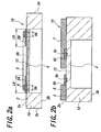
- Figs. 2(a) and 2(b) are sectional views of the embodiment in Fig. 1 taken along a IIa-IIa line and a IIb-IIb, respectively.
- a substrate 2 is made of and a ferrodielectric and electro-optic single crystal as mentioned above, in the form of an X- or Y-orientation.
- the substrate has opposed main planes 2a and 2b.
- an optical waveguide 3 of a Mach-Zehnder type having a given shape is formed on one main plane 2a.
- the optical waveguide 3 comprises an inlet portion 3a, branched portions 3b, 3c and a coupled portion 3d.
- Reference numerals 2c and 2d denote light inlet and outlet end faces of the substrate 2, respectively.
- a recess 4 having an almost rectangular-parallelepiped shape and opened at the other main plane, which defines a thinner portion 12 above the recess 4.
- a thicker portion is provided such that it surrounds the recess and the thinner portion 12 from four sides.
- Electrodes 6, 7 and 8 are formed on the main plane 2a of the substrate 2.
- the electrodes 6 and 8 function as ground electrodes, and the electrode 9 functions as a signal electrode.
- the main portion of the electrode 6 is provided above and substantially in parallel to the upper branched optical waveguide portion 3b, and opposite end portions of the electrode 6 extend down to a lower side of the substrate so that they may be electrically connected to a high frequency signal circuit (not shown).
- the main portion of the electrode 7 is provided between and substantially in parallel with the upper and lower branched optical waveguide portions 3b and 3c, and opposite end portions of the electrode 7 extend down to the lower side of the substrate within the opposite end portions of the electrode 6, so that they may be electrically connected to the high frequency signal circuit.
- the electrode 8 extend downwardly from beneath the branched optical waveguide 3c to the lower side of the substrate within the opposite end portions of the electrode 8, so that it may be electrically connected to the high frequency signal circuit.
- the electrode 8 has almost inverted trapezoidal shape having an upper side substantially in parallel with the branched optical waveguide 3c.
- an X plate or a Y plate made of lithium niobate is used as a substrate 2, for example. Therefore, a TE-mode light is transmitted in the optical waveguide.
- the branched portions 3b, 3c are provided in gap regions between the electrodes 6, 7 and 8, respectively.
- the optical waveguide 3 intersects with the electrodes 6 and 7 at six crossing portions 9A, 9B, 9C, 9D, 9E and 9F as viewed in plane. Each crossing portion exists on the thinner portion 12.
- Slender or band-shaped buffer layers 5A and 5B are formed on the branched optical waveguide 3b such that each of the buffer layers covers a part of the branched optical waveguide 3b.
- the buffer layers 5A and 5B are spaced from each other.
- the buffer layer 5A is interposed between the electrode 6 and the branched optical waveguide 3b at the crossing portion 9A.
- the buffer layer 5B is interposed between the electrode 6 and the branched optical waveguide 3b at the crossing portion 9B.
- Band-shaped buffer layers 5C and 5D are formed on the branched optical waveguide 3c such that each of the buffer layers covers a part of the branched optical waveguide 3c.
- the buffer layers 5C and 5D are spaced from each other.
- the buffer layer 5C is interposed between the electrode 6 and the branched optical waveguide 3c at the crossing portions 9C and between the electrode 7 and the branched optical waveguide 3c at the crossing portion 9E.
- the buffer layer 5D is interposed between the electrode 6 and the branched optical waveguide 3c at the crossing portions 9D and between the electrode 7 and the branched optical waveguide 3c at the crossing portion 9F.
- a plurality of the buffer layers are provided at the thinner portion, and each electrode passes on each of the buffer layers as shown in Fig. 1.
- plural rows of the optical waveguides are formed on the thinner portion, and each optical waveguide is partially covered with the buffer layer.
- differences among the covering lengths over which the buffer layers cover each of the optical waveguides are not more than 0.2 mm, more preferably almost equal to one another.
- the covering length (LA + LB) over which the branched optical waveguide 3b is covered with the buffer layers 5A and 5B is set equal to that (LC + LD) over which the branched optical waveguide 3c is covered with the buffer layers 5C and 5D.
- the buffer layer has a band shape, and the electrode extends crossing the band-shaped buffer layer.
- the DC drift resulting from the buffer layer can be minimized.
- the buffer layer is provided with a tapered zone at one end or both ends thereof, which gradually reduces its thickness when viewed in a longitudinal direction of the optical waveguide.
- Fig. 3 is a plane view showing a traveling wave optical modulator 1B having the above configuration
- Fig. 4 is a sectional view of the embodiment of Fig. 3 along a IV-IV line.
- the same or similar constituent parts are denoted by the same reference numerals in Figs. 1 and 2, and explanation on them will be omitted.
- a taper portion 13 is provided at each of both ends of each of the buffer layers 5E, 5F, 5G, 5H.
- the thickness of each buffer layer in the tapered portion gradually changes, i.e., decreases toward the end.
- a traveling wave optical modulator 1A as shown in Figs. 1, 2(a) and 2(b) was produced. More specifically, a wafer was prepared from a X-cut single crystal of LiNbO 3 , and its main planes were ground to a wafer thickness of 300 ⁇ m. A Mach-Zehnder type optical waveguide 3 was formed on one of the main planes, 2A, according to a titanium diffusion process and a photolithography. Next, buffer layers 5A to 5D were formed of silicon oxide as shown by using the photolithography method. Then, electrodes 6, 7 and 8 were formed of gold on the wafers, crossing the buffer layers as shown, respectively. The thus produced wafer was cut into traveling wave optical modulators with a dicing saw machine, and end faces of each optical waveguide 3 were optically polished.
- each of the main planes were coated with a photoresist film, and the optical modulator was set at an excimer laser machine in which a location of the optical modulator to be worked was aligned with reference to an orientation flat plane of the substrate.
- the other main plane 2b was worked through exposure to a light from a KrF excimer laser according to a spot scanning method.
- the optical system was adjusted so that the size of the irradiated spot was 1.0 mm in a scanning direction and 0.2 mm in width and an irradiating energy density of 6.0 J/cm 2 .
- a recess 4 was formed by working the substrate at a back side of the electrode with a laser at a pulse width of 15 nsec, a pulse frequency of 600 Hz and a scanning speed of 0.1 mm/sec.
- the thickness of the thicker portion of the optical waveguide substrate 2 was 300 ⁇ m, and that of the thinner portion 10 ⁇ m.
- the gap between the adjacent electrodes 6, 7 and 8 was 26 ⁇ .
- the width of the titanium pattern was 6 ⁇ m in forming the optical waveguide 3.
- Each buffer layer had the thickness of 0.4 ⁇ m, a width of 100 ⁇ m and a length of 0.2 mm.
- Those portions 9A to 9D of the electrode 6 crossing the buffer layers were each 50 ⁇ m, and those portions 9E and 9F of the electrode 7 crossing the buffer layers were each 50 ⁇ m.
- the thickness of each of the electrodes was 30 ⁇ m. Lengths LA, LB, LC and LD as shown were all 0.2 mm. Therefore, (LA + LB) was equal to (LC + LD).
- a traveling optical waveguide modulator was produced in the same manner as in Invention Example 1, provided that no buffer layers 5A to 5D were provided.
- the light absorption loss can be suppressed in the traveling wave optical modulator having the thinner portion and the thicker portion, which modulator can perform optical modulator at a high speed.
Landscapes
- Physics & Mathematics (AREA)
- Nonlinear Science (AREA)
- General Physics & Mathematics (AREA)
- Optics & Photonics (AREA)
- Chemical & Material Sciences (AREA)
- Engineering & Computer Science (AREA)
- Ceramic Engineering (AREA)
- Crystallography & Structural Chemistry (AREA)
- Optical Modulation, Optical Deflection, Nonlinear Optics, Optical Demodulation, Optical Logic Elements (AREA)
- Optical Integrated Circuits (AREA)
Abstract
Description
- The present invention relates to traveling wave optical modulators.
- NGK Insulators, Ltd. reported in JP-A 10-133,159 that a traveling wave optical modulator was successfully operated at not less than 10 GHz by providing a thinner portion in a substrate of the modulator under an optical waveguide and setting the thickness of this thinner portion to not more than 10 µm, while providing no buffer layer made of silicon oxide or the like. In this manner, the optical waveguide substrate advantageously comprises such thick and thinner portions, because optical modulation is possible at high speeds without the formation of the buffer layer, a DC drift originating from the buffer layer can be avoided, and a product (Vπ · L) between a driving voltage Vπ and the length L of an electrode can be reduced.
- However, NGK more specifically examined traveling wave optical modulators of this type, and then found that light absorption loss sometimes occurred in the optical waveguide. Particularly when the optical waveguides of the Mach-Zehnder type is formed, it is necessary that the optical waveguide is branched into two lines, and that lights, which come out from the branched optical waveguides are coupled together again, so that the absorption loss in each of the branched optical waveguide needs to be the same. However, the absorbing loss of one branched optical waveguide actually differed from that of the other, which might result in reduction in the extinction ratio.
- It is an object of the present invention to suppress the absorption loss of the light in the optical waveguide in the traveling wave optical modulator, which can effect optical modulation at a high speed, and reduce a DC drift and a product (Vπ · L) between a driving voltage Vπ and the length L of an electrode.
- The present inventors succeeded in suppressing the absorption loss in a traveling wave optical modulator, by constructing the modulator from (a) an optical waveguide substrate made of an electro-optic and ferrodielectric single crystal in the form of an X- or Y-orientation plate_and comprising a thicker portion having a larger thickness and a thinner portion having a smaller thickness; (b) first and second branched optical waveguide portions formed at least on the thinner portion of the optical waveguide substrate; (c) a set of electrodes provided on at least the thinner portion of the substrate and adapted for applying voltage to the first and second optical waveguide portions to modulate a light propagating the optical waveguide portions; and (d) a buffer layer provided to cover a part of the optical waveguide portions at the thinner portion of the substrate, the electrodes crossing the waveguide portions on the buffer layer.
- These and other objects, features and advantages of the invention will be well appreciated upon reading the following description of the invention when taken in conjunction with the attached drawings, with the understanding that some modifications, variations and changes of the invention could be easily made by the skilled person in the art to which the invention pertains.
- For a better understanding of the present invention, reference is made to the attached drawings, wherein:
- Fig. 1 is a plane view schematically showing one
embodiment 1A of the traveling wave optical waveguide according to the present invention; - Figs. 2(a) and 2(b) are sectional views of the embodiment in Fig. 1 taken along a IIa-IIa line and a IIb-IIb, respectively;
- Fig. 3 is a plane view schematically showing another
embodiment 1B of the traveling wave optical waveguide according to the present invention; and - Fig. 4 is a sectional view of the embodiment in Fig. 4 along with a IV-IV line.
-
- In the present invention, the substrate is made of an electro-optic and ferrodielectric single crystal having a given shape, e.g., in the form of an X- or Y-orientation plate. So long as the crystal can be optically modulated, no limitation is posed. For example, lithium niobate, potassium lithium niobate, lithium tantalate, KTP, glass, silicon, GaAs and quartz may be recited. At least one single crystal selected from the group consisting of a single crystal of lithium niobate, a single crystal of lithium tantalate and a solid solution single crystal of lithium niobate-lithium tantalate is particularly preferred.
- The substrate has opposed main planes, and an
optical waveguide 3 of a Mach-Zehnder type is formed on one of the opposed main planes. A recess is formed in the other main plane having an almost rectangular parallelepiped shape, opening in the other main plane. Thus, a thinner portion is defined, corresponding to the recess, while a thicker portion is provided around the thinner portion, for example. A set of electrodes are provided on at least the thinner portion of said one main plane of the substrate for applying voltage to the first and second optical waveguide portions of the optical waveguide to modulate a light propagating the optical waveguide portions. - A buffer layer is provided to cover a part of the optical waveguide portions at the thinner portion of the substrate, the electrodes crossing on the buffer layer.
- In the present invention, the following (1) to (4) are preferred. Any combination of (1) to (4) may be considered as preferable embodiments, so long as no contradiction occurs.
(1)Pural buffer layers are provided at respectively plural portions which the electrodes cross. By so doing, the optical absorption loss in one optical waveguide portion can be approached to that in the other. It is preferable that a deviation between a total length of said plural buffer layers in one optical waveguide portion as extending along the optical waveguide portion and that of said plural buffer layers in the optical waveguide portion as extending along the optical waveguide portion is reduced to a low level, preferably not more than 0.2 mm, and more preferably the former length is substantially equal to the latter.
(2) Each of said plural buffer layers has such a band-like shape as extending along the optical waveguide portion. By adopting the buffer layers having such a shape, the DC drift resulting from the buffer layers can be minimized.
(3) At least one end portion of the buffer layer or at least one buffer layer as viewed along the optical waveguide portions is provided with a taper portion of which thickness gradually changes as viewed along the optical waveguide. By so constructing, occurrence of a discontinuous point where a characteristic impedance sharply changes can be prevented. Further, since no rapid mode (opto-electro field) change does not occurs, reflection of light under the buffer layer can be prevented.
(4) The traveling wave optical modulator is adapted to pass a TE mode light through the optical waveguide portions. - The thickness of the thicker portion is preferably not less than 300 µm from the point of view of affording strength upon the optical waveguide substrate.
- The thickness of the thinner portion is preferably not more than 20 µm, more preferably not more than 10 µm, from the standpoint of view of conspicuously reducing the effective refractive index of the microwaves. Further, this thickness is preferably not less than 5 µm from the standpoint of view of preventing cracking on working the thinner portion.
- The thickness of the buffer layer is preferably not less than 0.3 µm from the standpoint of view of suppressing the absorption loss of the light propagating the optical waveguide. On the other hand, the thickness of the buffer layer is preferably not more than 1.5 µm from the standpoint of view of suppressing the DC drift.
- The electrodes are not limited to any material, so long as it has a low resistance and an excellent characteristic impedance. The electrodes may be made of gold, silver or copper, etc.
- As the buffer layer, a known material such as silicon oxide, magnesium fluoride, silicon nitride or alumina may be used. The buffer layer may be formed by a known method such as a lithography method.
- The present invention will be explained in more detail with reference to Figs. 1,2(a) and 2(b). Fig. 1 is a plan view schematically showing one
embodiment 1A of the traveling wave optical waveguide modulator according to the present invention, and Figs. 2(a) and 2(b) are sectional views of the embodiment in Fig. 1 taken along a IIa-IIa line and a IIb-IIb, respectively. - A
substrate 2 is made of and a ferrodielectric and electro-optic single crystal as mentioned above, in the form of an X- or Y-orientation. The substrate has opposedmain planes optical waveguide 3 of a Mach-Zehnder type having a given shape is formed on onemain plane 2a. In the present embodiment, theoptical waveguide 3 comprises aninlet portion 3a,branched portions portion 3d.Reference numerals substrate 2, respectively. - In a central portion of the
substrate 2 is formed arecess 4 having an almost rectangular-parallelepiped shape and opened at the other main plane, which defines athinner portion 12 above therecess 4. A thicker portion is provided such that it surrounds the recess and thethinner portion 12 from four sides.Electrodes main plane 2a of thesubstrate 2. Theelectrodes electrode 6 is provided above and substantially in parallel to the upper branchedoptical waveguide portion 3b, and opposite end portions of theelectrode 6 extend down to a lower side of the substrate so that they may be electrically connected to a high frequency signal circuit (not shown). The main portion of theelectrode 7 is provided between and substantially in parallel with the upper and lower branchedoptical waveguide portions electrode 7 extend down to the lower side of the substrate within the opposite end portions of theelectrode 6, so that they may be electrically connected to the high frequency signal circuit. Theelectrode 8 extend downwardly from beneath the branchedoptical waveguide 3c to the lower side of the substrate within the opposite end portions of theelectrode 8, so that it may be electrically connected to the high frequency signal circuit. Theelectrode 8 has almost inverted trapezoidal shape having an upper side substantially in parallel with the branchedoptical waveguide 3c. - In the present embodiment, an X plate or a Y plate made of lithium niobate is used as a
substrate 2, for example. Therefore, a TE-mode light is transmitted in the optical waveguide. Thebranched portions electrodes - In this embodiment, the
optical waveguide 3 intersects with theelectrodes crossing portions thinner portion 12. - Slender or band-shaped buffer layers 5A and 5B are formed on the branched
optical waveguide 3b such that each of the buffer layers covers a part of the branchedoptical waveguide 3b. The buffer layers 5A and 5B are spaced from each other. Thebuffer layer 5A is interposed between theelectrode 6 and the branchedoptical waveguide 3b at thecrossing portion 9A. Thebuffer layer 5B is interposed between theelectrode 6 and the branchedoptical waveguide 3b at the crossingportion 9B. - Band-shaped
buffer layers optical waveguide 3c such that each of the buffer layers covers a part of the branchedoptical waveguide 3c. The buffer layers 5C and 5D are spaced from each other. Thebuffer layer 5C is interposed between theelectrode 6 and the branchedoptical waveguide 3c at thecrossing portions 9C and between theelectrode 7 and the branchedoptical waveguide 3c at the crossingportion 9E. - The
buffer layer 5D is interposed between theelectrode 6 and the branchedoptical waveguide 3c at thecrossing portions 9D and between theelectrode 7 and the branchedoptical waveguide 3c at thecrossing portion 9F. - In this way, only a part of the optical waveguide is covered with the buffer layers, and the electrodes are passed on the buffer layers. Consequently, the absorption loss of the light propagating through the optical waveguide is successfully suppressed.
In addition, it is confirmed that this does not adversely affect the high-speed modulating characteristic, or cause the DC drift resulting from the buffer layers. - In a preferred embodiment, a plurality of the buffer layers are provided at the thinner portion, and each electrode passes on each of the buffer layers as shown in Fig. 1.
- Further, plural rows of the optical waveguides are formed on the thinner portion, and each optical waveguide is partially covered with the buffer layer. By this construction, the amount of the light absorption loss can be approached among the optical waveguides.
- In this case, it is particularly preferable that differences among the covering lengths over which the buffer layers cover each of the optical waveguides are not more than 0.2 mm, more preferably almost equal to one another. For example, in the embodiment of Fig. 1, the covering length (LA + LB) over which the branched
optical waveguide 3b is covered with the buffer layers 5A and 5B is set equal to that (LC + LD) over which the branchedoptical waveguide 3c is covered with the buffer layers 5C and 5D. By this construction, the light absorption losses in the optical waveguides can be made equal to each other or one another, thereby improving the extinction ratio. - Preferably, the buffer layer has a band shape, and the electrode extends crossing the band-shaped buffer layer. By adopting the thus configurated buffer layer, the DC drift resulting from the buffer layer can be minimized.
- In a particularly preferred embodiment of the present invention, the buffer layer is provided with a tapered zone at one end or both ends thereof, which gradually reduces its thickness when viewed in a longitudinal direction of the optical waveguide. By this construction, occurrence of a discontinuous point where the characteristic impedance rapidly changes can be prevented. Further, since the light does not undergo rapid mode change (optoelectric fieldduring passage immediately under the buffer layer, the reflection of the light under the buffer layer can be prevented.

- Fig. 3 is a plane view showing a traveling wave
optical modulator 1B having the above configuration, and Fig. 4 is a sectional view of the embodiment of Fig. 3 along a IV-IV line. In Figs. 3 and 4, the same or similar constituent parts are denoted by the same reference numerals in Figs. 1 and 2, and explanation on them will be omitted. - In the traveling wave
optical modulator 1B according to this embodiment, ataper portion 13 is provided at each of both ends of each of the buffer layers 5E, 5F, 5G, 5H. The thickness of each buffer layer in the tapered portion gradually changes, i.e., decreases toward the end. - In the following, the present invention will be explained in more detail with reference to specific examples.
- A traveling wave
optical modulator 1A as shown in Figs. 1, 2(a) and 2(b) was produced. More specifically, a wafer was prepared from a X-cut single crystal of LiNbO3, and its main planes were ground to a wafer thickness of 300 µm. A Mach-Zehnder typeoptical waveguide 3 was formed on one of the main planes, 2A, according to a titanium diffusion process and a photolithography. Next, buffer layers 5A to 5D were formed of silicon oxide as shown by using the photolithography method. Then,electrodes optical waveguide 3 were optically polished. - Next, each of the main planes were coated with a photoresist film, and the optical modulator was set at an excimer laser machine in which a location of the optical modulator to be worked was aligned with reference to an orientation flat plane of the substrate. The other
main plane 2b was worked through exposure to a light from a KrF excimer laser according to a spot scanning method. The optical system was adjusted so that the size of the irradiated spot was 1.0 mm in a scanning direction and 0.2 mm in width and an irradiating energy density of 6.0 J/cm2. Arecess 4 was formed by working the substrate at a back side of the electrode with a laser at a pulse width of 15 nsec, a pulse frequency of 600 Hz and a scanning speed of 0.1 mm/sec. - The thickness of the thicker portion of the
optical waveguide substrate 2 was 300 µm, and that of thethinner portion 10 µm. The gap between theadjacent electrodes optical waveguide 3. Each buffer layer had the thickness of 0.4 µm, a width of 100 µm and a length of 0.2 mm. Thoseportions 9A to 9D of theelectrode 6 crossing the buffer layers were each 50 µm, and thoseportions electrode 7 crossing the buffer layers were each 50 µm. The thickness of each of the electrodes was 30 µm. Lengths LA, LB, LC and LD as shown were all 0.2 mm. Therefore, (LA + LB) was equal to (LC + LD). - A traveling optical waveguide modulator was produced in the same manner as in Invention Example 1, provided that no buffer layers 5A to 5D were provided.
- Twenty eight traveling wave optical modulators were prepared in each of Invention Example 1 and Comparative Example. Single core fiber arrays each having a single mode optical fiber for 1.5 µm wavelength use were prepared, and coupled with respective modulators, and bonded thereto with an ultraviolet light-curable resin in the state that the optical fiber was aligned with the optical waveguide. With respect to the modulators in Invention Example and Comparative Example, the insertion loss was measured, and results are shown in Table 1.
Optical insertion loss (n=28) Average value Difference between upper and lower values Invention Example 1 3.9 dB 0.4 dB Comparative Example 9.7 dB 0.8 dB - Experiment B was conducted as in Invention Example 1, provided that LA and LB were 0.15 mm and 0.25 mm, respectively, while LC and LD were both 0.25 mm. Therefore, (LA + LB) = 0.4 mm, and (LC + LD) = 0.5 mm. This was taken as Invention Example 2.
- With respect to each of Comparative Example and Invention Example 1 in Experiment B and the above Invention Example 2, sixteen traveling optical waveguide modulators were produced. Then, as in Experiment A, optical fibers were coupled with the respective modulators, and then an on-off extinction ratio was measured.
Results are shown in Table 2.On-off extinction ratio ( n= 16) Average value Difference between upper and lower values Invention Example 1 24.6 dB 3.2 dB Invention Example 2 23.4 dB 2.8 dB Comparative Example 12.3 dB 2.8 dB - As mentioned above according to the present invention, the light absorption loss can be suppressed in the traveling wave optical modulator having the thinner portion and the thicker portion, which modulator can perform optical modulator at a high speed.
Claims (5)
- A traveling wave optical modulator comprising:an optical waveguide substrate made of an electro-optic and ferrodielectric single crystal in the form of an X- or Y-orientation plate_and comprising a thicker portion having a larger thickness and a thinner portion having a smaller thickness;first and second branched optical waveguide portions formed at least on the thinner portion of the optical waveguide substrate;a set of electrodes provided on at least the thinner portion of the substrate and adapted for applying voltage to the first and second optical waveguide portions to modulate a light propagating the optical waveguide portions; anda buffer layer provided to cover a part of the optical waveguide portions at the thinner portion of the substrate, the electrodes crossing on the buffer layer.
- The traveling wave optical modulator set forth in claim 1, wherein plural buffer layers are provided at respectively plural portions which the electrodes cross, and a deviation between a total length of said plural buffer layers in one optical waveguide portion as extending along the optical waveguide portion and that of said plural buffer layers in the optical waveguide portion as extending along the optical waveguide portion is not more than 0.2 mm.
- The traveling wave optical modulator set forth in claim 2, wherein each of said plural buffer layers has such a band-like shape as extending along the optical waveguide portion.
- The traveling wave optical modulator set forth in any one of claims 1 to 3, wherein at least one end portion of the buffer layer or at least one buffer layer as viewed along the optical waveguide portions is provided with a taper portion of which thickness gradually changes as viewed along the optical waveguide.
- The traveling wave optical modulator set forth in any one of claims 1 to 4, which is adapted to pass a TE mode light through the optical waveguide portions.
Applications Claiming Priority (2)
| Application Number | Priority Date | Filing Date | Title |
|---|---|---|---|
| JP35533599 | 1999-12-15 | ||
| JP35533599A JP2001174765A (en) | 1999-12-15 | 1999-12-15 | Traveling waveform light modulator |
Publications (2)
| Publication Number | Publication Date |
|---|---|
| EP1109050A1 true EP1109050A1 (en) | 2001-06-20 |
| EP1109050B1 EP1109050B1 (en) | 2003-05-02 |
Family
ID=18443347
Family Applications (1)
| Application Number | Title | Priority Date | Filing Date |
|---|---|---|---|
| EP00311093A Expired - Lifetime EP1109050B1 (en) | 1999-12-15 | 2000-12-13 | Travelling wave optical modulators |
Country Status (4)
| Country | Link |
|---|---|
| US (1) | US6539130B2 (en) |
| EP (1) | EP1109050B1 (en) |
| JP (1) | JP2001174765A (en) |
| DE (1) | DE60002421T2 (en) |
Cited By (4)
| Publication number | Priority date | Publication date | Assignee | Title |
|---|---|---|---|---|
| US6556727B2 (en) * | 2000-09-22 | 2003-04-29 | Ngk Insulators, Ltd. | Travelling wave-type optical modulator |
| EP1335237A1 (en) * | 2002-02-08 | 2003-08-13 | Fujitsu Limited | Electrical connection of an electro-optic element |
| EP1486817A4 (en) * | 2002-03-19 | 2005-08-17 | Ngk Insulators Ltd | Method of manufacturing optical modulator |
| US9366825B2 (en) | 2010-03-29 | 2016-06-14 | Sumitomo Osaka Cement Co., Ltd. | Optical waveguide device module |
Families Citing this family (15)
| Publication number | Priority date | Publication date | Assignee | Title |
|---|---|---|---|---|
| JP3954251B2 (en) * | 1999-08-27 | 2007-08-08 | 日本碍子株式会社 | Traveling waveform light modulator |
| US6600843B2 (en) | 2001-03-13 | 2003-07-29 | Srico, Inc. | Optical modulator |
| JP4875807B2 (en) * | 2001-08-01 | 2012-02-15 | 住友大阪セメント株式会社 | Light modulator |
| US7272271B2 (en) * | 2001-09-26 | 2007-09-18 | Celight, Inc. | Electro-optical integrated transmitter chip for arbitrary quadrature modulation of optical signals |
| JP5055947B2 (en) * | 2006-10-20 | 2012-10-24 | 富士通オプティカルコンポーネンツ株式会社 | Optical modulator and transmitter |
| JP5166450B2 (en) * | 2008-01-31 | 2013-03-21 | 日本碍子株式会社 | Optical waveguide device |
| JP5001310B2 (en) * | 2009-02-03 | 2012-08-15 | 日本電信電話株式会社 | Light modulator |
| US20130170781A1 (en) * | 2011-12-28 | 2013-07-04 | Karl Kissa | Y-branch dual optical phase modulator |
| US9804475B1 (en) | 2015-04-16 | 2017-10-31 | Aurrion, Inc. | Radio-frequency loss reduction in photonic circuits |
| JP6475838B2 (en) * | 2015-08-04 | 2019-02-27 | 日本電信電話株式会社 | Light modulator |
| JP2017167463A (en) * | 2016-03-18 | 2017-09-21 | セイコーエプソン株式会社 | Optical modulator and image display apparatus |
| JP7434843B2 (en) * | 2019-11-28 | 2024-02-21 | 住友大阪セメント株式会社 | Optical waveguide elements, optical modulators, optical modulation modules, and optical transmitters |
| JP7334616B2 (en) * | 2019-12-26 | 2023-08-29 | 住友大阪セメント株式会社 | Optical waveguide element, optical modulator, optical modulation module, and optical transmitter |
| JP7632101B2 (en) * | 2021-06-11 | 2025-02-19 | 住友電気工業株式会社 | Optical modulator and method for manufacturing optical modulator |
| JP7739782B2 (en) | 2021-06-24 | 2025-09-17 | 住友大阪セメント株式会社 | Optical waveguide element, optical modulator, optical modulation module, and optical transmitter |
Citations (4)
| Publication number | Priority date | Publication date | Assignee | Title |
|---|---|---|---|---|
| JPS61198133A (en) * | 1985-02-27 | 1986-09-02 | Fujitsu Ltd | Waveguide type optical switch |
| EP0485993A1 (en) * | 1990-11-14 | 1992-05-20 | Oki Electric Industry Co., Ltd. | Waveguide-type optical device |
| JPH04204815A (en) * | 1990-11-30 | 1992-07-27 | Matsushita Electric Ind Co Ltd | Optical waveguide modulator and production thereof |
| EP0828175A2 (en) * | 1996-09-06 | 1998-03-11 | Ngk Insulators, Ltd. | Optical waveguide devices, travelling-wave light modulators, and process for producing optical waveguide device |
Family Cites Families (5)
| Publication number | Priority date | Publication date | Assignee | Title |
|---|---|---|---|---|
| US6167169A (en) * | 1994-09-09 | 2000-12-26 | Gemfire Corporation | Scanning method and architecture for display |
| US6198855B1 (en) * | 1996-07-19 | 2001-03-06 | Jds Uniphase Corporation | Velocity-matched, traveling-wave electro-optical devices using non-conductive and conductive polymer buffer layers |
| US6226423B1 (en) * | 1998-09-11 | 2001-05-01 | Ngk Insulators, Ltd. | Optical waveguide element |
| US6069729A (en) * | 1999-01-20 | 2000-05-30 | Northwestern University | High speed electro-optic modulator |
| US6341031B1 (en) * | 1999-05-25 | 2002-01-22 | Jds Uniphase Corporation | Optical pulse generation using a high order function waveguide interferometer |
-
1999
- 1999-12-15 JP JP35533599A patent/JP2001174765A/en active Pending
-
2000
- 2000-12-13 EP EP00311093A patent/EP1109050B1/en not_active Expired - Lifetime
- 2000-12-13 DE DE60002421T patent/DE60002421T2/en not_active Expired - Lifetime
- 2000-12-15 US US09/738,174 patent/US6539130B2/en not_active Expired - Fee Related
Patent Citations (4)
| Publication number | Priority date | Publication date | Assignee | Title |
|---|---|---|---|---|
| JPS61198133A (en) * | 1985-02-27 | 1986-09-02 | Fujitsu Ltd | Waveguide type optical switch |
| EP0485993A1 (en) * | 1990-11-14 | 1992-05-20 | Oki Electric Industry Co., Ltd. | Waveguide-type optical device |
| JPH04204815A (en) * | 1990-11-30 | 1992-07-27 | Matsushita Electric Ind Co Ltd | Optical waveguide modulator and production thereof |
| EP0828175A2 (en) * | 1996-09-06 | 1998-03-11 | Ngk Insulators, Ltd. | Optical waveguide devices, travelling-wave light modulators, and process for producing optical waveguide device |
Non-Patent Citations (3)
| Title |
|---|
| BULMER C H ET AL: "PHASE TUNING OF LINBO3 INTERFEROMETRIC MODULTORS BY LASER ABLATION", INTEGRATED PHOTONICS RESEARCH. TECHNICAL DIGEST SERIES,US,WASHINGTON, DC, VOL. 8, PAGE(S) 63, XP000350621 * |
| PATENT ABSTRACTS OF JAPAN vol. 011, no. 026 (P - 539) 24 January 1987 (1987-01-24) * |
| PATENT ABSTRACTS OF JAPAN vol. 016, no. 540 (P - 1450) 10 November 1992 (1992-11-10) * |
Cited By (5)
| Publication number | Priority date | Publication date | Assignee | Title |
|---|---|---|---|---|
| US6556727B2 (en) * | 2000-09-22 | 2003-04-29 | Ngk Insulators, Ltd. | Travelling wave-type optical modulator |
| EP1335237A1 (en) * | 2002-02-08 | 2003-08-13 | Fujitsu Limited | Electrical connection of an electro-optic element |
| EP1486817A4 (en) * | 2002-03-19 | 2005-08-17 | Ngk Insulators Ltd | Method of manufacturing optical modulator |
| US7290328B2 (en) | 2002-03-19 | 2007-11-06 | Ngk Insulators, Ltd. | Method of manufacturing optical modulator |
| US9366825B2 (en) | 2010-03-29 | 2016-06-14 | Sumitomo Osaka Cement Co., Ltd. | Optical waveguide device module |
Also Published As
| Publication number | Publication date |
|---|---|
| DE60002421D1 (en) | 2003-06-05 |
| US20010007601A1 (en) | 2001-07-12 |
| DE60002421T2 (en) | 2004-03-25 |
| JP2001174765A (en) | 2001-06-29 |
| EP1109050B1 (en) | 2003-05-02 |
| US6539130B2 (en) | 2003-03-25 |
Similar Documents
| Publication | Publication Date | Title |
|---|---|---|
| EP1109050B1 (en) | Travelling wave optical modulators | |
| JP4471520B2 (en) | Traveling waveform light modulator | |
| JP2583480B2 (en) | Optical switch and optical switch array | |
| EP1722266B1 (en) | A travelling wave-type optical modulator | |
| JP2955986B2 (en) | Semiconductor optical modulator and method of manufacturing the same | |
| US8923658B2 (en) | Optical waveguide device | |
| EP1079257B1 (en) | Travelling wave optical modulator | |
| EP1542063B1 (en) | Mechanical stress reduction in an electro-optical optical modulator | |
| JP4874685B2 (en) | Light modulator | |
| US11086149B2 (en) | Electro-optic device | |
| JPH07234391A (en) | Light control device | |
| JP2001051244A (en) | Optical modulator using photonic bandgap structure and optical modulation method | |
| CN100447615C (en) | Optical waveguide device and traveling wave type optical modulator | |
| US12085791B2 (en) | Optical waveguide element and optical modulation element | |
| EP0905543B1 (en) | Light modulators | |
| JP4587509B2 (en) | Waveguide type optical modulator | |
| JP3995537B2 (en) | Light modulator | |
| EP1193536B1 (en) | A travelling wave-type optical modulator | |
| JP2000275590A (en) | Waveguide type optical modulator | |
| US12164185B2 (en) | Optical modulation element | |
| CN115407529A (en) | Optical waveguide element, optical modulator, optical modulation module, and optical transmission device | |
| JPH09185025A (en) | Light control element | |
| JP2007264543A (en) | Waveguide type optical device | |
| WO2025203412A1 (en) | Optical waveguide element, optical modulator, and optical transmission device | |
| JP2010038951A (en) | Optical modulator |
Legal Events
| Date | Code | Title | Description |
|---|---|---|---|
| PUAI | Public reference made under article 153(3) epc to a published international application that has entered the european phase |
Free format text: ORIGINAL CODE: 0009012 |
|
| AK | Designated contracting states |
Kind code of ref document: A1 Designated state(s): DE FR GB IT |
|
| AX | Request for extension of the european patent |
Free format text: AL;LT;LV;MK;RO;SI |
|
| 17P | Request for examination filed |
Effective date: 20011213 |
|
| AKX | Designation fees paid |
Free format text: DE FR GB IT |
|
| GRAG | Despatch of communication of intention to grant |
Free format text: ORIGINAL CODE: EPIDOS AGRA |
|
| 17Q | First examination report despatched |
Effective date: 20020627 |
|
| GRAG | Despatch of communication of intention to grant |
Free format text: ORIGINAL CODE: EPIDOS AGRA |
|
| GRAG | Despatch of communication of intention to grant |
Free format text: ORIGINAL CODE: EPIDOS AGRA |
|
| GRAH | Despatch of communication of intention to grant a patent |
Free format text: ORIGINAL CODE: EPIDOS IGRA |
|
| GRAH | Despatch of communication of intention to grant a patent |
Free format text: ORIGINAL CODE: EPIDOS IGRA |
|
| GRAA | (expected) grant |
Free format text: ORIGINAL CODE: 0009210 |
|
| AK | Designated contracting states |
Designated state(s): DE FR GB IT |
|
| REG | Reference to a national code |
Ref country code: GB Ref legal event code: FG4D |
|
| REF | Corresponds to: |
Ref document number: 60002421 Country of ref document: DE Date of ref document: 20030605 Kind code of ref document: P |
|
| ET | Fr: translation filed | ||
| PLBE | No opposition filed within time limit |
Free format text: ORIGINAL CODE: 0009261 |
|
| STAA | Information on the status of an ep patent application or granted ep patent |
Free format text: STATUS: NO OPPOSITION FILED WITHIN TIME LIMIT |
|
| 26N | No opposition filed |
Effective date: 20040203 |
|
| PGFP | Annual fee paid to national office [announced via postgrant information from national office to epo] |
Ref country code: FR Payment date: 20101203 Year of fee payment: 11 |
|
| PGFP | Annual fee paid to national office [announced via postgrant information from national office to epo] |
Ref country code: GB Payment date: 20101123 Year of fee payment: 11 |
|
| GBPC | Gb: european patent ceased through non-payment of renewal fee |
Effective date: 20111213 |
|
| REG | Reference to a national code |
Ref country code: FR Ref legal event code: ST Effective date: 20120831 |
|
| PG25 | Lapsed in a contracting state [announced via postgrant information from national office to epo] |
Ref country code: GB Free format text: LAPSE BECAUSE OF NON-PAYMENT OF DUE FEES Effective date: 20111213 |
|
| PG25 | Lapsed in a contracting state [announced via postgrant information from national office to epo] |
Ref country code: FR Free format text: LAPSE BECAUSE OF NON-PAYMENT OF DUE FEES Effective date: 20120102 |
|
| PGFP | Annual fee paid to national office [announced via postgrant information from national office to epo] |
Ref country code: DE Payment date: 20131211 Year of fee payment: 14 |
|
| PGFP | Annual fee paid to national office [announced via postgrant information from national office to epo] |
Ref country code: IT Payment date: 20131107 Year of fee payment: 14 |
|
| REG | Reference to a national code |
Ref country code: DE Ref legal event code: R119 Ref document number: 60002421 Country of ref document: DE |
|
| PG25 | Lapsed in a contracting state [announced via postgrant information from national office to epo] |
Ref country code: DE Free format text: LAPSE BECAUSE OF NON-PAYMENT OF DUE FEES Effective date: 20150701 |
|
| PG25 | Lapsed in a contracting state [announced via postgrant information from national office to epo] |
Ref country code: IT Free format text: LAPSE BECAUSE OF NON-PAYMENT OF DUE FEES Effective date: 20141213 |