EP1107642A2 - Condenser microphone - Google Patents
Condenser microphone Download PDFInfo
- Publication number
- EP1107642A2 EP1107642A2 EP00306107A EP00306107A EP1107642A2 EP 1107642 A2 EP1107642 A2 EP 1107642A2 EP 00306107 A EP00306107 A EP 00306107A EP 00306107 A EP00306107 A EP 00306107A EP 1107642 A2 EP1107642 A2 EP 1107642A2
- Authority
- EP
- European Patent Office
- Prior art keywords
- fet
- circuit board
- printed circuit
- condenser microphone
- polar plate
- Prior art date
- Legal status (The legal status is an assumption and is not a legal conclusion. Google has not performed a legal analysis and makes no representation as to the accuracy of the status listed.)
- Withdrawn
Links
Images


Classifications
-
- H—ELECTRICITY
- H04—ELECTRIC COMMUNICATION TECHNIQUE
- H04R—LOUDSPEAKERS, MICROPHONES, GRAMOPHONE PICK-UPS OR LIKE ACOUSTIC ELECTROMECHANICAL TRANSDUCERS; DEAF-AID SETS; PUBLIC ADDRESS SYSTEMS
- H04R19/00—Electrostatic transducers
-
- H—ELECTRICITY
- H03—ELECTRONIC CIRCUITRY
- H03K—PULSE TECHNIQUE
- H03K19/00—Logic circuits, i.e. having at least two inputs acting on one output; Inverting circuits
- H03K19/01—Modifications for accelerating switching
-
- H—ELECTRICITY
- H05—ELECTRIC TECHNIQUES NOT OTHERWISE PROVIDED FOR
- H05K—PRINTED CIRCUITS; CASINGS OR CONSTRUCTIONAL DETAILS OF ELECTRIC APPARATUS; MANUFACTURE OF ASSEMBLAGES OF ELECTRICAL COMPONENTS
- H05K1/00—Printed circuits
- H05K1/02—Details
- H05K1/14—Structural association of two or more printed circuits
- H05K1/141—One or more single auxiliary printed circuits mounted on a main printed circuit, e.g. modules, adapters
Definitions
- the present invention relates to a condenser microphone capable of converting the variation of capacitance caused by sound wave into an electrical signal.
- Embodiments of the condenser microphone are capable of achieving automation in a manufacturing process and reducing the damage of a field effect transistor (hereinafter, referred to as 'FET') during the manufacturing process.
- 'FET' field effect transistor
- a conventional condenser microphone comprises a printed circuit board 101, an FET 102 for converting the change of electric potential due to the variation of capacitance into an electrical signal, a base 103, a polar plate 104 on which a plurality of through holes are formed, a spacer 106, a polar ring 108, a diaphragm 107 being vibrated by the sound wave flowing therein, and a case 109 on which a sound wave inflow hole 110 is drilled.
- the conventional condenser microphone is manufactured in such a manner that after the polar ring 108, the diaphragm 107, the spacer 106 and the polar plate 104 are sequentially assembled in the case 109, and the printed circuit board 101 on which the FET 102 is coupled is finally assembled therein, the one end of the case 109 is folded.
- the gate of the FET 102 is electrically connected to the polar plate 104, and the source and drain thereof are exposed to the outside of the printed circuit board 101.
- the source and drain of the FET 102 are folded downward to be inserted into the through holes of the printed circuit board 101.
- the source and drain of the FET 102 are again folded to surround the printed circuit board 101.
- the gate of the FET 102 is folded upward such that upon assembling the FET 102 in the case 109, it is connected to the polar plate 104.
- the source and drain of the FET 102 should be folded back to the original state thereof after a manufacturing process.
- connection failure may be caused.
- An embodiment of the invention provides a condenser microphone capable of realizing the automation of a manufacturing process by the connection of a FET to a printed circuit board by cream soldering and reducing the damage of the FET during the manufacturing process to improve production efficiency thereof.
- Another embodiment of the invention provides a condenser microphone capable of improving the connection method of a polar plate and a FET to prevent connection failure between the polar plate and the gate of the FET.
- a condenser microphone constructed to convert the variation of capacitance between a diaphragm and a polar plate caused by sound wave into an electrical signal, which comprises: a printed circuit board having predetermined patterns formed on the both surfaces thereof and connected to each terminal of an FET; a metal ring for electrically connecting the gate of the FET and the polar plate; and a case electrically connected to a polar ring and for electrically connecting the diaphragm vibrated by the sound wave to the source of the FET.
- the each terminal of the FET is connected to each pattern of the printed circuit board in such a manner that the gate thereof is folded and soldered to be connected to one of the patterns of the printed circuit board and the source and drain thereof are inserted to be passed through the printed circuit board and then soldered to be connected to ones of the patterns thereof.
- the base ring of an insulation material should be interposed between the metal ring and the case, and a spacer of an insulation material should be interposed between the polar plate and the diaphragm so that the polar plate and the diaphragm are insulated and spaced out a predetermine distance apart from each other.
- the condenser microphone according to the present invention is configured, as shown in Figs. 3 and 4, in such a manner that the gate of an FET 2, which is connected to a pattern 1G of a printed circuit board 1, and the source and drain of the FET, which are inserted into the through holes 1a and 1b of the printed circuit board 1 are soldered by means of cream or soft solder, to the pattern 1G, 1S, 1D thereof respectively.
- the predetermined patterns 1G, 1S, 1D are formed to be connected to each terminal of the FET 2 and a metal ring 3, and as the pattern 1G connected to the gate of the FET 2 is the one which is electrically connected to the pattern connected to the metal ring 3, it is denoted by the same reference numeral.
- the through holes 1a and 1b are drilled through the printed circuit board 1 from top to bottom.
- the pattern 1S is formed to be electrically connected to the source of the FET 2, i.e. ground of the FET 2, as well as to the case 9.
- the metal ring 3 made of a conductive material, a base ring 3 of an insulation material, a polar plate 5 on which a plurality of holes are drilled, a spacer of an insulation material, a diaphragm 7 of a high molecular film and a polar ring 8 are electrically connected or built up to be insulated from each other.
- a case 9 through which a sound wave inflow hole 10 is drilled is folded to surround the circumference of the printed circuit board 1, while containing the components having the polar ring 8.
- the gate G of the FET 2 is electrically connected to the pattern 1G of the printed circuit board 1, the metal ring 3 and the polar plate 5, and the source S thereof is electrically connected to the pattern IS of the printed circuit board 1, the case 9, the polar ring 8 and the diaphragm 7.
- the electric potential of the polar plate 5 is varied corresponding to the flowing of the sound wave and input to the gate G of the FET 2, the electric current flowing from the source S to the drain D of the FET 2 is amplified corresponding to the sound wave.
- the condenser microphone can convert the flowing of the sound wave through the sound wave inflow hole 10 into the electrical signal and amplify the converted electrical signal.
- a condenser microphone according to the present invention is capable of realizing the automation of a manufacturing process and reducing the disconnection of the terminals of a FET during the manufacturing process as well by the connection of an FET to a printed circuit board by cream soldering.
Landscapes
- Physics & Mathematics (AREA)
- Engineering & Computer Science (AREA)
- Acoustics & Sound (AREA)
- Signal Processing (AREA)
- Computer Hardware Design (AREA)
- Computing Systems (AREA)
- General Engineering & Computer Science (AREA)
- Mathematical Physics (AREA)
- Electrostatic, Electromagnetic, Magneto- Strictive, And Variable-Resistance Transducers (AREA)
Abstract
A condenser microphone constructed to convert the
variation of capacitance between a diaphragm and a polar plate
caused due to sound wave into an electrical signal, including:
a printed circuit board having predetermined patterns formed
on the both surfaces thereof and connected to each terminal of
an FET; a metal ring for electrically connecting the gate of
the FET and the polar plate; and a case electrically connected
to a polar ring and for electrically connecting the diaphragm
vibrated by the sound wave to the source of the FET.
Accordingly, the condenser microphone is capable of realizing
the automation of a manufacturing process thereof and reducing
the disconnection of each terminal of the FET.
Description
- The present invention relates to a condenser microphone capable of converting the variation of capacitance caused by sound wave into an electrical signal. Embodiments of the condenser microphone are capable of achieving automation in a manufacturing process and reducing the damage of a field effect transistor (hereinafter, referred to as 'FET') during the manufacturing process.
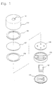
- As shown in Figs. 1 and 2, a conventional condenser microphone comprises a printed
circuit board 101, anFET 102 for converting the change of electric potential due to the variation of capacitance into an electrical signal, abase 103, apolar plate 104 on which a plurality of through holes are formed, aspacer 106, apolar ring 108, adiaphragm 107 being vibrated by the sound wave flowing therein, and acase 109 on which a soundwave inflow hole 110 is drilled. - The conventional condenser microphone is manufactured in such a manner that after the
polar ring 108, thediaphragm 107, thespacer 106 and thepolar plate 104 are sequentially assembled in thecase 109, and the printedcircuit board 101 on which the FET 102 is coupled is finally assembled therein, the one end of thecase 109 is folded. - In this case, the gate of the FET 102 is electrically connected to the
polar plate 104, and the source and drain thereof are exposed to the outside of the printedcircuit board 101. Before the printedcircuit board 101 is assembled in thecase 109, the source and drain of theFET 102 are folded downward to be inserted into the through holes of the printedcircuit board 101. Next, in order for the FET 102 to be temporarily secured on the printedcircuit board 101, the source and drain of the FET 102 are again folded to surround the printedcircuit board 101. Then, the gate of the FET 102 is folded upward such that upon assembling the FET 102 in thecase 109, it is connected to thepolar plate 104. Of course, the source and drain of the FET 102 should be folded back to the original state thereof after a manufacturing process. - In the conventional condenser microphone, however, since the source and drain of the
FET 102 are inserted into the through holes of the printedcircuit board 101 to be temporarily secured on the printedcircuit board 101 and then folded back, there arise some problems that the automation of the manufacturing process can not be realized and the source and drain of theFET 102 are likely to be disconnected due to the repetitive folding thereof. - Moreover, since the gate of the FET 102 and the
polar plate 104 are connected in a point contact, the connection there between is substantially unstable, and if there exists a slight gap between the FET 102 and thepolar plate 104, connection failure may be caused. - An embodiment of the invention provides a condenser microphone capable of realizing the automation of a manufacturing process by the connection of a FET to a printed circuit board by cream soldering and reducing the damage of the FET during the manufacturing process to improve production efficiency thereof.
- Another embodiment of the invention provides a condenser microphone capable of improving the connection method of a polar plate and a FET to prevent connection failure between the polar plate and the gate of the FET.
- According to the present invention, there is provided a condenser microphone constructed to convert the variation of capacitance between a diaphragm and a polar plate caused by sound wave into an electrical signal, which comprises: a printed circuit board having predetermined patterns formed on the both surfaces thereof and connected to each terminal of an FET; a metal ring for electrically connecting the gate of the FET and the polar plate; and a case electrically connected to a polar ring and for electrically connecting the diaphragm vibrated by the sound wave to the source of the FET.
- Preferably, the each terminal of the FET is connected to each pattern of the printed circuit board in such a manner that the gate thereof is folded and soldered to be connected to one of the patterns of the printed circuit board and the source and drain thereof are inserted to be passed through the printed circuit board and then soldered to be connected to ones of the patterns thereof.
- Preferably, the base ring of an insulation material should be interposed between the metal ring and the case, and a spacer of an insulation material should be interposed between the polar plate and the diaphragm so that the polar plate and the diaphragm are insulated and spaced out a predetermine distance apart from each other.
- An embodiment of the invention will now be described by way of example only with reference to the accompanying drawings, in which:
- Fig. 1 is a separated perspective view illustrating a conventional condenser microphone;
- Fig. 2 is a sectional view of Fig.1;
- Fig. 3 is a separated perspective view illustrating a condenser microphone according to the present invention;
- Fig. 4 is a sectional view of Fig. 3; and
- Figs. 5a and 5b are plan and bottom views illustrating the printed circuit board employed in the condenser microphone according to the present invention.
-
- In the various figures, like references refer to like parts.
- The condenser microphone according to the present invention is configured, as shown in Figs. 3 and 4, in such a manner that the gate of an
FET 2, which is connected to apattern 1G of a printedcircuit board 1, and the source and drain of the FET, which are inserted into the throughholes circuit board 1 are soldered by means of cream or soft solder, to thepattern - In this case, on the top surface of the printed
circuit board 1, as shown in Fig. 5a, thepredetermined patterns FET 2 and ametal ring 3, and as thepattern 1G connected to the gate of theFET 2 is the one which is electrically connected to the pattern connected to themetal ring 3, it is denoted by the same reference numeral. In the centers of thepatterns 1S, 1D, the throughholes circuit board 1 from top to bottom. And on the bottom surface of the printedcircuit board 1, as shown in Fig. 5b, thepattern 1S is formed to be electrically connected to the source of theFET 2, i.e. ground of theFET 2, as well as to thecase 9. - In other words, in process of connecting the
FET 2 to the printedcircuit board 1, after the source S and the drain D of theFET 2 are folded downward to be inserted into the throughholes pattern 1G, the each terminal G, D, S of theFET 2 is soldered to be electrically connected to eachpattern circuit board 1 by using a soft or cream solder. - On the printed
circuit board 1 on which the FET 2 is assembled, themetal ring 3 made of a conductive material, abase ring 3 of an insulation material, apolar plate 5 on which a plurality of holes are drilled, a spacer of an insulation material, adiaphragm 7 of a high molecular film and apolar ring 8 are electrically connected or built up to be insulated from each other. Acase 9 through which a soundwave inflow hole 10 is drilled is folded to surround the circumference of the printedcircuit board 1, while containing the components having thepolar ring 8. - In other words, the gate G of the
FET 2 is electrically connected to thepattern 1G of the printedcircuit board 1, themetal ring 3 and thepolar plate 5, and the source S thereof is electrically connected to the pattern IS of the printedcircuit board 1, thecase 9, thepolar ring 8 and thediaphragm 7. - Next, an explanation of an operation of the condenser microphone thus connected will be discussed.
- While the
diaphragm 7 is vibrated due to the sound wave flowing through the soundwave inflow hole 10, the interval between thediaphragm 7 and thepolar plate 5 is changed to thereby vary the capacitance there between. - Accordingly, as the electric potential of the
polar plate 5 is varied corresponding to the flowing of the sound wave and input to the gate G of theFET 2, the electric current flowing from the source S to the drain D of theFET 2 is amplified corresponding to the sound wave. - As a result, the condenser microphone can convert the flowing of the sound wave through the sound
wave inflow hole 10 into the electrical signal and amplify the converted electrical signal. - As discussed above, a condenser microphone according to the present invention is capable of realizing the automation of a manufacturing process and reducing the disconnection of the terminals of a FET during the manufacturing process as well by the connection of an FET to a printed circuit board by cream soldering.
- It will be apparent to those skilled in the art that various modifications and variations can be made in a condenser microphone of the present invention without departing from the spirit or scope of the invention. Thus, it is intended that the present invention cover the modifications and variations of this invention provided they come within the scope of the appended claims and their equivalents.
Claims (6)
- A condenser microphone for converting a variation of capacitance between a diaphragm and a polar plate caused by sound wave into an electrical signal, comprising:a printed circuit board having predetermined patterns formed on the both surfaces thereof and connected to each terminal of an FET;a metal ring for electrically connecting the gate of said FET and said polar plate; anda case electrically connected to a polar ring and for electrically connecting said diaphragm vibrated by the sound wave to the source of said FET.
- The condenser microphone according to claim 1, wherein each terminal of said FET is soldered to each of said predetermined patterns of said printed circuit board.
- The condenser microphone according to claim 1 or 2, wherein said gate of said FET is folded and soldered to be connected to one of said predetermined patterns of said printed circuit board.
- The condenser microphone according to claim 1 or 2, wherein said source and drain of said FET are inserted to be passed through said printed circuit board and then soldered to be connected to ones of said predetermined patterns of said printed circuit board.
- The condenser microphone according to claim 1, wherein a base ring of an insulation material is interposed between said metal ring and said case.
- The condenser microphone according to claim 1, wherein between said polar plate and said diaphragm, a spacer of an insulation material is interposed so that said polar plate and said diaphragm are insulated and spaced by a predetermined distance apart from each other.
Applications Claiming Priority (2)
| Application Number | Priority Date | Filing Date | Title |
|---|---|---|---|
| KR1019990055502A KR20000012476A (en) | 1999-12-07 | 1999-12-07 | Condenser microphone |
| KR9955502 | 1999-12-07 |
Publications (1)
| Publication Number | Publication Date |
|---|---|
| EP1107642A2 true EP1107642A2 (en) | 2001-06-13 |
Family
ID=19624020
Family Applications (1)
| Application Number | Title | Priority Date | Filing Date |
|---|---|---|---|
| EP00306107A Withdrawn EP1107642A2 (en) | 1999-12-07 | 2000-07-18 | Condenser microphone |
Country Status (4)
| Country | Link |
|---|---|
| EP (1) | EP1107642A2 (en) |
| JP (1) | JP2001186596A (en) |
| KR (1) | KR20000012476A (en) |
| CN (1) | CN1299228A (en) |
Cited By (2)
| Publication number | Priority date | Publication date | Assignee | Title |
|---|---|---|---|---|
| WO2005025269A1 (en) * | 2003-09-08 | 2005-03-17 | Sambu Communics Co., Ltd. | Condenser microphone |
| EP2271135A3 (en) * | 2009-07-03 | 2013-06-19 | Hosiden Corporation | Condenser microphone |
Families Citing this family (3)
| Publication number | Priority date | Publication date | Assignee | Title |
|---|---|---|---|---|
| KR100466403B1 (en) * | 2002-03-08 | 2005-01-13 | 주식회사 삼부커뮤닉스 | Condenser microphone |
| KR100508915B1 (en) * | 2002-10-10 | 2005-08-19 | 송기영 | structure and manufacturing methode of condenser microphone |
| CN1822721A (en) * | 2005-12-14 | 2006-08-23 | 潍坊歌尔电子有限公司 | Capacitance microphone |
-
1999
- 1999-12-07 KR KR1019990055502A patent/KR20000012476A/en not_active Ceased
-
2000
- 2000-07-18 EP EP00306107A patent/EP1107642A2/en not_active Withdrawn
- 2000-08-03 JP JP2000235447A patent/JP2001186596A/en active Pending
- 2000-08-03 CN CN00120928A patent/CN1299228A/en active Pending
Cited By (2)
| Publication number | Priority date | Publication date | Assignee | Title |
|---|---|---|---|---|
| WO2005025269A1 (en) * | 2003-09-08 | 2005-03-17 | Sambu Communics Co., Ltd. | Condenser microphone |
| EP2271135A3 (en) * | 2009-07-03 | 2013-06-19 | Hosiden Corporation | Condenser microphone |
Also Published As
| Publication number | Publication date |
|---|---|
| JP2001186596A (en) | 2001-07-06 |
| CN1299228A (en) | 2001-06-13 |
| KR20000012476A (en) | 2000-03-06 |
Similar Documents
| Publication | Publication Date | Title |
|---|---|---|
| JP3355353B2 (en) | Electrical connector | |
| JP3194225B2 (en) | Card edge electrical connector with terminals with improved solder tail | |
| JP3111383B2 (en) | Card edge connector | |
| US3775572A (en) | Condenser microphone | |
| KR100341564B1 (en) | Condenser microphone | |
| JP2003153392A (en) | Electret capacitor microphone | |
| KR20010007704A (en) | method for manufacturing of condenser microphone | |
| EP1107642A2 (en) | Condenser microphone | |
| US20050069158A1 (en) | Packaged piezoelectric exciter module | |
| AU2003209622A1 (en) | Pixel sensor array and method of manufacture thereof | |
| AU632834B2 (en) | Connector assembly for electronic devices | |
| KR20010074030A (en) | Method for manufacturing of condenser microphone | |
| KR100406256B1 (en) | Microphone including printed circuit board having protrusion portion for electrical contact and Method of connecting for it to outer apparatus | |
| KR100644991B1 (en) | Surface-Mount Electret Condenser Microphone and Manufacturing Method Thereof | |
| KR100331020B1 (en) | terminal of flexible printed circuit and method there of | |
| KR20040079776A (en) | Electret condenser microphone | |
| KR100466403B1 (en) | Condenser microphone | |
| KR200282644Y1 (en) | Condenser microphone for surface mounting technique | |
| JPH09274949A (en) | Connector for circuit board and method of mounting the connector on circuit board | |
| JP2001015881A (en) | Electronic circuit unit | |
| KR200310591Y1 (en) | A structure of pcb for condenser microphone | |
| JPS6325839Y2 (en) | ||
| KR200340623Y1 (en) | Conductive stub of a sound exciter | |
| JP2534049Y2 (en) | Dielectric filter | |
| JPH08148908A (en) | Irreversible circuit element |
Legal Events
| Date | Code | Title | Description |
|---|---|---|---|
| PUAI | Public reference made under article 153(3) epc to a published international application that has entered the european phase |
Free format text: ORIGINAL CODE: 0009012 |
|
| AK | Designated contracting states |
Kind code of ref document: A2 Designated state(s): AT BE CH CY DE DK ES FI FR GB GR IE IT LI LU MC NL PT SE |
|
| AX | Request for extension of the european patent |
Free format text: AL;LT;LV;MK;RO;SI |
|
| STAA | Information on the status of an ep patent application or granted ep patent |
Free format text: STATUS: THE APPLICATION IS DEEMED TO BE WITHDRAWN |
|
| 18D | Application deemed to be withdrawn |
Effective date: 20030203 |