EP1107485A2 - Device for transmitting and receiving optical signals - Google Patents
Device for transmitting and receiving optical signals Download PDFInfo
- Publication number
- EP1107485A2 EP1107485A2 EP00125325A EP00125325A EP1107485A2 EP 1107485 A2 EP1107485 A2 EP 1107485A2 EP 00125325 A EP00125325 A EP 00125325A EP 00125325 A EP00125325 A EP 00125325A EP 1107485 A2 EP1107485 A2 EP 1107485A2
- Authority
- EP
- European Patent Office
- Prior art keywords
- signal
- light
- electric signal
- set forth
- optical
- Prior art date
- Legal status (The legal status is an assumption and is not a legal conclusion. Google has not performed a legal analysis and makes no representation as to the accuracy of the status listed.)
- Withdrawn
Links
- 230000003287 optical effect Effects 0.000 title claims abstract description 105
- 230000001427 coherent effect Effects 0.000 claims abstract description 46
- 239000013307 optical fiber Substances 0.000 claims abstract description 14
- 238000000034 method Methods 0.000 claims description 7
- 230000003111 delayed effect Effects 0.000 claims description 3
- 238000010586 diagram Methods 0.000 description 6
- 206010034972 Photosensitivity reaction Diseases 0.000 description 5
- 230000036211 photosensitivity Effects 0.000 description 5
- 230000006866 deterioration Effects 0.000 description 4
- 239000004065 semiconductor Substances 0.000 description 3
- 230000005540 biological transmission Effects 0.000 description 2
- 230000015572 biosynthetic process Effects 0.000 description 1
- 230000002452 interceptive effect Effects 0.000 description 1
- 239000000758 substrate Substances 0.000 description 1
Images




Classifications
-
- H—ELECTRICITY
- H04—ELECTRIC COMMUNICATION TECHNIQUE
- H04B—TRANSMISSION
- H04B10/00—Transmission systems employing electromagnetic waves other than radio-waves, e.g. infrared, visible or ultraviolet light, or employing corpuscular radiation, e.g. quantum communication
- H04B10/60—Receivers
Definitions
- the invention relates to an asynchronous transfer mode-passive optical network (ATM-PON) system, more particularly to a device for transmitting and receiving optical signals used in an ATM-PON system, and most particularly to removal of a coherent light in such a device.
- ATM-PON asynchronous transfer mode-passive optical network
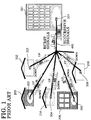
- Fig. 1 illustrates an ATM-PON system.
- optical signals are interactively transmitted between a station 201 and subscribers 202 to 206.
- the station 201 is connected to each of the subscribers 202 to 206 through one-core optical fibers 400.
- optical signals successively transmitted from the station 201 to the subscribers 202 to 206 are called down signals, and burst signals transmitted from each of the subscribers 202 to 206 to the station 201 is called up signals.
- the up and down signals are designed to have different wavelengths from each other.
- Devices 301 to 306 equipped in the station 201 and each of the subscribers 202 to 206 are designed to be able to not only transmit an optical signal, but also receive an optical signal.
- Each of the devices 301 to 306 is designed to include a laser diode (LD) from which an optical signal is transmitted.
- LD laser diode
- Fig. 2 is a circuit diagram of a circuit included in each of the devices 301 to 306 for receiving optical signals.
- the illustrated circuit is comprised of a photodiode 101, a trans-impedance amplifier 102 electrically connected in series to the photodiode 101. and a feedback resistor 103 electrically connected in parallel to the trans-impedance amplifier 102.
- the photodiode 101 converts a received optical signal into an electric signal.
- the trans-impedance amplifier 102 amplifies and converts the electric signal transmitted from the photodiode 101, into a voltage signal.
- the feedback resistor 103 defines a gain of the trans-impedance amplifier 102.
- the above-mentioned devices 301 to 306 are accompanied with a problem that when the laser diode transmits an optical signal, the optical signal to be transmitted strays in the devices 301 to 306, and enters the circuit illustrated in Fig. 2 as a coherent light, resulting in deterioration in photosensitivity in the devices 301 to 306.
- the above-mentioned coherent light exerts much harmful influence on the circuit illustrated in Fig 2, resulting in more remarkable deterioration in photosensitivity in the devices 301 to 306.
- optical countermeasure In order to remove a coherent light component from a received optical signal, optical countermeasure has been conventionally applied to an optical waveguide.
- Japanese Unexamined Patent Publication No. 10-54917 has suggested the formation of a slit in an optical waveguide for interrupting a coherent light from reaching the optical waveguide.
- Japanese Unexamined Patent Publication No. 5-289120 has suggested an optical waveguide device including a device for combining optical signals to one another and separating optical signals into respective optical signals. an optical directional coupler, and an optical circuit substrate on which the device and the optical directional coupler are formed in monolithic.
- Japanese Patent No. 2923884 Japanese Unexamined Patent Publication No. 10-311875 has suggested a device including a semiconductor laser emitting a laser beam, a laser receiver receiving the laser beam emitted from the semiconductor laser, a filter positioned between the laser receiver and the semiconductor laser and allowing the laser beam to pass therethrough, the filter removing background noises. an angle adjuster adjusting an inclination angle of the filter to change an incident angle of the laser beam into the filter, and a controller controlling the angle adjuster such that the laser beam passes through the filter at a maximum, in accordance with an output signal transmitted from the laser receiver.
- the controller includes an oscillator, a multiplier multiplying an output of the oscillator by an output of the laser receiver, a differential amplifier amplifying a difference between an output of the multiplier and a reference voltage, and a manipulator overlapping an output of the differential amplifier with an output of the oscillator, and providing a command to the angle adjuster.
- Japanese Unexamined Patent Publication No. 11-27215 has suggested an optical communication module to be used in a parent station radially connected to a plurality of child stations through optical devices and making interactive communication with each of the child stations in time division multiplex by switching a mode between a receipt mode and a transmission mode.
- the parent station includes first output means for transmitting a first reset signal in accordance with a difference in a signal receiving level in the receipt mode, second output means for transmitting a second reset signal when the transmission mode is switched to the receipt mode. and ATC means for automatically setting a threshold level when the first or second reset signal is received.
- a device for interactively transmitting optical signals in a first wavelength and receiving optical signals in a second wavelength both through a one-core optical fiber characterized by (a) a first light-electricity signal converter which converts a received optical signal into a first electric signal, (b) a second light-electricity signal converter which converts an optical signal to be transmitted, into a second electric signal, and (c) a coherent light remover which subtracts a level of the second electric signal from a level of the first electric signal to remove a coherent light included in the received optical signal.
- a method of removing a coherent light in a device for interactively transmitting optical signals in a first wavelength and receiving optical signals in a second wavelength both through a one-core optical fiber including the steps of (a) converting a received optical signal into a first electric signal, (b) converting an optical signal to be transmitted, into a second electric signal, and (c) subtracting a level of the second electric signal from a level of the first electric signal to remove a coherent light included in the received optical signal.
- the device including an optical waveguide it is quite important for the device including an optical waveguide to prevent deterioration in photosensitivity, caused by a coherent light. Since the present invention removes a coherent light by a simply structured circuit, this is quite effective for the device including an optical waveguide.
- Fig. 1 illustrates an asynchronous transfer mode-passive optical network (ATM-PON) system.
- ATM-PON asynchronous transfer mode-passive optical network
- Fig. 2 is a circuit diagram of a circuit for receiving an optical signal, equipped in a conventional device for transmitting and receiving optical signals.
- Fig. 3 is a device for transmitting and receiving optical signals, including an optical waveguide, in accordance with an embodiment of the present invention.
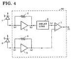
- Fig. 4 is a block diagram of a circuit for removing a coherent light, to be applied to the device illustrated in Fig. 3.
- Fig. 5 is a timing chart showing an operation of the circuit illustrated in Fig. 4.
- Fig. 6 is another block diagram of a circuit for removing a coherent light, to be applied to the device illustrated in Fig. 3.
- Fig. 3 illustrates a device for transmitting and receiving optical signals, including an optical waveguide, in accordance with the embodiment.
- the device illustrated in Fig. 3 is equipped in the station 201 and each of the subscribers 202 to 206 in the ATM-PON system illustrated in Fig. 1.
- the device includes an optical waveguide element 10 in which an optical waveguide 11 is arranged, a filter 12 for selecting a wavelength, a first photodiode (PD) 1, a laser diode (LD) 9. and a second photodiode 4.
- the optical waveguide 11 is connected to a one-core optical fiber 400.
- An optical signal having a first wavelength is transmitted to the optical waveguide 11 through the one-core optical fiber 400, and an optical signal having a second wavelength is received at the optical waveguide 11 through the one-core optical fiber 400.
- An optical signal received through the one-core optical fiber 400 is introduced into the optical waveguide 11 at one of input ports of the optical waveguide 11.
- the received optical signal introduced into the optical waveguide 11 passes through the filter 12 and is received at the first photodiode 1.
- the optical signal having been emitted from the laser diode 9 and introduced into the optical waveguide 11 is reflected at the filter 12, advances through the optical waveguide 11, and is connected to and output from the one-core optical fiber 400.
- optical signals emitted from the laser diode 9 When the optical signals emitted from the laser diode 9 are introduced into the optical waveguide 11, some of the optical signals cannot be connected to the optical waveguide 11. Such optical signals scatter in the optical waveguide element 10, and are received at the photodiode 1 together with a received optical signal as a coherent light against the received optical signal.
- the second photodiode 4 is located at the rear of the laser diode 9 to receive a backlight emitted from the laser diode 9.
- the backlight emitted from the laser diode 9 and received at the second photodiode 4 has the same waveform as that of an optical signal to be output from the device. Since a coherent light included in the received optical signal consists of a light emitted from the laser diode 9, it is possible to detect only a coherent light by means of the second photodiode 4.
- Fig. 4 is a block diagram of a circuit 20 for removing a coherent light. This circuit is applied to the device in accordance with the embodiment.
- the illustrated circuit 20 is comprised of a first trans-impedance amplifier 2 electrically connected in series to the first photodiode 1, a first feedback resistor 3 electrically connected in parallel to the first trans-impedance amplifier 2, a second trans-impedance amplifier 5 electrically connected in series to the second photodiode 4, a second feedback resistor 6 electrically connected in parallel to the second trans-impedance amplifier 5, a differential amplifier 7 receiving output signals transmitted from the first and second trans-impedance amplifiers 2 and 5, and a delay line 8 electrically connected between the first trans-impedance amplifier 2 and the differential amplifier 7.
- the first photodiode 1 converts a received optical signal into a first electric signal, which is in turn introduced into the first trans-impedance amplifier 2.
- the first trans-impedance amplifier 2 converts the thus received first electric signal into a first voltage signal.
- a resistance of the first feedback resistor 3 defines a gain of the first trans-impedance amplifier 2 at which the first trans-impedance amplifier 2 converts an electric signal into a voltage signal.
- the second photodiode 4 receives only a coherent light, as mentioned earlier, and converts the received coherent light into a second electric signal.
- the second electric signal is introduced into the second trans-impedance amplifier 5, which converts the second electric signal into a second voltage signal.
- a resistance of the second feedback resistor 6 defines a gain of the second trans-impedance amplifier 5 at which the second trans-impedance amplifier 5 converts an electric signal into a voltage signal.
- the first voltage signal transmitted from the first trans-impedance amplifier 2 is introduced into the delay line 8.
- the delay line 8 adjusts a phase difference between the optical signal received at the first photodiode 1 and the optical signal received at the second photodiode 4.
- An output signal transmitted from the delay line 8 and the second voltage signal transmitted from the second trans-impedance amplifier 5 are both introduced into the differential amplifier 7.
- the differential amplifier 7 subtracts a level of the second electric signal from a level of the first electric signal, and transmits an output signal indicative of the result.
- the delay line 8 is positioned between the first trans-impedance amplifier 2 and the differential amplifier 7 in the circuit 20 illustrated in Fig. 4, where the delay line 8 should be positioned is determined in dependence on a structure of the device and other conditions.
- the delay line 8 is positioned between the second trans-impedance amplifier 5 and the differential amplifier 7.
- the delay line 8 is positioned between the first trans-impedance amplifier 2 and the differential amplifier 7, as shown in Fig. 4.
- the second photodiode 4 receives only a backlight from the laser diode 9, that is, a coherent light. Hence, it is possible to detect and remove a coherent light component by subtracting the second electric signal level from the first electric signal level by means of the differential amplifier 7.
- Fig. 5 is a timing chart showing an operation of the circuit 20 illustrated in Fig. 4.
- Fig. 5-(a) illustrates a signal waveform of the first electric signal transmitted from the first photodiode 1. Since the signal received at the first photodiode 1 includes a coherent light emitted from the laser diode 9, the signal waveform in Fig. 5-(a) is deformed.
- Fig. 5-(b) illustrates a signal waveform of the first voltage signal transmitted from the first trans-impedance amplifier 2.
- the gain at which the first electric signal is converted into the first voltage signal is defined by the first feedback resistor 3.
- Fig. 5-(c) illustrates a signal waveform of the signal transmitted from the delay line 8. As illustrated in Fig. 5-(c), a phase of the first voltage signal illustrated in Fig. 5-(b) is delayed such that the first voltage signal is in phase with the second voltage signal illustrated in Fig. 5-(e).
- Fig. 5-(d) illustrates a signal waveform of the second electric signal transmitted from the second photodiode 4.
- This signal waveform is a signal waveform of a light transmitted from the laser diode 9. that is, a coherent light.
- Fig. 5-(e) illustrates a signal waveform of the second voltage signal transmitted from the second trans-impedance amplifier 5.
- the gain at which the second electric signal is converted into the second voltage signal is defined by the second feedback resistor 6 such that a level of the signal transmitted from the delay line 8, illustrated in Fig. 5-(c), is equal to a level of the second voltage signal transmitted from the second trans-impedance amplifier 5, including a coherent light, illustrated in Fig. 5-(e).
- a delay in a phase brought by the delay line 8 is determined such that the signal illustrated in Fig. 5-(c) is in phase with the signal illustrated in Fig. 5-(e).
- Fig. 5-(f) illustrates a signal waveform of the signal transmitted from the differential amplifier 7.
- Fig. 6 is a block diagram of a circuit 30 for removing a coherent light. This circuit 30 is applied to the device in accordance with the embodiment.
- the illustrated circuit 30 is comprised of a first trans-impedance amplifier 2 electrically connected in series to the first photodiode 1, a first feedback resistor 3 electrically connected in parallel to the first trans-impedance amplifier 2, a second trans-impedance amplifier 5 electrically connected in series to the second photodiode 4, a second variable feedback resistor 6 electrically connected in parallel to the second trans-impedance amplifier 5, a differential amplifier 7 receiving output signals transmitted from the first and second trans-impedance amplifiers 2 and 5, a delay line 8 electrically connected between the first trans-impedance amplifier 2 and the differential amplifier 7, a third trans-impedance amplifier 14 electrically connected in series to the second photodiode 4, and a third variable feedback resistor 15 electrically connected in parallel to the third trans-impedance amplifier 14.
- circuit 30 illustrated in Fig. 6 further includes the third trans-impedance amplifier 14 and the third variable feedback resistor 15 in comparison with the circuit 20 illustrated in Fig. 4.
- the third trans-impedance amplifier 14 transmits an output signal, for instance, to a circuit (not illustrated) for detecting whether an optical output is interrupted.
- the second photodiode 4 can act also as such a monitor photodiode. That is, it is possible to apply the circuit 30 to a circuit having to include a monitor photodiode, without newly adding a photodiode to the circuit.
- circuit 30 It is of course possible for the circuit 30 to detect whether an optical output is interrupted, without adding a photodiode thereto.
Landscapes
- Physics & Mathematics (AREA)
- Electromagnetism (AREA)
- Engineering & Computer Science (AREA)
- Computer Networks & Wireless Communication (AREA)
- Signal Processing (AREA)
- Optical Communication System (AREA)
- Cable Transmission Systems, Equalization Of Radio And Reduction Of Echo (AREA)
Abstract
A device for interactively transmitting optical signals in a first
wavelength and receiving optical signals in a second wavelength both through a
one-core optical fiber (400), is characterized by a first light-electricity signal
converter (1) which converts a received optical signal into a first electric signal, a
second light-electricity signal converter (4) which converts an optical signal to be
transmitted, into a second electric signal, a delay line (8) which adjusts a phase
difference between the first and second electric signals such that the first and
second electric signals are in phase with each other, and a coherent light remover
(7) which subtracts a level of the second electric signal from a level of the first
electric signal to remove a coherent light included in the received optical signal.
Description
- The invention relates to an asynchronous transfer mode-passive optical network (ATM-PON) system, more particularly to a device for transmitting and receiving optical signals used in an ATM-PON system, and most particularly to removal of a coherent light in such a device.
- Fig. 1 illustrates an ATM-PON system. In the ATM-PON system, optical signals are interactively transmitted between a
station 201 andsubscribers 202 to 206. Thestation 201 is connected to each of thesubscribers 202 to 206 through one-coreoptical fibers 400. - Herein, optical signals successively transmitted from the
station 201 to thesubscribers 202 to 206 are called down signals, and burst signals transmitted from each of thesubscribers 202 to 206 to thestation 201 is called up signals. The up and down signals are designed to have different wavelengths from each other. -
Devices 301 to 306 equipped in thestation 201 and each of thesubscribers 202 to 206 are designed to be able to not only transmit an optical signal, but also receive an optical signal. - Each of the
devices 301 to 306 is designed to include a laser diode (LD) from which an optical signal is transmitted. - Fig. 2 is a circuit diagram of a circuit included in each of the
devices 301 to 306 for receiving optical signals. The illustrated circuit is comprised of aphotodiode 101, a trans-impedance amplifier 102 electrically connected in series to thephotodiode 101. and afeedback resistor 103 electrically connected in parallel to the trans-impedance amplifier 102. - The
photodiode 101 converts a received optical signal into an electric signal. The trans-impedance amplifier 102 amplifies and converts the electric signal transmitted from thephotodiode 101, into a voltage signal. Thefeedback resistor 103 defines a gain of the trans-impedance amplifier 102. - The above-mentioned
devices 301 to 306 are accompanied with a problem that when the laser diode transmits an optical signal, the optical signal to be transmitted strays in thedevices 301 to 306, and enters the circuit illustrated in Fig. 2 as a coherent light, resulting in deterioration in photosensitivity in thedevices 301 to 306. - When the
devices 301 to 306 are of an optical waveguide, in particular, the above-mentioned coherent light exerts much harmful influence on the circuit illustrated in Fig 2, resulting in more remarkable deterioration in photosensitivity in thedevices 301 to 306. - In order to minimize deterioration in photosensitivity in the
devices 301 to 306 in their operation, it is necessary to remove a coherent light component from a received optical signal. - In order to remove a coherent light component from a received optical signal, optical countermeasure has been conventionally applied to an optical waveguide. For instance, Japanese Unexamined Patent Publication No. 10-54917 has suggested the formation of a slit in an optical waveguide for interrupting a coherent light from reaching the optical waveguide.
- However, it was quite difficult or almost impossible to sufficiently remove a coherent light only by means of optical countermeasures.
- Japanese Unexamined Patent Publication No. 5-289120 has suggested an optical waveguide device including a device for combining optical signals to one another and separating optical signals into respective optical signals. an optical directional coupler, and an optical circuit substrate on which the device and the optical directional coupler are formed in monolithic.
- Japanese Patent No. 2923884 (Japanese Unexamined Patent Publication No. 10-311875) has suggested a device including a semiconductor laser emitting a laser beam, a laser receiver receiving the laser beam emitted from the semiconductor laser, a filter positioned between the laser receiver and the semiconductor laser and allowing the laser beam to pass therethrough, the filter removing background noises. an angle adjuster adjusting an inclination angle of the filter to change an incident angle of the laser beam into the filter, and a controller controlling the angle adjuster such that the laser beam passes through the filter at a maximum, in accordance with an output signal transmitted from the laser receiver. The controller includes an oscillator, a multiplier multiplying an output of the oscillator by an output of the laser receiver, a differential amplifier amplifying a difference between an output of the multiplier and a reference voltage, and a manipulator overlapping an output of the differential amplifier with an output of the oscillator, and providing a command to the angle adjuster.
- Japanese Unexamined Patent Publication No. 11-27215 has suggested an optical communication module to be used in a parent station radially connected to a plurality of child stations through optical devices and making interactive communication with each of the child stations in time division multiplex by switching a mode between a receipt mode and a transmission mode. The parent station includes first output means for transmitting a first reset signal in accordance with a difference in a signal receiving level in the receipt mode, second output means for transmitting a second reset signal when the transmission mode is switched to the receipt mode. and ATC means for automatically setting a threshold level when the first or second reset signal is received.
- In view of the above-mentioned problem in the prior art, it is an object of the present invention to provide a device for interactively transmitting optical signals and receiving optical, which is capable of removing a coherent light by which photosensitivity in the device would be deteriorated.
- In one aspect of the present invention, there is provided a device for interactively transmitting optical signals in a first wavelength and receiving optical signals in a second wavelength both through a one-core optical fiber, characterized by (a) a first light-electricity signal converter which converts a received optical signal into a first electric signal, (b) a second light-electricity signal converter which converts an optical signal to be transmitted, into a second electric signal, and (c) a coherent light remover which subtracts a level of the second electric signal from a level of the first electric signal to remove a coherent light included in the received optical signal.
- In another aspect of the present invention, there is provided a method of removing a coherent light in a device for interactively transmitting optical signals in a first wavelength and receiving optical signals in a second wavelength both through a one-core optical fiber, including the steps of (a) converting a received optical signal into a first electric signal, (b) converting an optical signal to be transmitted, into a second electric signal, and (c) subtracting a level of the second electric signal from a level of the first electric signal to remove a coherent light included in the received optical signal.
- The advantages obtained by the aforementioned present invention will be described hereinbelow.
- In accordance with the above-mentioned present invention, only a coherent light included a received optical signal is detected and remove. Accordingly, it is possible to electrically remove a coherent light without applying an optical countermeasure to the device.
- In particular. it is quite important for the device including an optical waveguide to prevent deterioration in photosensitivity, caused by a coherent light. Since the present invention removes a coherent light by a simply structured circuit, this is quite effective for the device including an optical waveguide.
- Fig. 1 illustrates an asynchronous transfer mode-passive optical network (ATM-PON) system.
- Fig. 2 is a circuit diagram of a circuit for receiving an optical signal, equipped in a conventional device for transmitting and receiving optical signals.
- Fig. 3 is a device for transmitting and receiving optical signals, including an optical waveguide, in accordance with an embodiment of the present invention.
- Fig. 4 is a block diagram of a circuit for removing a coherent light, to be applied to the device illustrated in Fig. 3.
- Fig. 5 is a timing chart showing an operation of the circuit illustrated in Fig. 4.
- Fig. 6 is another block diagram of a circuit for removing a coherent light, to be applied to the device illustrated in Fig. 3.
- Preferred embodiments in accordance with the present invention will be explained hereinbelow with reference to drawings.
- Fig. 3 illustrates a device for transmitting and receiving optical signals, including an optical waveguide, in accordance with the embodiment.
- The device illustrated in Fig. 3 is equipped in the
station 201 and each of thesubscribers 202 to 206 in the ATM-PON system illustrated in Fig. 1. The device includes anoptical waveguide element 10 in which anoptical waveguide 11 is arranged, afilter 12 for selecting a wavelength, a first photodiode (PD) 1, a laser diode (LD) 9. and asecond photodiode 4. Theoptical waveguide 11 is connected to a one-coreoptical fiber 400. - An optical signal having a first wavelength is transmitted to the
optical waveguide 11 through the one-coreoptical fiber 400, and an optical signal having a second wavelength is received at theoptical waveguide 11 through the one-coreoptical fiber 400. - An optical signal received through the one-core
optical fiber 400 is introduced into theoptical waveguide 11 at one of input ports of theoptical waveguide 11. - The received optical signal introduced into the
optical waveguide 11 passes through thefilter 12 and is received at thefirst photodiode 1. - A laser beam emitted from the
laser diode 9, which is to be transmitted from the device through the one-coreoptical fiber 400, is introduced into theoptical waveguide 11 at the other input port of theoptical waveguide 11. - The optical signal having been emitted from the
laser diode 9 and introduced into theoptical waveguide 11 is reflected at thefilter 12, advances through theoptical waveguide 11, and is connected to and output from the one-coreoptical fiber 400. - When the optical signals emitted from the
laser diode 9 are introduced into theoptical waveguide 11, some of the optical signals cannot be connected to theoptical waveguide 11. Such optical signals scatter in theoptical waveguide element 10, and are received at thephotodiode 1 together with a received optical signal as a coherent light against the received optical signal. - The
second photodiode 4 is located at the rear of thelaser diode 9 to receive a backlight emitted from thelaser diode 9. - The backlight emitted from the
laser diode 9 and received at thesecond photodiode 4 has the same waveform as that of an optical signal to be output from the device. Since a coherent light included in the received optical signal consists of a light emitted from thelaser diode 9, it is possible to detect only a coherent light by means of thesecond photodiode 4. - Fig. 4 is a block diagram of a
circuit 20 for removing a coherent light. This circuit is applied to the device in accordance with the embodiment. - The illustrated
circuit 20 is comprised of a first trans-impedance amplifier 2 electrically connected in series to thefirst photodiode 1, afirst feedback resistor 3 electrically connected in parallel to the first trans-impedance amplifier 2, a second trans-impedance amplifier 5 electrically connected in series to thesecond photodiode 4, asecond feedback resistor 6 electrically connected in parallel to the second trans-impedance amplifier 5, adifferential amplifier 7 receiving output signals transmitted from the first and second trans-impedance amplifiers delay line 8 electrically connected between the first trans-impedance amplifier 2 and thedifferential amplifier 7. - The
first photodiode 1 converts a received optical signal into a first electric signal, which is in turn introduced into the first trans-impedance amplifier 2. - The first trans-
impedance amplifier 2 converts the thus received first electric signal into a first voltage signal. A resistance of thefirst feedback resistor 3 defines a gain of the first trans-impedance amplifier 2 at which the first trans-impedance amplifier 2 converts an electric signal into a voltage signal. - The
second photodiode 4 receives only a coherent light, as mentioned earlier, and converts the received coherent light into a second electric signal. The second electric signal is introduced into the second trans-impedance amplifier 5, which converts the second electric signal into a second voltage signal. A resistance of thesecond feedback resistor 6 defines a gain of the second trans-impedance amplifier 5 at which the second trans-impedance amplifier 5 converts an electric signal into a voltage signal. - The first voltage signal transmitted from the first trans-
impedance amplifier 2 is introduced into thedelay line 8. Thedelay line 8 adjusts a phase difference between the optical signal received at thefirst photodiode 1 and the optical signal received at thesecond photodiode 4. - An output signal transmitted from the
delay line 8 and the second voltage signal transmitted from the second trans-impedance amplifier 5 are both introduced into thedifferential amplifier 7. Thedifferential amplifier 7 subtracts a level of the second electric signal from a level of the first electric signal, and transmits an output signal indicative of the result. - Though the
delay line 8 is positioned between the first trans-impedance amplifier 2 and thedifferential amplifier 7 in thecircuit 20 illustrated in Fig. 4, where thedelay line 8 should be positioned is determined in dependence on a structure of the device and other conditions. - For instance, if a signal received at the
second photodiode 4 reaches thedifferential amplifier 7 earlier than a signal received at thefirst photodiode 1, thedelay line 8 is positioned between the second trans-impedance amplifier 5 and thedifferential amplifier 7. - In contrast, if a signal received at the
first photodiode 1 reaches thedifferential amplifier 7 earlier than a signal received at thesecond photodiode 4, thedelay line 8 is positioned between the first trans-impedance amplifier 2 and thedifferential amplifier 7, as shown in Fig. 4. - As mentioned above, the
second photodiode 4 receives only a backlight from thelaser diode 9, that is, a coherent light. Hence, it is possible to detect and remove a coherent light component by subtracting the second electric signal level from the first electric signal level by means of thedifferential amplifier 7. - Fig. 5 is a timing chart showing an operation of the
circuit 20 illustrated in Fig. 4. - Fig. 5-(a) illustrates a signal waveform of the first electric signal transmitted from the
first photodiode 1. Since the signal received at thefirst photodiode 1 includes a coherent light emitted from thelaser diode 9, the signal waveform in Fig. 5-(a) is deformed. - Fig. 5-(b) illustrates a signal waveform of the first voltage signal transmitted from the first trans-
impedance amplifier 2. The gain at which the first electric signal is converted into the first voltage signal is defined by thefirst feedback resistor 3. - Fig. 5-(c) illustrates a signal waveform of the signal transmitted from the
delay line 8. As illustrated in Fig. 5-(c), a phase of the first voltage signal illustrated in Fig. 5-(b) is delayed such that the first voltage signal is in phase with the second voltage signal illustrated in Fig. 5-(e). - Fig. 5-(d) illustrates a signal waveform of the second electric signal transmitted from the
second photodiode 4. This signal waveform is a signal waveform of a light transmitted from thelaser diode 9. that is, a coherent light. - Fig. 5-(e) illustrates a signal waveform of the second voltage signal transmitted from the second trans-
impedance amplifier 5. The gain at which the second electric signal is converted into the second voltage signal is defined by thesecond feedback resistor 6 such that a level of the signal transmitted from thedelay line 8, illustrated in Fig. 5-(c), is equal to a level of the second voltage signal transmitted from the second trans-impedance amplifier 5, including a coherent light, illustrated in Fig. 5-(e). - A delay in a phase brought by the
delay line 8 is determined such that the signal illustrated in Fig. 5-(c) is in phase with the signal illustrated in Fig. 5-(e). - Fig. 5-(f) illustrates a signal waveform of the signal transmitted from the
differential amplifier 7. - By subtracting the signal waveform illustrated in Fig. 5-(e) from the signal waveform illustrated in Fig. 5-(c), it is possible to obtain a signal waveform including no coherent light.
- Fig. 6 is a block diagram of a
circuit 30 for removing a coherent light. Thiscircuit 30 is applied to the device in accordance with the embodiment. - The illustrated
circuit 30 is comprised of a first trans-impedance amplifier 2 electrically connected in series to thefirst photodiode 1, afirst feedback resistor 3 electrically connected in parallel to the first trans-impedance amplifier 2, a second trans-impedance amplifier 5 electrically connected in series to thesecond photodiode 4, a secondvariable feedback resistor 6 electrically connected in parallel to the second trans-impedance amplifier 5, adifferential amplifier 7 receiving output signals transmitted from the first and second trans-impedance amplifiers delay line 8 electrically connected between the first trans-impedance amplifier 2 and thedifferential amplifier 7, a third trans-impedance amplifier 14 electrically connected in series to thesecond photodiode 4, and a thirdvariable feedback resistor 15 electrically connected in parallel to the third trans-impedance amplifier 14. - In brief, the
circuit 30 illustrated in Fig. 6 further includes the third trans-impedance amplifier 14 and the thirdvariable feedback resistor 15 in comparison with thecircuit 20 illustrated in Fig. 4. - The third trans-
impedance amplifier 14 transmits an output signal, for instance, to a circuit (not illustrated) for detecting whether an optical output is interrupted. - If a monitor photodiode is to be used for detecting whether an optical output is interrupted, the
second photodiode 4 can act also as such a monitor photodiode. That is, it is possible to apply thecircuit 30 to a circuit having to include a monitor photodiode, without newly adding a photodiode to the circuit. - It is of course possible for the
circuit 30 to detect whether an optical output is interrupted, without adding a photodiode thereto.
Claims (19)
- A device for interactively transmitting optical signals in a first wavelength and receiving optical signals in a second wavelength both through a one-core optical fiber (400),
characterized by(a) a first light-electricity signal converter (1) which converts a received optical signal into a first electric signal;(b) a second light-electricity signal converter (4) which converts an optical signal to be transmitted, into a second electric signal; and(c) a coherent light remover (7) which subtracts a level of the second electric signal from a level of the first electric signal to remove a coherent light included in the received optical signal. - The device as set forth in claim 1, further comprising a delay line (8) which adjusts a phase difference between the first and second electric signals such that the first and second electric signals are in phase with each other.
- The device as set forth in claim 2, wherein the delay line (8) is positioned between the first light-electricity signal converter (1) and the coherent light remover (7) when the first electric signal reaches the coherent light remover (7) earlier than the second electric signal.
- The device as set forth in claim 2, wherein the delay line (8) is positioned between the second light-electricity signal converter (4) and the coherent light remover (7) when the second electric signal reaches the coherent light remover (7) earlier than the first electric signal.
- The device as set forth in any of claims 1 to 4, further comprising a first variable gain amplifier (2, 3) electrically connected in series between the first light-electricity signal converter (1) and the coherent light remover (7).
- The device as set forth in claim 5, wherein the first variable gain amplifier is comprised of a first impedance amplifier (2) electrically connected in series to the first light-electricity signal converter (1), and a first variable resistor (3) electrically connected in parallel to the first impedance amplifier (2).
- The device as set forth in any of claims 1 to 6, further comprising a second variable gain amplifier (5, 6) electrically connected in series between the second light-electricity signal converter (4) and the coherent light remover (7), the second variable gain amplifier equalizing a level of an output signal transmitted from the second light-electricity signal converter (4), to a signal level of a coherent light included in the received optical signal.
- The device as set forth in claim 7, wherein the second variable gain amplifier is comprised of a second impedance amplifier (5) electrically connected in series to the second light-electricity signal converter (4), and a second variable resistor (6) electrically connected in parallel to the second impedance amplifier (5).
- The device as set forth in claim 7 or 8, further comprising a third variable gain amplifier (14, 15) electrically connected in series to the second light-electricity signal converter (4), and in parallel with the second variable gain amplifier (5, 6).
- The device as set forth in claim 9. wherein the third variable gain amplifier is comprised of a third impedance amplifier (14) electrically connected in series to the second light-electricity signal converter (4), and a third variable resistor (15) electrically connected in parallel to the third impedance amplifier (14).
- The device as set forth in any of claims 1 to 10, wherein the device is of a waveguide type.
- The device as set forth in any of claims 1 to 11, wherein the first light-electricity signal converter (1) is comprised of a first photodiode, the second light-electricity signal converter (4) is comprised of a second photodiode, and the coherent light remover (7) is comprised of a differential amplifier.
- The device as set forth in any one of claims 1-4, 6 and 8-10, further comprising:the second light-electricity signal converter (4) being located at the rear of the laser diode (9) and receiving a backlight from the second light-electricity signal converter (4).(d) an optical waveguide (11) connected to the one-core optical fiber (400);(e) a filter (12) for selecting a wavelength, the received optical signal being transmitted through the filter (12) and being received at the first light-electricity signal converter (1); and(f) a laser diode (9) emitting a laser beam which is coupled to the optical waveguide (11), and then, output through the optical fiber (400),
- A method of removing a coherent light in a device for interactively transmitting optical signals in a first wavelength and receiving optical signals in a second wavelength both through a one-core optical fiber. comprising the steps of:(a) converting a received optical signal into a first electric signal;(b) converting an optical signal to be transmitted, into a second electric signal; and(c) subtracting a level of the second electric signal from a level of the first electric signal to remove a coherent light included in the received optical signal.
- The method as set forth in claim 14, further comprising the step of (d) adjusting a phase difference between the first and second electric signals such that the first and second electric signals are in phase with each other, the step (d) being to be carried out between the steps (b) and (c).
- The method as set forth in claim 15, wherein the first electric signal is delayed in the step (d) when the first electric signal is faster than the second electric signal.
- The method as set forth in claim 15, wherein the second electric signal is delayed in the step (d) when the second electric signal is faster than the first electric signal.
- The method as set forth in any of claims 15 to 17, further comprising the step of equalizing a level of the first or second electric signal to a signal level of a coherent light included in the received optical signal.
- The method as set forth in any of claims 14 to 18, further comprising the steps of converting the first electric signal into a first voltage signal, and converting the second electric signal into a second voltage signal.
Applications Claiming Priority (2)
| Application Number | Priority Date | Filing Date | Title |
|---|---|---|---|
| JP34265199 | 1999-12-01 | ||
| JP34265199A JP2001160778A (en) | 1999-12-01 | 1999-12-01 | System and method for suppressing interference light of optical transmitter/receiver |
Publications (1)
| Publication Number | Publication Date |
|---|---|
| EP1107485A2 true EP1107485A2 (en) | 2001-06-13 |
Family
ID=18355431
Family Applications (1)
| Application Number | Title | Priority Date | Filing Date |
|---|---|---|---|
| EP00125325A Withdrawn EP1107485A2 (en) | 1999-12-01 | 2000-11-29 | Device for transmitting and receiving optical signals |
Country Status (3)
| Country | Link |
|---|---|
| US (1) | US6731881B2 (en) |
| EP (1) | EP1107485A2 (en) |
| JP (1) | JP2001160778A (en) |
Cited By (2)
| Publication number | Priority date | Publication date | Assignee | Title |
|---|---|---|---|---|
| WO2005013517A3 (en) * | 2003-07-30 | 2005-04-28 | Denselight Semiconductors Pte | Optical transceiver with reduced optical cross-talk between transmitter and receiver |
| WO2011106871A1 (en) * | 2010-03-02 | 2011-09-09 | Onechip Photonics Inc. | Crosstalk mitigation in optical transceivers |
Families Citing this family (14)
| Publication number | Priority date | Publication date | Assignee | Title |
|---|---|---|---|---|
| US6934476B2 (en) * | 2001-08-31 | 2005-08-23 | The Boeing Company | Cosite interference rejection system using an optical approach |
| DE10163761A1 (en) * | 2001-12-27 | 2003-07-17 | Hauni Maschinenbau Ag | Device and system for measuring properties of multi-segment filters and method therefor |
| US7586822B2 (en) * | 2003-07-18 | 2009-09-08 | Mediatek Inc. | Optical drive controller providing calibrated laser diode driver |
| US7406268B2 (en) * | 2003-08-27 | 2008-07-29 | Avago Technologies Limited | Optical receiver circuit |
| US7286767B2 (en) * | 2003-09-30 | 2007-10-23 | Intel Corporation | Optical transceiver over single communication link |
| US7460788B2 (en) * | 2003-10-29 | 2008-12-02 | Ezconn Corporation | Transmitting and receiving device |
| US7477852B2 (en) * | 2005-01-31 | 2009-01-13 | Alcatel-Lucent Usa Inc. | Optical receiver apparatus and method |
| JP2006253820A (en) * | 2005-03-08 | 2006-09-21 | Sumitomo Electric Ind Ltd | Optical transceiver |
| US7912380B2 (en) * | 2005-03-25 | 2011-03-22 | Sumitomo Electric Industries, Ltd. | Optical receiver |
| KR101071525B1 (en) * | 2010-02-18 | 2011-10-10 | 주식회사 네오디바이스 | Infrared Signal Receiver |
| US9635309B2 (en) * | 2013-03-15 | 2017-04-25 | Arris Enterprises, Inc. | CATV video and data transmission system with digital input |
| US9461744B2 (en) | 2013-03-15 | 2016-10-04 | Arris Enterprises, Inc. | CATV video and data transmission system with signal insertion |
| US9900634B2 (en) | 2013-03-15 | 2018-02-20 | Arris Enterprises, Inc. | CATV video and data transmission system with automatic parameter control |
| JP6657700B2 (en) | 2015-09-17 | 2020-03-04 | 日本電気株式会社 | Interference removal apparatus and interference removal method |
Family Cites Families (15)
| Publication number | Priority date | Publication date | Assignee | Title |
|---|---|---|---|---|
| JPS5662436A (en) | 1979-10-29 | 1981-05-28 | Nec Corp | Optical multiplex transmission system |
| JP3017238B2 (en) | 1990-02-20 | 2000-03-06 | 株式会社フジクラ | Optical transceiver |
| US5317441A (en) * | 1991-10-21 | 1994-05-31 | Advanced Micro Devices, Inc. | Transceiver for full duplex signalling on a fiber optic cable |
| JPH05183520A (en) | 1991-12-26 | 1993-07-23 | Hitachi Cable Ltd | Bidirectional transmission optical module |
| JPH05289120A (en) | 1992-04-09 | 1993-11-05 | Fujitsu Ltd | Optical waveguide device |
| JPH07336303A (en) | 1994-06-07 | 1995-12-22 | Japan Radio Co Ltd | Optical space duplex communication device |
| JPH0818510A (en) * | 1994-07-01 | 1996-01-19 | Fujitsu Ltd | Optical communication module |
| JPH09181676A (en) | 1995-12-22 | 1997-07-11 | Sony Corp | Optical transceiver |
| JP3808580B2 (en) * | 1997-03-17 | 2006-08-16 | 富士通株式会社 | Optical power monitor and optical amplifier having the optical power monitor |
| JP2923884B2 (en) | 1997-05-13 | 1999-07-26 | 日本電気株式会社 | Optical transceiver |
| JPH1127215A (en) | 1997-07-01 | 1999-01-29 | Sharp Corp | Optical transceiver module |
| JPH1127210A (en) | 1997-07-02 | 1999-01-29 | Hitachi Ltd | Optical output disconnection detection circuit |
| JPH1164674A (en) * | 1997-08-18 | 1999-03-05 | Alps Electric Co Ltd | Optical transmitting and receiving module |
| JP3242054B2 (en) | 1997-12-25 | 2001-12-25 | キヤノン株式会社 | Image forming device |
| JPH11271546A (en) | 1998-03-20 | 1999-10-08 | Fujitsu Ltd | Optical transmitting and receiving device |
-
1999
- 1999-12-01 JP JP34265199A patent/JP2001160778A/en active Pending
-
2000
- 2000-11-29 EP EP00125325A patent/EP1107485A2/en not_active Withdrawn
- 2000-11-30 US US09/725,890 patent/US6731881B2/en not_active Expired - Fee Related
Cited By (2)
| Publication number | Priority date | Publication date | Assignee | Title |
|---|---|---|---|---|
| WO2005013517A3 (en) * | 2003-07-30 | 2005-04-28 | Denselight Semiconductors Pte | Optical transceiver with reduced optical cross-talk between transmitter and receiver |
| WO2011106871A1 (en) * | 2010-03-02 | 2011-09-09 | Onechip Photonics Inc. | Crosstalk mitigation in optical transceivers |
Also Published As
| Publication number | Publication date |
|---|---|
| JP2001160778A (en) | 2001-06-12 |
| US6731881B2 (en) | 2004-05-04 |
| US20010002864A1 (en) | 2001-06-07 |
Similar Documents
| Publication | Publication Date | Title |
|---|---|---|
| US6731881B2 (en) | Device for transmitting and receiving optical signals | |
| US6067187A (en) | Optical amplifier and optical communication system employing the same | |
| US5923453A (en) | Apparatus for measuring optical transmission line property and optical wavelength multiplexing transmission apparatus | |
| US20040247246A1 (en) | Optical power equalizer in a passive optical network | |
| JP2723067B2 (en) | Optical amplifier | |
| EP0467396A2 (en) | Wavelength-multiplexed optical communication system and optical amplifier used therefor | |
| EP1011221A2 (en) | An apparatus and method for making transmission characteristics uniform in a wavelength division multiplexing optical communications system | |
| JPH10164024A (en) | Light transmitter for wavelength multiplex transmission | |
| US6404522B1 (en) | Optical communication method and system using wavelength division multiplexing | |
| US6599039B1 (en) | Optical transmission monitoring apparatus, optical transmission monitoring method, optical amplification system, method of controlling optical amplification system, and optical transmission system | |
| US5502589A (en) | Optical communication systems and optical nodes for use therein | |
| US6456409B2 (en) | Method and apparatus for extending fiber transmission distance with multiple pre-emphases in optically amplified DWDM system | |
| US5680247A (en) | Optical amplification monitoring apparatus | |
| GB2314224A (en) | Fibre optic transmission | |
| US5917623A (en) | Wavelength division multiplexing systems | |
| US20030002135A1 (en) | Method and device for shaping the waveform of an optical signal | |
| EP0973276A2 (en) | Gain equalizer and optical amplifying transmission line | |
| US6008919A (en) | Optical receiving apparatus | |
| US20010022874A1 (en) | Optical gain equalizer and optical gain equalizing method | |
| JP3408378B2 (en) | Optical repeater amplifier | |
| JP2904101B2 (en) | Optical amplifier with noise elimination function | |
| KR100475880B1 (en) | An optical burst-mode receiver, and apparatus and method for automatically controlling optical input power of it | |
| JP2002280962A (en) | Optical sn detector and method in coherent optical communication system | |
| US20020079435A1 (en) | Automatic optical level adjuster and optical signal receiving system having the adjuster | |
| JP3536974B2 (en) | Input signal abnormality detection system and method for optical receiver |
Legal Events
| Date | Code | Title | Description |
|---|---|---|---|
| PUAI | Public reference made under article 153(3) epc to a published international application that has entered the european phase |
Free format text: ORIGINAL CODE: 0009012 |
|
| AK | Designated contracting states |
Kind code of ref document: A2 Designated state(s): AT BE CH CY DE DK ES FI FR GB GR IE IT LI LU MC NL PT SE TR |
|
| AX | Request for extension of the european patent |
Free format text: AL;LT;LV;MK;RO;SI |
|
| STAA | Information on the status of an ep patent application or granted ep patent |
Free format text: STATUS: THE APPLICATION HAS BEEN WITHDRAWN |
|
| 18W | Application withdrawn |
Withdrawal date: 20020731 |