EP1107333A2 - Photoelectric conversion device - Google Patents
Photoelectric conversion device Download PDFInfo
- Publication number
- EP1107333A2 EP1107333A2 EP00126999A EP00126999A EP1107333A2 EP 1107333 A2 EP1107333 A2 EP 1107333A2 EP 00126999 A EP00126999 A EP 00126999A EP 00126999 A EP00126999 A EP 00126999A EP 1107333 A2 EP1107333 A2 EP 1107333A2
- Authority
- EP
- European Patent Office
- Prior art keywords
- photoelectric conversion
- conversion device
- layer
- thiocyanate
- charge transfer
- Prior art date
- Legal status (The legal status is an assumption and is not a legal conclusion. Google has not performed a legal analysis and makes no representation as to the accuracy of the status listed.)
- Granted
Links
Images


Classifications
-
- H—ELECTRICITY
- H10—SEMICONDUCTOR DEVICES; ELECTRIC SOLID-STATE DEVICES NOT OTHERWISE PROVIDED FOR
- H10K—ORGANIC ELECTRIC SOLID-STATE DEVICES
- H10K30/00—Organic devices sensitive to infrared radiation, light, electromagnetic radiation of shorter wavelength or corpuscular radiation
- H10K30/10—Organic devices sensitive to infrared radiation, light, electromagnetic radiation of shorter wavelength or corpuscular radiation comprising heterojunctions between organic semiconductors and inorganic semiconductors
- H10K30/15—Sensitised wide-bandgap semiconductor devices, e.g. dye-sensitised TiO2
- H10K30/151—Sensitised wide-bandgap semiconductor devices, e.g. dye-sensitised TiO2 the wide bandgap semiconductor comprising titanium oxide, e.g. TiO2
-
- H—ELECTRICITY
- H01—ELECTRIC ELEMENTS
- H01G—CAPACITORS; CAPACITORS, RECTIFIERS, DETECTORS, SWITCHING DEVICES, LIGHT-SENSITIVE OR TEMPERATURE-SENSITIVE DEVICES OF THE ELECTROLYTIC TYPE
- H01G9/00—Electrolytic capacitors, rectifiers, detectors, switching devices, light-sensitive or temperature-sensitive devices; Processes of their manufacture
- H01G9/20—Light-sensitive devices
- H01G9/2004—Light-sensitive devices characterised by the electrolyte, e.g. comprising an organic electrolyte
- H01G9/2009—Solid electrolytes
-
- H—ELECTRICITY
- H01—ELECTRIC ELEMENTS
- H01G—CAPACITORS; CAPACITORS, RECTIFIERS, DETECTORS, SWITCHING DEVICES, LIGHT-SENSITIVE OR TEMPERATURE-SENSITIVE DEVICES OF THE ELECTROLYTIC TYPE
- H01G9/00—Electrolytic capacitors, rectifiers, detectors, switching devices, light-sensitive or temperature-sensitive devices; Processes of their manufacture
- H01G9/20—Light-sensitive devices
- H01G9/2027—Light-sensitive devices comprising an oxide semiconductor electrode
- H01G9/2031—Light-sensitive devices comprising an oxide semiconductor electrode comprising titanium oxide, e.g. TiO2
-
- H—ELECTRICITY
- H01—ELECTRIC ELEMENTS
- H01G—CAPACITORS; CAPACITORS, RECTIFIERS, DETECTORS, SWITCHING DEVICES, LIGHT-SENSITIVE OR TEMPERATURE-SENSITIVE DEVICES OF THE ELECTROLYTIC TYPE
- H01G9/00—Electrolytic capacitors, rectifiers, detectors, switching devices, light-sensitive or temperature-sensitive devices; Processes of their manufacture
- H01G9/20—Light-sensitive devices
- H01G9/2068—Panels or arrays of photoelectrochemical cells, e.g. photovoltaic modules based on photoelectrochemical cells
-
- H—ELECTRICITY
- H10—SEMICONDUCTOR DEVICES; ELECTRIC SOLID-STATE DEVICES NOT OTHERWISE PROVIDED FOR
- H10K—ORGANIC ELECTRIC SOLID-STATE DEVICES
- H10K85/00—Organic materials used in the body or electrodes of devices covered by this subclass
- H10K85/30—Coordination compounds
-
- H—ELECTRICITY
- H10—SEMICONDUCTOR DEVICES; ELECTRIC SOLID-STATE DEVICES NOT OTHERWISE PROVIDED FOR
- H10K—ORGANIC ELECTRIC SOLID-STATE DEVICES
- H10K85/00—Organic materials used in the body or electrodes of devices covered by this subclass
- H10K85/30—Coordination compounds
- H10K85/311—Phthalocyanine
-
- H—ELECTRICITY
- H10—SEMICONDUCTOR DEVICES; ELECTRIC SOLID-STATE DEVICES NOT OTHERWISE PROVIDED FOR
- H10K—ORGANIC ELECTRIC SOLID-STATE DEVICES
- H10K85/00—Organic materials used in the body or electrodes of devices covered by this subclass
- H10K85/30—Coordination compounds
- H10K85/341—Transition metal complexes, e.g. Ru(II)polypyridine complexes
- H10K85/344—Transition metal complexes, e.g. Ru(II)polypyridine complexes comprising ruthenium
-
- H—ELECTRICITY
- H10—SEMICONDUCTOR DEVICES; ELECTRIC SOLID-STATE DEVICES NOT OTHERWISE PROVIDED FOR
- H10K—ORGANIC ELECTRIC SOLID-STATE DEVICES
- H10K85/00—Organic materials used in the body or electrodes of devices covered by this subclass
- H10K85/30—Coordination compounds
- H10K85/361—Polynuclear complexes, i.e. complexes comprising two or more metal centers
-
- H—ELECTRICITY
- H10—SEMICONDUCTOR DEVICES; ELECTRIC SOLID-STATE DEVICES NOT OTHERWISE PROVIDED FOR
- H10K—ORGANIC ELECTRIC SOLID-STATE DEVICES
- H10K85/00—Organic materials used in the body or electrodes of devices covered by this subclass
- H10K85/60—Organic compounds having low molecular weight
- H10K85/649—Aromatic compounds comprising a hetero atom
- H10K85/652—Cyanine dyes
-
- H—ELECTRICITY
- H10—SEMICONDUCTOR DEVICES; ELECTRIC SOLID-STATE DEVICES NOT OTHERWISE PROVIDED FOR
- H10K—ORGANIC ELECTRIC SOLID-STATE DEVICES
- H10K85/00—Organic materials used in the body or electrodes of devices covered by this subclass
- H10K85/60—Organic compounds having low molecular weight
- H10K85/649—Aromatic compounds comprising a hetero atom
- H10K85/654—Aromatic compounds comprising a hetero atom comprising only nitrogen as heteroatom
-
- Y—GENERAL TAGGING OF NEW TECHNOLOGICAL DEVELOPMENTS; GENERAL TAGGING OF CROSS-SECTIONAL TECHNOLOGIES SPANNING OVER SEVERAL SECTIONS OF THE IPC; TECHNICAL SUBJECTS COVERED BY FORMER USPC CROSS-REFERENCE ART COLLECTIONS [XRACs] AND DIGESTS
- Y02—TECHNOLOGIES OR APPLICATIONS FOR MITIGATION OR ADAPTATION AGAINST CLIMATE CHANGE
- Y02E—REDUCTION OF GREENHOUSE GAS [GHG] EMISSIONS, RELATED TO ENERGY GENERATION, TRANSMISSION OR DISTRIBUTION
- Y02E10/00—Energy generation through renewable energy sources
- Y02E10/50—Photovoltaic [PV] energy
- Y02E10/542—Dye sensitized solar cells
-
- Y—GENERAL TAGGING OF NEW TECHNOLOGICAL DEVELOPMENTS; GENERAL TAGGING OF CROSS-SECTIONAL TECHNOLOGIES SPANNING OVER SEVERAL SECTIONS OF THE IPC; TECHNICAL SUBJECTS COVERED BY FORMER USPC CROSS-REFERENCE ART COLLECTIONS [XRACs] AND DIGESTS
- Y02—TECHNOLOGIES OR APPLICATIONS FOR MITIGATION OR ADAPTATION AGAINST CLIMATE CHANGE
- Y02E—REDUCTION OF GREENHOUSE GAS [GHG] EMISSIONS, RELATED TO ENERGY GENERATION, TRANSMISSION OR DISTRIBUTION
- Y02E10/00—Energy generation through renewable energy sources
- Y02E10/50—Photovoltaic [PV] energy
- Y02E10/549—Organic PV cells
-
- Y—GENERAL TAGGING OF NEW TECHNOLOGICAL DEVELOPMENTS; GENERAL TAGGING OF CROSS-SECTIONAL TECHNOLOGIES SPANNING OVER SEVERAL SECTIONS OF THE IPC; TECHNICAL SUBJECTS COVERED BY FORMER USPC CROSS-REFERENCE ART COLLECTIONS [XRACs] AND DIGESTS
- Y02—TECHNOLOGIES OR APPLICATIONS FOR MITIGATION OR ADAPTATION AGAINST CLIMATE CHANGE
- Y02P—CLIMATE CHANGE MITIGATION TECHNOLOGIES IN THE PRODUCTION OR PROCESSING OF GOODS
- Y02P70/00—Climate change mitigation technologies in the production process for final industrial or consumer products
- Y02P70/50—Manufacturing or production processes characterised by the final manufactured product
Definitions
- the present invention relates to a photoelectric conversion device and a photoelectric cell using the same.
- the invention relates to a photoelectric conversion device using fine semiconductor particles sensitized with a dye, and a photoelectric cell using the same.
- these devices are for wet type solar cells in which the devices are electrically connected to counter electrodes with electrolytic solutions, so that the long-term use thereof causes the fear of significant reduction in photoelectric characteristics by exhaustion of the electrolytic solutions, resulting in failure to function as the devices.
- J. Phys. D: Appl. Phys., 1492-1496 (1998) has proposed a solid photoelectric conversion device in which CuI is used as a hole transfer material.
- the solid photoelectric conversion device using this hole transfer material has the problem of significantly deteriorating in photoelectric characteristics such as short-circuit current density (Jsc) for a few days.
- An object of the invention is to provide a dye-sensitized photoelectric conversion device having excellent photoelectric characteristics and durability.
- the objects of the invention have been achieved by providing the following photoelectric conversion device, photoelectric cell, solar cell module, and method for manufacturing a photoelectric conversion device.
- the photoelectric conversion device of the invention has a feature that the charge transfer layer comprises a p-type inorganic compound semiconductor and a thiocyanate.
- the charge transfer layer comprises a p-type inorganic compound semiconductor and a thiocyanate.
- a conductive layer 10 an undercoat layer 60, a photosensitive layer 20, a charge transfer layer 30 and a counter electrode conductive layer 40 are laminated in this order, and the photosensitive layer is constituted by fine semiconductor particles 21 sensitized with a dye 22 and a charge transfer material 23 allowed to penetrate into spaces between the fine semiconductor particles 21, as shown in Fig. 1.
- the charge transfer material 23 comprises the same components as those of the charge transfer layer 30.
- the device may be provided with a substrate 50 as an undercoat for the conductive layer 10 and/or the counter electrode layer 40.
- a layer comprising the conductive layer 10 and the optional substrate 50 is hereinafter referred to as a "conductive support", and a layer comprising the counter conductive layer 40 and the substrate 50 as a "counter electrode”.
- the conductive layer 10, the counter electrode conductive layer 40 and the substrate 50 shown in Fig. 1 may be a transparent conductive layer 10a, a transparent counter electrode conductive layer 40a and a transparent substrate 50a, respectively.
- Manufactured for connecting the photoelectric conversion device to an external load to do electric work (electric power generation) is the photoelectric cell, and manufactured for sensing optical information is a photosensor. Of the photoelectric cells, one mainly aiming at solar electric power generation is called a solar cell.
- the fine semiconductor particles are of the n-type in the photoelectric conversion device of the invention shown in Fig. 1
- light incident on the photosensitive layer 20 containing the fine semiconductor particles 21 sensitized with the dye 22 excites the dye 22 and so on.
- High-energy electrons in the dye 22 and so on excited are transferred to conduction bands of the fine semiconductor particles 21, and further arrive at the conductive layer 10 by diffusion.
- molecules of the dye 22 and so on have been turned to oxides.
- the electrons in the conductive layer 10 return to the oxides of the dye 22 and so on via the counter conductive layer 40 and the charge transfer layer 30 while doing work in an external circuit, thereby reproducing the dye 22.
- the photosensitive layer 20 acts as a negative electrode (light anode), and the counter electrode 40 acts as a positive electrode.
- the respective layers for example, at a boundary between the conductive layer 10 and the photosensitive layer 20, a boundary between the photosensitive layer 20 and the charge transfer layer 30 and a boundary between the charge transfer layer 30 and the counter electrode conductive layer 40, constituents of the respective layers may be mixed with each other by diffusion.
- the respective layers will be described in detail below.
- the conductive support may be (1) a single conductive layer, or may comprise (2) two layers of a conductive layer and a substrate.
- materials keeping sufficient strength and sealing properties are used as the conductive layers.
- metal materials platinum, gold, silver, copper, zinc, titanium, aluminum and alloys containing them
- the substrates having the conductive agent-containing conductive layers can be used on the photosensitive layer side.
- Preferred examples of the conductive agents include metals (for example, platinum, gold, silver, copper, zinc, titanium, aluminum, indium and alloys containing them), carbon and conductive metal oxides (for example, indium-tin complex oxide and tin oxide doped with fluorine or antimony).
- the thickness of the conductive layers is preferably from 0.02 ⁇ m to 10 ⁇ m.
- the conductive layers are lower in surface resistance.
- the surface resistance is preferably 50 ⁇ /square or less, and more preferably 20 ⁇ /square or less.
- the conductive supports are substantially transparent.
- substantially transparent means that the transmittance is 10% or more at a part or the whole of the visible to near-infrared light region (400 nm to 1200 nm), preferably 50% or more, and more preferably 80% or more. In particular, it is preferred that the transmittance is high at a wavelength region at which the photosensitive layer has sensitivity.
- the transparent conductive support preferred is a support in which a transparent conductive layer comprising a conductive metal oxide is formed on the surface of a transparent glass or plastic substrate by coating or vapor deposition.
- a transparent conductive layer comprising a conductive metal oxide
- Preferred examples of the transparent conductive layers include tin dioxide doped with fluorine or antimony and indium-tin oxide (ITO).
- ITO indium-tin oxide
- the transparent substrates which can be used include transparent polymer films, as well as glass substrates such as soda glass substrates advantageous in terms of low cost and strength and no-alkali glass substrates unaffected by alkali elution.
- Materials for the transparent polymer films include triacetyl cellulose (TAC), polyethylene terephthalate (PET), polyethylene naphthalate (PEN), syndiotactic polystyrene (SPS), polyphenylene sulfide (PPS), polycarbonates (PCs), polyarylate (PAr), polysulfones (PSFs), polyestersulfones (PESs), polyimides (PIs), polyetherimides (PEIs), cyclic polyolefins and bromated phenoxy compounds.
- TAC triacetyl cellulose
- PET polyethylene terephthalate
- PEN polyethylene naphthalate
- SPS syndiotactic polystyrene
- PPS polyphenylene sulfide
- PCs polycarbonates
- PAr polyarylate
- PSFs polysulfones
- PETs polyimides
- PEIs polyetherimides
- a metal lead is preferably used.
- Materials for the metal leads are preferably metals such as platinum, gold, nickel, titanium, aluminum, copper and silver. It is preferred that the metal lead is attached to the transparent substrate by sputtering or vapor deposition and the transparent conductive layer comprising a conductive tin oxide or ITO film is formed thereon.
- the reduction in the amount of incident light caused by the attachment of the metal leads is preferably 10% or less, and more preferably from 1% to 5%.
- the semiconductor acts as a light-sensitive material, and absorbs light to conduct charge separation, thereby generating electrons and holes.
- the dye-sensitized semiconductor the light absorption and the generation of electrons and holes thereby mainly occur in the dyes, and the fine semiconductor particles have the function of receiving and transferring the electrons (or holes).
- the semiconductor for use in the invention is preferably an n-type semiconductor in which the conduction electrons act as carriers under light excitation to give anode current.
- the semiconductor that can be used includes element semiconductors such as silicon and germanium, semiconductors of the group III-V family, metal chalcogenides (for example, oxides, sulfides, selenides and complexes thereof) and compounds having the perovskite structure (for example, strontium titanate, calcium titanate, sodium titanate, barium titanate and potassium niobate).
- element semiconductors such as silicon and germanium, semiconductors of the group III-V family, metal chalcogenides (for example, oxides, sulfides, selenides and complexes thereof) and compounds having the perovskite structure (for example, strontium titanate, calcium titanate, sodium titanate, barium titanate and potassium niobate).
- Preferred examples of the metal chalcogenide include oxides of titanium, tin, zinc, iron, tungsten, zirconium, hafnium, strontium, indium, cerium, yttrium, lanthanum, vanadium, niobium and tantalum, sulfides of cadmium, zinc, lead, silver, antimony and bismuth, selenides of cadmium and lead, and cadmium telluride.
- the other compound semiconductors include phosphides of zinc, gallium, indium and cadmium, selenides of gallium-arsenic and copper-indium, and copper-indium sulfide.
- complexes such as MxOySz and M 1 xM 2 yOz (M, M 1 and M 2 each represents a metal element, O represents oxygen, and x, y and z are combined in number so as to give a neutral valence) can also be preferably used.
- Preferred specific examples of the semiconductor for use in the invention are Si, TiO 2 , SnO 2 , Fe 2 O 3 , WO 3 , ZnO, Nb2O5, CdS, ZnS, PbS, Bi 2 S 3 , CdSe, CdTe, SrTiO 3 , GaP, InP, GaAs, CuInS 2 and CuInSe 2 .
- TiO 2 More preferred examples thereof are TiO 2 , ZnO, SnO 2 , Fe 2 O 3 , WO 3 , Nb 2 O 5 , CdS, PbS, CdSe, CdTe, SrTiO 3 , InP, GaAs, CuInS 2 and CuInse 2 , and particularly preferred examples thereof are TiO 2 and Nb 2 O 5 , Most preferred example thereof is TiO2.
- TiO 2 is preferably TiO 2 containing 70% or more of anatase type crystals, and particularly preferably TiO2 containing 100% of anatase type crystals.
- the semiconductor for use in the invention may be either mono-crystalline or polycrystalline, they are preferably polycrystalline from the viewpoints of production cost, ensuring of raw materials and energy payback time, and particularly preferably of porous films comprising the fine semiconductor particles. They may partly contain amorphous portions.
- the size of the fine semiconductor particles is generally on an order of from “nm” to "um"
- the average size of primary particles determined from a diameter of a circle to which a projected area is converted is preferably from 5 nm to 200 nm, and more preferably from 8 nm to 100 nm.
- the average size of the fine semiconductor particles in a dispersion solution (secondary particles) is preferably from 0.01 pm to 30 ⁇ m. Two or more kinds of fine particles different in particle size distribution may be mixed. In this case, the average size of the smaller particles is preferably 25 nm or less, and more preferably 10 nm or less.
- semiconductor particles having a large size for example, a size of from about 100 nm to about 300 nm, are mixed.
- Two or more kinds of fine semiconductor particles may be mixed.
- one is preferably TiO 2 , ZnO, Nb 2 O 5 or SrTiO 3
- the other is preferably SnO 2 , Fe 2 O 3 or WO 3 .
- More preferred examples of the combinations include a combination of ZnO and SnO2, a combination of ZnO and WO 3 , and a combination of ZnO, SnO 2 and WO 3 .
- the respective kinds of particles may be different from each other in size.
- the large-sized particles have a size of 100 nm or more, and the small-sized particles have a size of 15 nm or less.
- sol-gel methods described in Sumio Sakubana, "Science of Sol-Gel Methods", Agune Shofusha (1998) and Gijutsu Joho Kyokai, “Film Coating Techniques by Sol-Gel Methods” (1995), and gel-sol methods described in Tadao Sugimoto, "Synthesis of Monodisperse Particles by New Synthesis Methods, Gel-Sol Methods, and Size Form Control” and Materia , 35 (9), 1012-1018 (1996).
- a method developed by Degussa is also preferred in which a chloride is hydrolyzed in an oxyhydrogen salt at high temperature to prepare an oxide.
- sol-gel methods When the fine semiconductor particles are composed of titanium oxide, all of the above-mentioned sol-gel methods, gel-sol methods and high-temperature hydrolysis of the chloride in the oxyhydrogen salt are preferred.
- a sulfuric acid method and a chlorine method described in Manabu Seino, "Titanium Oxide, Material Properties and Application Techniques", Gihodo Shuppan (1997) can also be used.
- sol-gel methods a method described in Barbe et al., Journal of American Ceramic Society , 80 (12) 3157-3171 (1997) and a method described in Burnside et a., Chemistry of Materials, 10 (9), 2419-2425 are also preferred.
- the above-mentioned sol-gel methods can also be used, as well as a method of coating the conductive support with a dispersion or colloidal solution of the fine semiconductor particles.
- wet film formation methods are relatively advantageous. Typical examples of the wet film formation methods include coating, printing, electrolytic precipitation and electrodeposition.
- a method of oxidizing a metal, a method of precipitating in a liquid phase from a metal solution by ligand exchange (LPD method), a vapor deposition method by sputtering, a CVD method or an SPD method of spraying a heat-decomposable metal oxide precursor onto a heated substrate to form a metal oxide can also be utilized.
- Methods for preparing the dispersions of the fine semiconductor particles include a method of grinding the particles in a mortar, a method of dispersing the particles with pulverizing in a mill, and a method of precipitating a semiconductor as fine particles in a solvent in synthesizing the semiconductor and using them as such, as well as the above-mentioned sol-gel methods.
- the dispersing media include water and various kinds of organic solvents (for example, methanol, ethanol, isopropyl alcohol, citronellol, terpineol, dichloromethane, acetone, acetonitrile and ethyl acetate).
- organic solvents for example, methanol, ethanol, isopropyl alcohol, citronellol, terpineol, dichloromethane, acetone, acetonitrile and ethyl acetate.
- polymers such as polyethylene glycol, hydroxyethyl cellulose and carboxymethyl cellulose, surfactants, acids or chelating agents may be used as dispersing aids. It becomes possible to control the viscosity of the dispersions by changing the molecular weight of polyethylene glycol, thereby being able to form semiconductor layers difficult to be separated, or to control the porosity of the semiconductor layers. Accordingly, addition of polyethylene glycol is preferred.
- Preferred examples of the coating method include a roller method and a dip method as the application system, an air knife method and a blade method as the metering system, and a wire bar method described in JP-B-58-4589 (the term "JP-B" as used herein means an "examined Japanese patent publication") and a slide hopper method, an extrusion method and a curtain method described in U.S. Patents 2,681,294, 2,761,419 and 2,761,791. Further, a spin method or a spray method is also preferred as a general-purpose method.
- Preferred examples of wet printing methods include intaglio printing, rubber plate printing and screen printing, as well as the three typical printing methods of relief printing, offset printing and gravure printing. A preferred film formation method is selected from these methods, depending on the solution viscosity or the wet thickness.
- the fine semiconductor particles can be applied in a single layer, but also dispersions of the fine semiconductor particles different in particle size or dispersions containing the fine semiconductor particles different in kind (or binders or additives different in kind) can be applied in multiple layers. When the film thickness is insufficient in one coating, coating in multiple layers is also effective.
- the thickness of the fine semiconductor particle layer is preferably from 0.1 ⁇ m to 100 ⁇ m.
- the thickness thereof is preferably from 1 ⁇ m to 30 um, and more preferably from 2 ⁇ m to 25 um.
- the amount of the fine semiconductor particles coated per square meter of support is preferably from 0.5 g to 100 g, and more preferably from 3 g to 50 g.
- heat treatment is preferably conducted for bringing the fine semiconductor particles into electrical contact with one another and improving the strength of coating or the adhesion of coating with the support.
- the preferred range of the heating temperature is preferably from 40°C to 700°C, and more preferably from 100°C to 600°C.
- the heating time is from about 10 minutes to about 10 hours.
- the heat treatment is preferably conducted at as low temperatures as possible (for example, from 50°C to 350°C).
- the heat treatment at low temperatures become possible by heating in the presence of fine semiconductor particles having a small size of 5 nm or less, mineral acids or metal oxide precursors. It also becomes possible by irradiation of ultraviolet rays, infrared rays or microwaves, or application of electric fields or ultrasonic waves. For removing unnecessary organic substances at the same time, it is preferred that heating, pressure reduction, oxygen plasma treatment, pure water washing, solvent washing and gas washing are used appropriately in combination, in addition to the above-mentioned irradiation and application.
- the fine semiconductor particle layer has large surface area so that it can absorb the dye in large amounts.
- the surface area in a state in which the support is coated with the fine semiconductor particles is preferably 10 times or more, and more preferably 100 times or more the projected area. Although there is no particular limitation on the upper limit thereof, it is usually about 1000 times.
- the sensitizing dye for use in the photosensitive layers may be any, as long as they have absorption in the visible ray region or the near infrared ray region, and are compounds that can sensitize the semiconductors.
- organic metal complex dyes, methine dyes, porphyrin dyes and phthalocyanine dyes are preferred.
- two or more kinds of dyes can be used in combination or mixed. In this case, the dyes to be used in combination or mixed and the ratio thereof can be selected to the intended wavelength region of a light source and strength distribution.
- such dyes have appropriate interlocking groups having adsorption ability to surfaces of the fine semiconductor particles.
- the interlocking groups include acidic groups such as COOH, OH, SO 3 H, -P(O)(OH) 2 and -OP(O) (OH) 2 groups, and chelating groups having n conductivity such as oximes, dioximes, hydroxyquinoline, salicylates and ketoenolates.
- the COOH, -P(O)(OH) 2 and -OP(O) (OH)2 groups are particularly preferred among others. These groups may form either salts with alkali metals or internal salts.
- polymethine dyes contain acidic groups, for example, when methine chains form squalirium rings or croconium rings, these moieties may be utilized as the interlocking groups.
- the dyes are metal complex dyes, metallophthalo-cyanine dyes, metalloporphyrin dyes and ruthenium complex dyes are preferred, and the ruthenium complex dyes are particularly preferred.
- the ruthenium complex dyes include, for example, complex dyes described in U.S. Patents 4,927,721, 4,684,537, 5,084,365, 5,350,644, 5,463,057 and 5,525,440, JP-A-7-249790 (the term “JP-A” as used herein means an "unexamined published Japanese patent application"), JP-W-10-504512 (the term “JP-W” as used herein means a "published Japanese national stage of international patent application”), PCT International Publication No. 98/50393 and JP-A-2000-26487.
- the ruthenium complex dyes used in the invention are preferably dyes represented by the following general formula (I) : (A 1 ) p Ru(B-a) (B-b) (B-c) wherein A 1 represents a monodentate or bidentate ligand, which is preferably selected from the group consisting of Cl, SCN, H 2 O, Br, I, CN, NCO, SeCN, ⁇ -diketones and derivatives of oxalic acid and dithiocarbamic acid; p is an integer of from 0 to 3; and B-a, B-b and B-c, which may be the same or different and may be any one or two of them, each independently represents an organic ligand selected from the group consisting compounds represented by the following formulas B-1 to B-8: wherein Ra represents a hydrogen atom or a substituent group, which includes a halogen atom, a substituted or unsubstituted alkyl group having from 1 to 12 carbon atoms, a substituted or
- Alkyl moieties of the alkyl group and the aralkyl group may be either straight-chain or branched, and aryl moieties of the aryl group and the aralkyl group may be either monocyclic or polycyclic (ring condensation or ring aggregation).
- the methine dyes preferably used in the invention are polymethine dyes such as cyanine dyes, merocyanine dyes and squalirium dyes.
- Examples of the methine dyes preferably used in the invention are dyes described in JP-A-11-35836, JP-A-11-67285, JP-A-11-86916, JP-A-11-97725, JP-A-11-158395, JP-A-11-16378, JP-A-11-214730, JP-A-11-214731, JP-A-11-238905, JP-A-2000-26487, and European Patents 892,411, 911,841 and 991,092. Preferred examples of the methine dyes are shown below.
- the dyes For allowing the dyes to be adsorbed by the fine semiconductor particles, methods of immersing well-dried conductive supports having the fine semiconductor particle layers in dye solutions, or methods of coating the fine semiconductor particle layers with dye solutions can be used.
- an immersion method, a dip method, a roller method and an air knife method are usable.
- the dyes In the case of the immersion method, the dyes may be adsorbed at room temperature or under heat reflux as described in JP-A-7-249790.
- the latter coating methods include a wire bar method, a slide hopper method, an extrusion method, a curtain method, a spin method and a spray method.
- solvents for dissolving the dyes include alcohols (such as methanol, ethanol, t-butanol and benzyl alcohol), nitriles (such as acetonitrile, propionitrile and 3-methoxypropionitrile), nitromethane, hydrocarbon halides (such as dichloromethane, dichloroethane, chloroform and chlorobenzene), ethers (such as diethyl ether and tetrahydrofuran), dimethyl sulfoxide, amides (such as N,N-dimethylformamide and N,N-dimethylacetamide), N-methylpyrrolidone, 1,3-dimethylimidazolidinone, 3-methyloxazolidinone, esters (such as ethyl acetate and butyl acetate), carbonates (such as diethyl carbonate, ethylene carbonate and propylene carbonate), ketones (such as acetone, 2-butanone and cyclo
- the total adsorption of the dye is preferably from 0.01 mmol to 100 mmol per unit surface area (m 2 ) of porous semiconductor electrode substrate.
- the adsorption of the dye by the fine semiconductor particles is preferably from 0.01 mmol to 1 mmol per gram of fine semiconductor particles.
- Such adsorption of the dye gives sufficient sensitizing effect in the semiconductor.
- the sensitizing effect becomes insufficient.
- the adsorption is too much, the dye not adhered to the semiconductor suspends, which causes the sensitizing effect to be reduced.
- heat treatment is conducted before the adsorption.
- the dye adsorption operation is rapidly carried out at a temperature ranging from 60°C to 150°C without returning the temperature to ordinary temperature after the heat treatment.
- a colorless compound may be added to the dye to allow the compound to be co-adsorbed by the fine semiconductor particles.
- the compounds effective for this purpose are compounds having surface-active properties and structure, and examples thereof include carboxyl group--containing steroid compounds (for example, chenodeoxycholic acid).
- the dye not adsorbed is preferably removed by washing rapidly after the adsorption. It is preferred that washing is performed with an organic solvent such as a polar solvent (for example, acetonitrile) or an alcohol solvent, using a wet washing tank.
- an organic solvent such as a polar solvent (for example, acetonitrile) or an alcohol solvent, using a wet washing tank.
- the surfaces of the fine semiconductor particles may be treated with an amine.
- Preferred examples of the amines include pyridine, 4-t-butylpyridine and polyvinylpyridine. When they are liquid, they may be used as such or as solutions thereof in organic solvents.
- the charge transfer layer for use in the invention is a layer having the function of rapidly reducing dye oxides and transferring holes injected at interfaces of the layers with the dyes to the counter electrodes.
- the charge transfer layer of the invention comprises the p-type inorganic compound semiconductor that is a hole transfer material and the thiocyanate.
- the band gap thereof is preferably so large as not to disturb the dye adsorption.
- the band gap is preferably 2 eV or more, and more preferably 2.5 eV or more.
- the ionization potential of the p-type inorganic compound semiconductors is required to be smaller than that of dye adsorption electrodes from the conditions under which the holes of the dyes can be reduced.
- the preferred range of the ionization potential of the p-type inorganic compound semiconductors varies depending on the dyes used. In general, however, it is preferably from 4.5 eV to 5.5 eV, and more preferably from 4.7 eV to 5.3 eV.
- the p-type inorganic compound semiconductors are preferably monovalent cupper-containing compound semiconductors.
- the monovalent cupper-containing compound semiconductors preferably used in the invention include CuI, CuSCN, CuInSe 2 , Cu(In,Ga)Se 2 , CuGaSe 2 , Cu 2 O, CuS, CuGaS 2 , CuInS 2 and CuAlSe 2 . Of these, CuI and CuSCN are preferred, and CuI is most preferred.
- the p-type inorganic compound semiconductors other than these there can be used GaP, NiO, CoO, FeO, Bi 2 O 3 ,MoO 2 and Cr 2 O 3 .
- the hole mobility of the charge transfer layers having the p-type inorganic compound semiconductors of the invention is preferably from 10 -4 cm 2 /V ⁇ sec to less than 10 4 cm 2 /V ⁇ sec, and more preferably from 10 -3 cm 2 /V ⁇ sec to les than 10 3 cm 2 /V ⁇ sec.
- the conductivity of the charge transfer layers is preferably from 10 -8 S/cm to 10 2 S/cm, and more preferably from 10 -6 S/cm to less than 10 S/cm.
- the p-type inorganic compound semiconductors may be used as a mixture of two or more of them.
- p-type organic compound semiconductors may be used in combination with the above-mentioned inorganic compound semiconductors.
- specific examples of the p-type organic compound semiconductors that can be used in combination include aromatic amines (for example, triarylamines and triphenyldiamines), triphenylene derivatives, polypyrrole compounds, polythiophene compounds, polyaniline derivatives and polyacetylene derivatives.
- aromatic amines for example, triarylamines and triphenyldiamines
- triphenylene derivatives for example, polypyrrole compounds, polythiophene compounds, polyaniline derivatives and polyacetylene derivatives.
- compounds having cyano groups and/or alkoxyl groups for example, triarylamine nitrile compounds are preferred.
- thiocyanates means all salts containing thiocyanic acid anions.
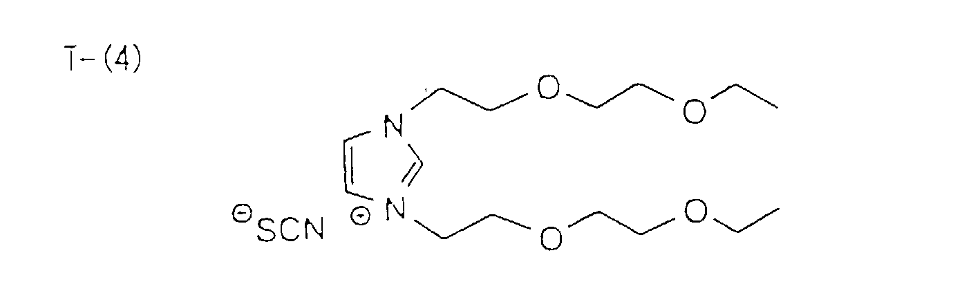
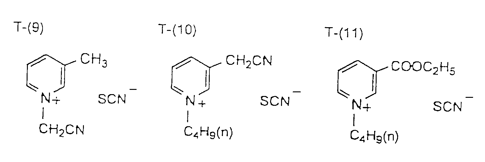
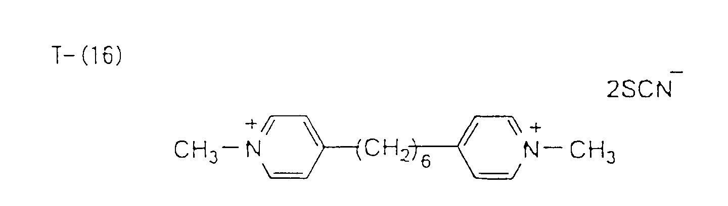
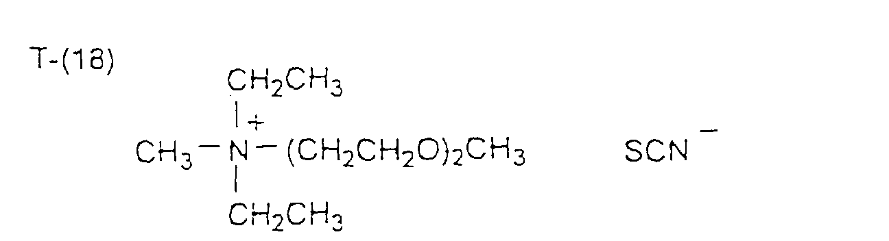
- Preferred examples of the thiocyanates used in the invention include alkali metal thiocyanates (for example, LiSCN, NaSCN, KSCN, RbSCN and CsSCN), substituted or unsubstituted ammonium thiocyanates, substituted or unsubstituted imidazolium thiocyanates, substituted or unsubstituted pyridinium thiocyanates, substituted or unsubstituted phosphonium thiocyanates, and thiocyanates having organic cations as counter ions.
- alkali metal thiocyanates for example, LiSCN, NaSCN, KSCN, RbSCN and CsSCN
- substituted or unsubstituted ammonium thiocyanates substituted or unsubstituted imidazolium thiocyanates
- substituted or unsubstituted imidazolium thiocyanates and substituted or unsubstituted pyridinium thiocyanates are particularly preferred, and the substituted or unsubstituted imidazolium thiocyanates are most preferred. Although they may be either solids or molten salts, the molten salts are preferred.
- substituent groups include an alkyl group (e.g., methyl, ethyl, isobutyl, n-dodecyl, cyclohexyl, vinyl, allyl or benzyl), an aryl group (e.g., phenyl or naphthyl), a heterocyclic residue (e.g., pyridyl, imidazolyl, furyl, thienyl, oxazolyl, benzimidazolyl or quinolyl), a halogen atom (e.g., fluorine, chlorine or bromine), an alkoxyl group (e.g., methoxy, ethoxy, benzyloxy or a group containing a plurality of ethyleneoxy groups), an aryloxy group (e.g., phenoxy), an alkylthio group (e.g., methylthio or ethylthio), an arylthio group (e.g.,
- thiocyanates may be used either alone or as a mixture of two or more of them.
- the total amount of the thiocyanate used is preferably from 0.2 mol% to less than 20 mol%, and more preferably from 0.5 mol% to less than 5 mol%, based on the p-type inorganic compound semiconductor.
- the charge transfer layer of the invention contains molten salts, in addition to the above-mentioned p-type inorganic compound semiconductor and thiocyanate, for further improving their durability.
- molten salts means ionic pure substances (salts) showing fluidity in the neighborhood of ordinary temperature or mixtures of the salts.
- molten salt of the pure substance at least one of a cation and an anion is usually an organic ion.
- at least one of ions of constituents is usually an organic ion. It is important that the molten salts added to the charge transfer layers of the invention do not substantially dissolve the p-type inorganic compound semiconductors.
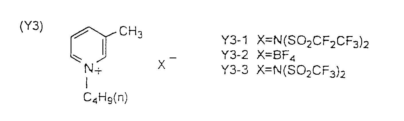
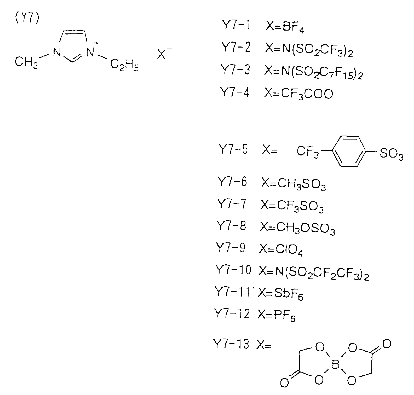
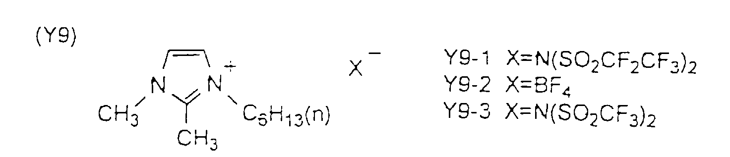
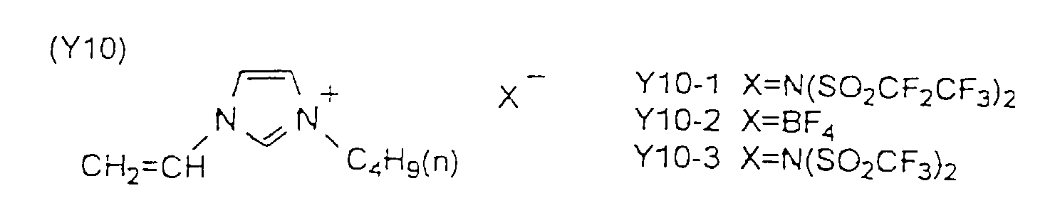
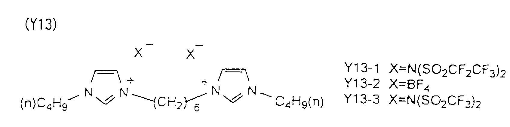
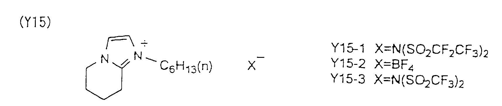
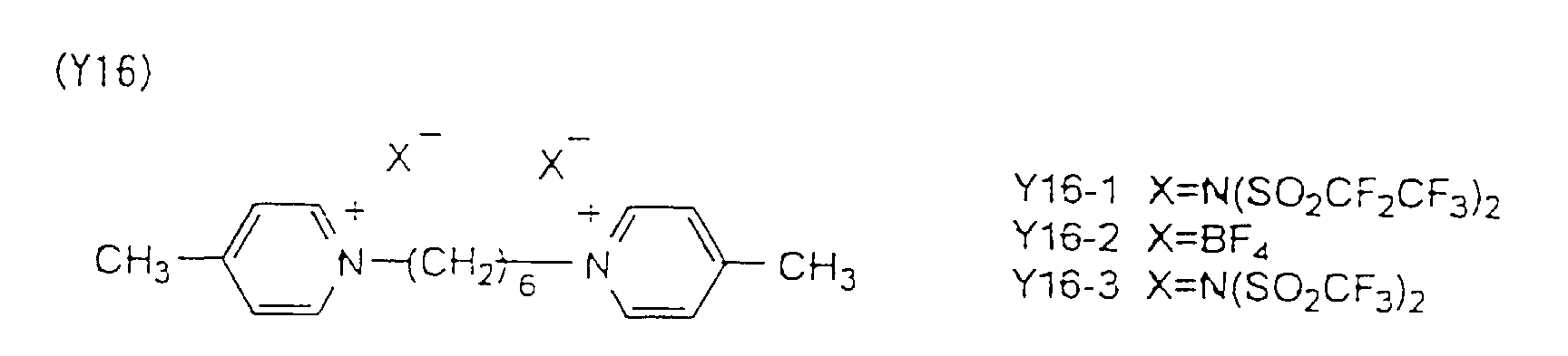
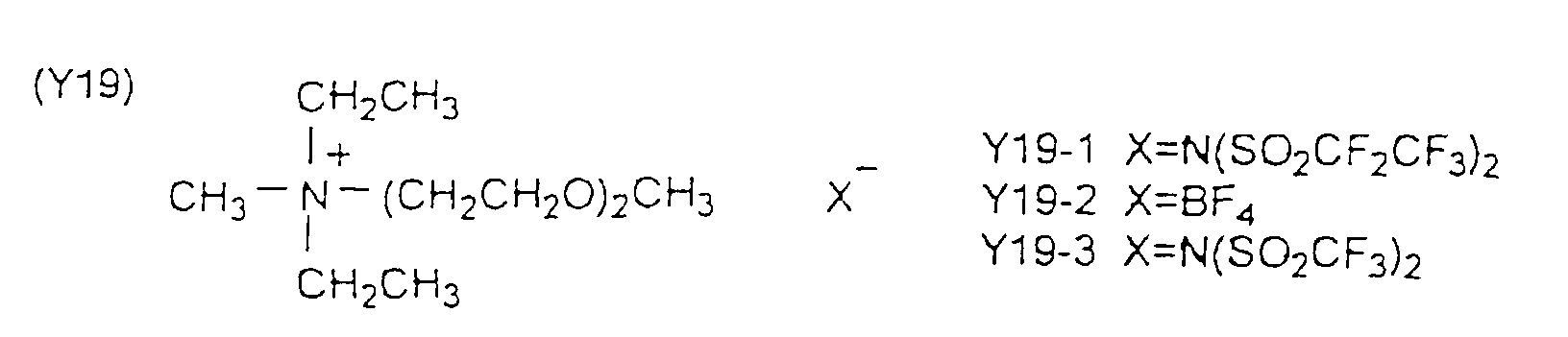
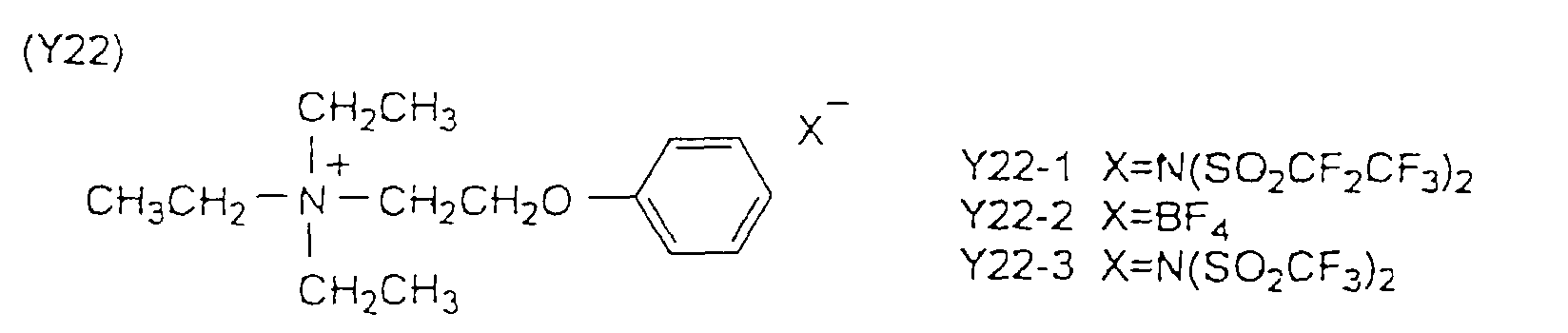
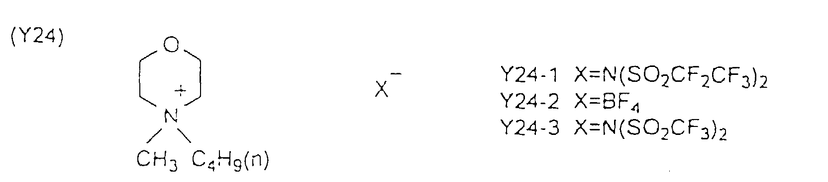
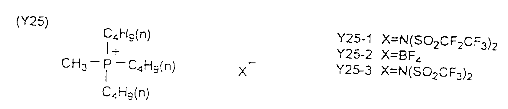
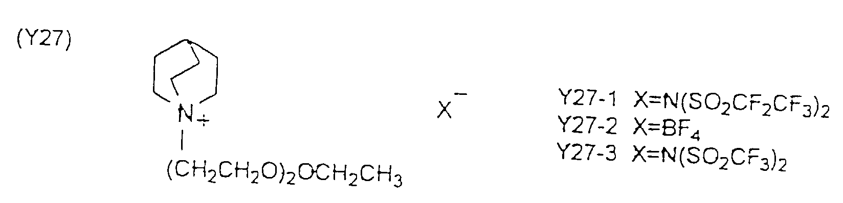
- the molten salts preferably used in the charge transfer layers include salts represented by any of the following general formulas (Y-a), (Y-b) and (Y-c):
- Q y1 represents an atomic group that can form a 5- or 6-membered aromatic cation together with a nitrogen atom.
- Q y1 is preferably composed of at least one atom selected from the group consisting of a carbon atom, a hydrogen atom, a nitrogen atom, an oxygen atom and a sulfur atom.
- the 5-membered ring formed by Q y1 is preferably an oxazole ring, a thiazole ring, an imidazole ring, a pyrazole ring, an isoxazole ring, a thiadiazole ring, an oxadiazole ring or a triazole ring, more preferably an oxazole ring, a thiazole ring, a triazole ring or an imidazole ring, and most preferably an imidazole ring.
- the 6-membered ring formed by Q y1 is preferably a pyridine ring, a pyrimidine ring, a pyridazine ring, a pyrazine ring or a triazine ring, and more preferably a pyridine ring.
- Q y1 may have a substituent group, and each of the substituent groups described above (for the thiocyanates) can be applied as the substituent group.
- the alkyl group, the alkoxyl group and the ethyleneoxy group-containing group are particularly preferred.
- R y1 represents a substituted or unsubstituted alkyl or alkenyl group having 1 to 24 carbon atoms.
- R y1 may be straight-chain, branched or cyclic.
- groups which can be preferably used include alkyl groups such as methyl, ethyl, propyl, isopropyl, pentyl, hexyl, octyl, 2-ethylhexyl, t-octyl, decyl, dodecyl, tetradecyl, 2-hexyldecyl, octadecyl, cyclohexyl and cyclopentyl, and alkenyl groups such as vinyl and allyl.
- R y1 has a substituent group, preferred examples thereof are the same as given for Q y1 .
- R y1 is preferably an alkyl group having from 2 to 18 carbon atoms or an alkenyl group having from 2 to 18 carbon atoms, and particularly preferably an alkyl group having from 2 to 6 carbon atoms.
- a y1 represents a nitrogen atom or a phosphorus atom.
- a y1 is preferably a nitrogen atom.
- R y1 to R y4 each represents a substituted or unsubstituted alkyl or alkenyl group having 1 to 24 carbon atoms as described for R y1 in general formula (Y-a). Two or more of R y2 to R y4 may be combined with each other to form a non-aromatic ring containing A y1 .
- R Y1 to R y4 have substituent groups, preferred examples thereof are the same as given for R y1 in general formula (Y-a).
- R y1 to R y4 are each preferably an, alkyl group having from 2 to 18 carbon atoms or an alkenyl group having from 2 to 18 carbon atoms, and particularly preferably an alkyl group having from 2 to 6 carbon atoms.
- Ryl to Ry6 in general formula (Y-c) have the same meaning as given for R y1 in general formula (Y-a). Two or more of R y1 to R y6 in general formula (Y-c) may be combined with each other to form a ring structure.
- R y1 to R y6 are each preferably an alkyl group having from 2 to 18 carbon atoms or an alkenyl group having from 2 to 18 carbon atoms, and particularly preferably an alkyl group having from 2 to 6 carbon atoms.
- X - represents a monovalent anion.
- the property of dissolving the p-type inorganic compound semiconductors, particularly compound semiconductors containing monovalent copper greatly depends on anion moieties. Anions strong in the property of dissolving the p-type inorganic compound semiconductors are unfavorable. Anions in which the pKa value of conjugate acids is 1 or less are preferred.
- X - preferably used in the invention is a perchlorate ion, a BF4 ion, a PF6 ion, an SbC16 ion, a CF3SO3 ion, a bis(perfluoroalkylsulfonylimide) ion or a tris(perfluoro-alkylsulfonylmethide) ion.
- the particularly preferred molten salts are bis(perfluoroalkylsulfonylimide) ions (for example, a bis(trifluoromethylsulfonyl)imide ion, a bis(pentafluoroethylsulfonyl)imide ion and a bis(heptadeca-fluorooctylsulfonyl)imide ion).
- the molten salts used in the invention are most preferably substituted or unsubstituted imidazolium bis(perfluoroalkylsulfonylimides).
- the compounds represented by general formula (Y-a), (Y-b) or (Y-c) may form polymers with the interposition of Q y1 or R y1 to R y6 .
- these molten salts when used in combination with the p-type inorganic compound semiconductors and the thiocyanates, the above-mentioned molten salts may be used either alone or as a mixture of two or more of them.
- the charge transfer layers of the invention can be improved in carrier concentration and conductivity by acceptor doping as needed.
- the doping may be either electrochemically conducted or chemically conducted using dopants.
- the dopants which are preferably used include but are not limited to iodine, tris(4-bromophenyl)aminium hexachloroantimonate, NOPF 6 , SbCl 5 , I 2 , Br 2 , HClO 4 , (n-C 4 H 9 ) 4 ClO 4 , trifluoroacetic acid, 4-dodecylbenzenesulfonic acid, 1-naphthalenesulfonic acid, FeCl 3 , AuCl 3 , NOSbF 6 , AsF 5 , NOBF 4 , LiBF 4 , H 3 [PMO 12 O 40 ], 7,7,8,8-tetracyanoquinodimethane (TCNQ) and Fullerene C60.
- the dopant is added, the
- a nitrile compound an organic compound having one or more cyano groups
- the nitrile compounds include cyanoalkylated product of saccharides such as sucrose, cellulose and amylose, and cyanoalkylated product of alcohols such as sorbitol and PVA.
- the thickness of the charge transfer layer of the invention is preferably from 0.005 ⁇ m to less than 100 ⁇ m, and more preferably from 0.01 ⁇ m to less than 50 ⁇ m, on the fine semiconductor particle-containing layer.
- the charge transfer layer of the invention is obtained by forming a layer containing the p-type inorganic compound semiconductor and the thiocyanate on the photosensitive layer (dye adsorbing semiconductor).
- the coating layer is formed by the coating.method
- additives such as binder resins difficult to trap holes and coating property improving agents such as leveling agents and surfactants can be added and dissolved to prepare a coating solution.
- the coating solution can be applied by spin coating, dip coating, air knife coating, curtain coating, roller coating, wire bar coating, gravure coating or extrusion coating using a hopper described in U.S. Patent 2,681,294 to form the charge transfer layers.
- solvents may be used.
- the solvent preferably used in coating includes nitriles (for example, acetonitrile, methoxyacetonitrile and methoxypropionitrile) and pyridine compounds (for example, pyridine and picoline). Of these, acetonitrile is particularly preferred.
- the solvent is removed under heating or reduced pressure during or after coating.
- the dye adsorption electrode is preferably heated upon coating.
- the substrate temperature upon coating is preferably from 30°C to less than 180°C, and more preferably from 40°C to less than 120°C.
- the molten salt may be added to the above-mentioned coating solution for the charge transfer layer.
- the molten salt may be added to the above-mentioned coating solution for the charge transfer layer.
- the impregnation of the molten salt can be carried out by overcoating the charge transfer layer containing the p-type inorganic compound semiconductor and the thiocyanate with the molten salt.
- Preferred examples of the overcoating method include a cast method, a spin coat method and an immersion method.
- deaeration is preferably conducted under reduced pressure. Then, excess molten salts are preferably soaked up with filter papers.
- the amount of the molten salt coated is from 0.1 g/m 2 to 10 g/m 2 , and more preferably from 0.5 g/m 2 to 5 g/m 2 .
- the counter electrode may have a single layer structure of a counter electrode conductive layer comprising a conductive material, or comprises a counter electrode conductive layer and a support substrate, similarly to the conductive support described above.
- the conductive material for use in the counter electrode conductive layer includes metals (for example, platinum, gold, silver, copper, aluminum, magnesium and indium), carbon and conductive metal oxides (indium-tin complex oxides and fluorine-doped tin oxide). Of these, platinum, gold, silver, copper, aluminum and magnesium can be preferably used as the counter electrode layer.
- the support substrate of the counter electrode is preferably made of glass or plastics, and used with the above-mentioned conductive material applied or vapor-deposited thereon.
- the thickness of the counter electrode conductive layer is preferably from 3 nm to 10 ⁇ m. It is preferred that the counter electrode layer is lower in surface resistance.
- the surface resistance is preferably 50 Q/square or less, and more preferably 20 ⁇ /square or less.
- Light may be irradiated from any one or both of the conductive support and the counter electrode, so that arrival of light at the photosensitive layer only requires that at least one of the conductive support and the counter electrode is substantially transparent.
- the conductive support is made transparent and light is irradiated from the conductive support side.
- the counter electrode has light-reflective properties.
- the counter electrode may be manufactured by directly coating, plating or vapor-depositing the charge transfer layer with the conductive material, or attaching the conductive layer-containing substrate to the charge transfer layer on its conductive layer side.
- a metal lead is preferably used for decreasing the resistance of the counter electrode, particularly when the counter electrode is transparent. Materials for the metal leads, methods for attaching them to the counter electrodes, and the reduction in the amount of incident light caused by the attachment of the metal leads are the same as with the conductive supports.
- a dense semiconductor film layer is previously provided as an undercoat layer between the conductive support and the photosensitive layer.
- the undercoat layer is preferably formed of TiO 2 , SnO 2 , Fe 2 O 3 , WO 3 , ZnO and Nb 2 O 5 , and more preferably TiO 2 .
- the undercoat layer can be provided by, for example, a sputtering method, as well as a spray pyrolysis method described in Electrochim. Acta, 40 , 643-652 (1995).
- the thickness of the undercoat layer is preferably from 5 nm to 1000 nm, and more preferably from 10 nm to 500 nm.
- a functional layer such as a protective layer or an anti-reflection layer may be provided on an outer surface or outer surfaces of one or both of the conductive support acting as an electrode and the counter electrode, between the conductive layer and the substrate, or in an intermediate portion of the substrate.
- coating methods, vapor deposition methods or attaching methods can be used depending on their materials.
- the internal structure of the photoelectric conversion device can take various forms depending on their purpose. Classifying them into two broad categories, a structure in which the incidence of light on both faces of the device is possible and a structure in which the incidence of light on only one face of the device is possible are available. Internal structures of the photoelectric conversion device, which can be preferably applied in the invention, are illustrated in Figs. 2 to 9.
- a photosensitive layer 20 and a charge transfer layer 30 are allowed to intervene between a transparent conductive layer 10a and a transparent counter electrode conductive layer 40a, resulting in a structure in which light is incident on both faces of the device.
- metal leads 11 are partly mounted on a transparent substrate 50a, a transparent conductive layer 10a is further provided thereon, a undercoat layer 60, a photosensitive layer 20, a charge transfer layer 30 and a counter electrode conductive layer 40 are formed in this order, and a support substrate 50 is further disposed, resulting in a structure in which light is incident on the conductive layer side of the device.
- a conductive layer 10 is further formed on a support substrate 50, a photosensitive layer 20 is provided with the interposition of an undercoat layer 60, a charge transfer layer 30 and a transparent counter electrode conductive layer 40a are further arranged thereon in this order, and a transparent substrate 50a partly provided with metal leads 11 is disposed thereon with the metal leads positioned inside, giving a structure in which light is incident on the counter electrode side of the device.
- metal leads 11 are partly mounted on a transparent substrate 50a, and a transparent conductive layer 10a (or 40a) is further provided thereon.
- an undercoat layer 60, a photosensitive layer 20 and a charge transfer layer 30 are allowed to intervene between the pair of sheets prepared above, giving a structure in which light is incident on both faces of the device.
- a transparent conductive layer 10a, a photosensitive layer 20, a charge transfer layer 30 and a counter electrode conductive layer 40 are provided on a transparent substrate 50a in this order, and a support substrate 50 is arranged thereon, giving a structure in which light is incident on the conductive layer side of the device.
- a conductive layer 10 is formed on a support substrate 50, a photosensitive layer 20 is provided with the interposition of an undercoat layer 60, a charge transfer layer 30 and a transparent counter electrode conductive layer 40a are further arranged thereon in this order, and a transparent substrate 50a is disposed thereon, giving a structure in which light is incident on the counter electrode side of the device.
- a transparent conductive layer 10a is formed on a transparent substrate 50a, a photosensitive layer 20 is provided with the interposition of an undercoat layer 60, a charge transfer layer 30 and a transparent counter electrode conductive layer 40a are further arranged thereon in this order, and a transparent substrate 50a is disposed thereon, resulting in a structure in which light is incident on both faces of the device.
- a conductive layer 10 is formed on a support substrate 50, a photosensitive layer 20 is provided with the interposition of an undercoat layer 60, a solid charge transfer layer 30 is further arranged thereon, and a partial counter electrode conductive layer 40 or metal leads 11 are provided thereon, resulting in a structure in which light is incident on the counter electrode side of the device.
- the photoelectric cell of the invention is a cell in which the above-mentioned photoelectric conversion device is allowed to do work by external loads.
- the photoelectric cells cells in which the charge transfer materials mainly comprise ion transfer materials are particularly called photoelectrochemical cells, and cells mainly aiming at electric power generation by solar light are called solar cells.
- the photoelectric cells are preferably sealed over their side faces with polymers or adhesives, for preventing deterioration of their constituents and evaporation of their contents.
- the external circuits themselves connected to the conductive supports and the counter electrodes through the leads may be known ones.
- the dye sensitization type solar cell of the invention can take a module structure basically similar to those of the conventional solar cells.
- the solar cell module generally has a structure in which the cell is constituted on a metal or ceramic support substrate, and covered with a filling resin or protective glass, thereby incorporating light from the side opposite to the support substrate.
- a transparent material such as tempered glass for the support substrate, and constituting the cell thereon, thereby incorporating light from the transparent support substrate side.
- module structures called the super straight type, the sub straight type and the potting type, and substrate-integral module structures used in amorphous silicon solar cells are known.
- the dye sensitization type solar cell of the invention can also be appropriately selected from these module structures, depending on the purpose for use, the place where they are used, and the circumstances. Specifically, structures and forms described in Japanese Patent Application No. 11-8457 are preferred. An example of the module structure is shown in Fig. 10.
- the adhesive tape was separated, followed by air drying at room temperature for 1 hour. Then, this glass was placed in an electric furnace (FP-32 type muffle furnace, manufactured by Yamato Scientific Co., Ltd.), and burned at 550°C for 30 minutes. Then, the glass was taken out, and cooled for 7 minutes, followed by immersion in a solution of Ru complex dye (R-1) in ethanol (3 X 10 -4 mol/liter) at room temperature for 12 hours. The dye-adsorbed glass was washed with acetonitrile, air-dried, and cut to 25 mm X 10 mm in width, thereby obtaining electrode A. The thickness of the photosensitive layer thus obtained (dye-adsorbed titanium oxide layer) was 4.0 ⁇ m, and the amount of the fine semiconductor particles coated was 6 g/m 2 .
- Charge transfer layer was formed by the following method.
- Thiocyanates shown in Table 1 were each added to and dissolved in a solution of CuI in acetonitrile (3.2 mass%) to prepare respective coating solutions.
- coating solutions were also prepared in the same manner as described above with the exception that no thiocyanates were contained.
- An exposed portion of the conductive face of electrode A prepared in (2) of Example and the periphery of a cell extending over 1 mm in width were protected with an adhesive tape, followed by standing on a hot plate heated at 100°C for 2 minutes. Then, 0.2 ml of each coating solution was slowly applied by use of an Eppendorf for about 10 minutes while evaporating acetonitrile, followed by standing on a hot plate for 2 hours to form a charge transfer layer.
- the thickness of the charge transfer layer formed at this time was from 15 ⁇ m to 30 ⁇ m.
- the electrode was coated with each molten salt shown in Table, and allowed to stand under a reduced pressure of 1000 Pa or less. Then, an excess molten salt was soaked up with a filter paper to remove it.
- the charge transfer layer formed as described above was overlaid with platinum-deposited glass (the thickness of a platinum layer: 1 ⁇ m, the thickness of glass: 1.1 mm, size: 1 cm X 2.5 cm), and pinched with a clip to prepare a photoelectric cell.
- platinum-deposited glass the thickness of a platinum layer: 1 ⁇ m, the thickness of glass: 1.1 mm, size: 1 cm X 2.5 cm
- photoelectric cells C-1 to C-12 and photoelectric cell RC-13 for comparison in each of which the glass 50a, the conductive layer 10a, the TiO2 undercoat layer 60, the dye adsorbed Tio2 electrode layer, the charge transfer layer 30 and the counter layer 40 were laminated in this order.
- a crocodile clip was connected to each of the conductive glass and the counter electrode of the above-mentioned photoelectric cell, the cell was irradiated with the simulated sunlight, and generated electricity was measured with a current-voltage measuring device (KEITHLEY, Type SMU 238) to determine the conversion efficiency. This measurement was conducted from 3 hours to 5 hours after preparation of the cell (measurement of initial performance). For examining the durability of the photoelectric cell, the photoelectric cell described above was stored under storage conditions of 40°C and 40% RH for 5 days, and then the photoelectric conversion performance was similarly measured again. The conversion efficiency in measurement of the initial performance and the conversion efficiency after storage are shown in Table 1. Cell No.
- a comparison between cells C-1 and C-2 of the invention and cells RC-14 and RC-15 containing no thiocyanates shows that the conversion efficiency and the durability are both significantly improved by the invention. Further, a comparison between cell C-13 and other cells of the invention shows that the use of the molten salt together with the thiocyanate is preferred in terms of the conversion efficiency and the durability.
- cells C-1 and C-2 are excellent in the conversion efficiency. It also indicates that the imidazolium salts are preferred as the thiocyanates. In a comparison of cells C-1 and C-7 to C-12, cells C-1, C-7, C-8, -11 and C-12 are excellent in the conversion efficiency and the durability. It also indicates that the bis(perfluoroalkylsulfonyl)imide salts are preferred as the molten salts.
- the photoelectric conversion devices of the invention using the p-type hole transfer materials are high in photoelectric conversion efficiency, and less in characteristic deterioration with time. Accordingly, the photoelectric cells comprising such photoelectric conversion devices are very effective as solar cells.
Landscapes
- Chemical & Material Sciences (AREA)
- Inorganic Chemistry (AREA)
- Physics & Mathematics (AREA)
- Electromagnetism (AREA)
- Photovoltaic Devices (AREA)
- Hybrid Cells (AREA)
- Electroluminescent Light Sources (AREA)
- Light Receiving Elements (AREA)
Abstract
Description
wherein said charge transfer layer comprises a p-type inorganic compound semiconductor and a thiocyanate.

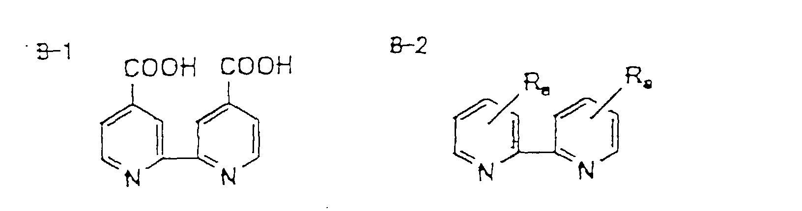
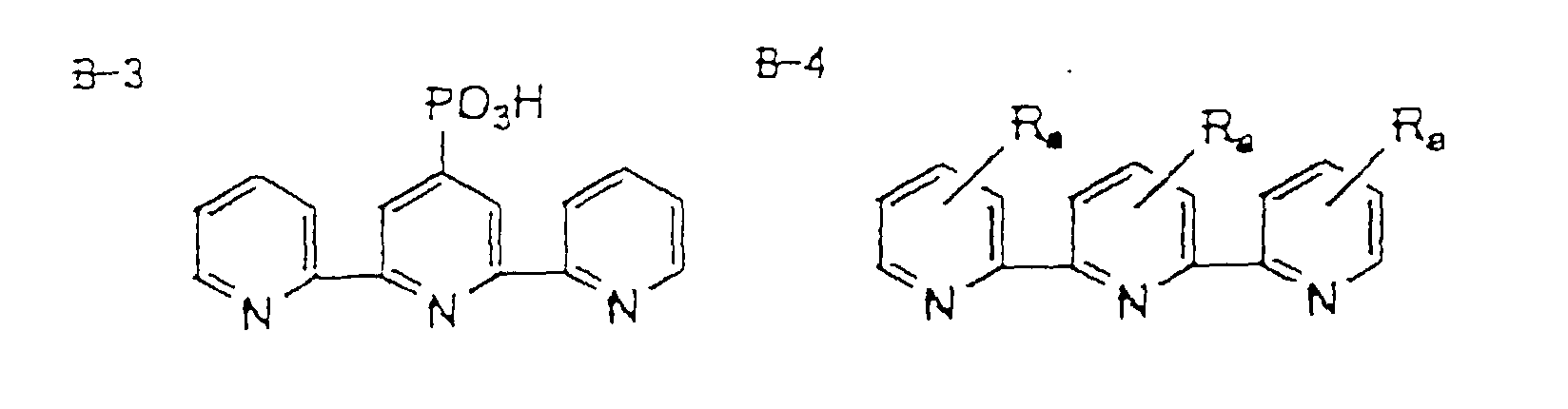


| No. | A, | p | B-a | B-b | B-c | Ra |
| R-1 | SCN | 2 | B-1 | B-1 | ― | ― |
| R-2 | CN | 2 | B-1 | B-1 | ― | ― |
| R-3 | Cl | 2 | B-1 | B-1 | ― | ― |
| R-4 | CN | 2 | B-7 | B-7 | ― | ― |
| R-5 | SCN | 2 | B-7 | B-7 | ― | ― |
| R-6 | SCN | 2 | B-1 | B-2 | ― | 4,4'-COO-N+(C4H9-n)4 |
| R-7 | SCN | 1 | B-1 | B-3 | ― | ― |
| R-8 | Cl | 1 | B-1 | B-4 | ― | H |
| R-9 | l | 2 | B-1 | B-5 | ― | H |
| R-10 | SCN | 3 | B-8 | ― | ― | ― |
| R-11 | CN | 3 | B-8 | ― | ― | ― |
| R-12 | SCN | 1 | B-8 | B-2 | ― | 4,4'-COO-N+(C4H9-n)4 |
| R-13 | ― | 0 | B-1 | B-1 | B-1 | ― |


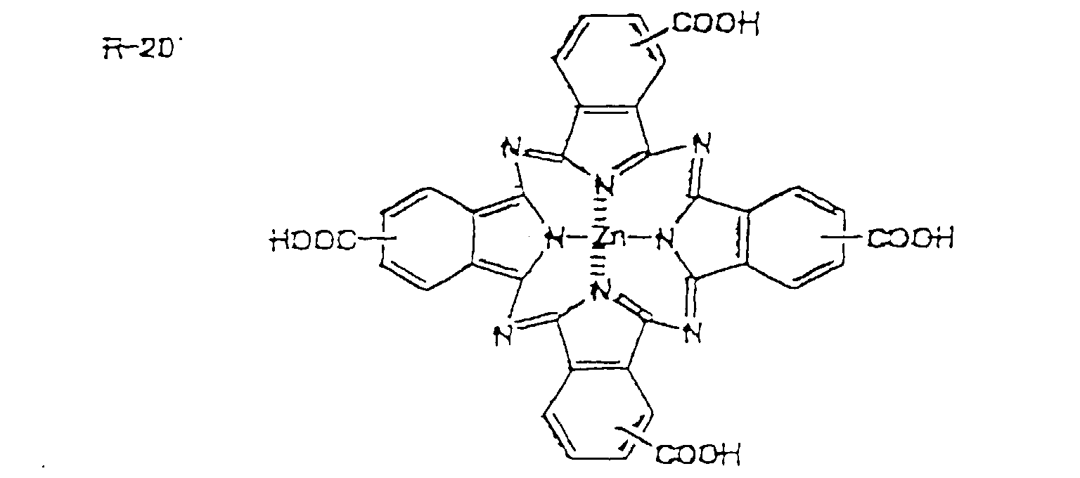


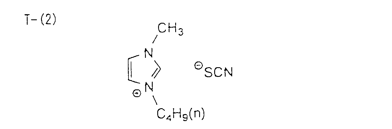








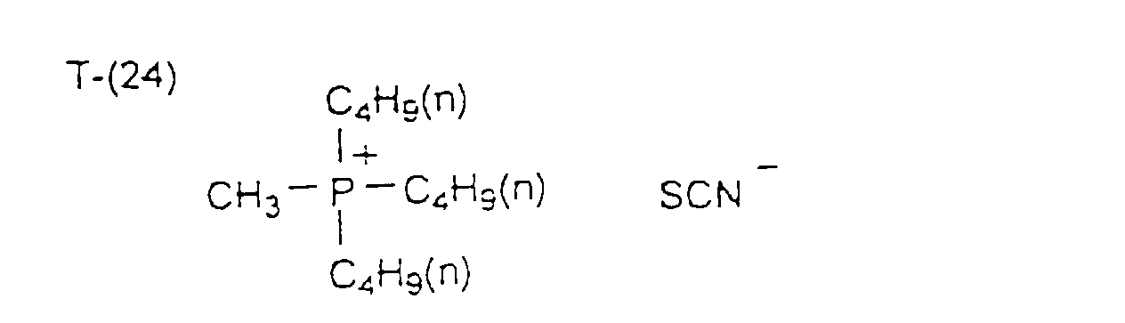
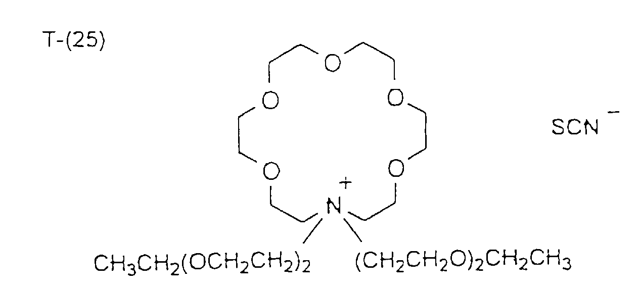

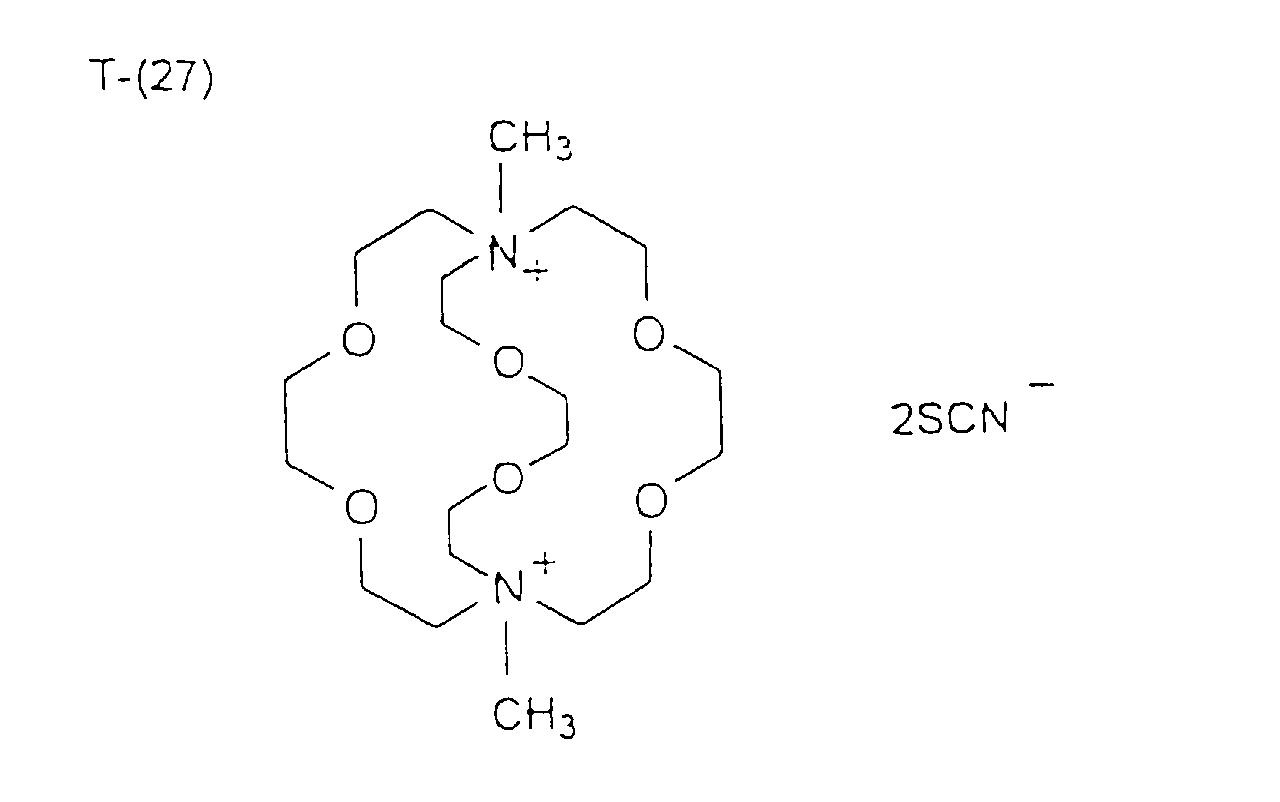


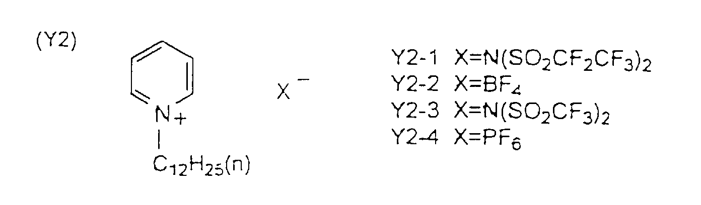












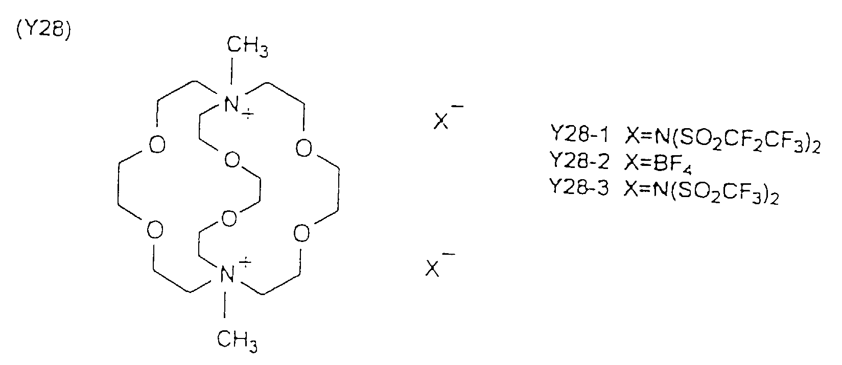


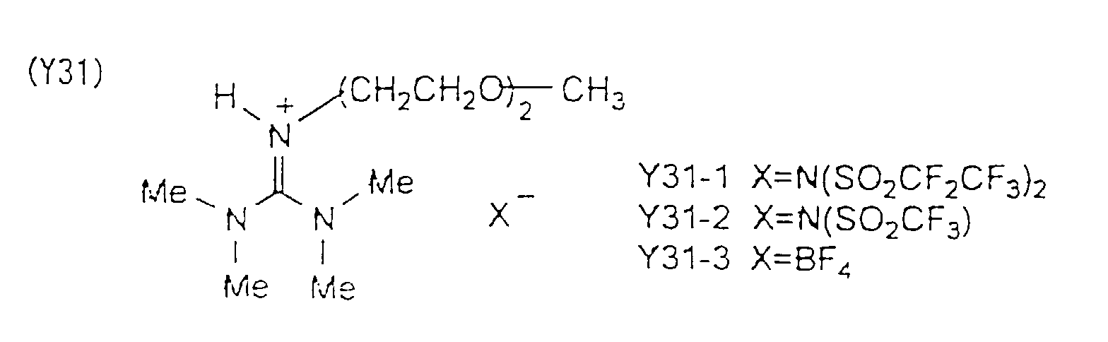
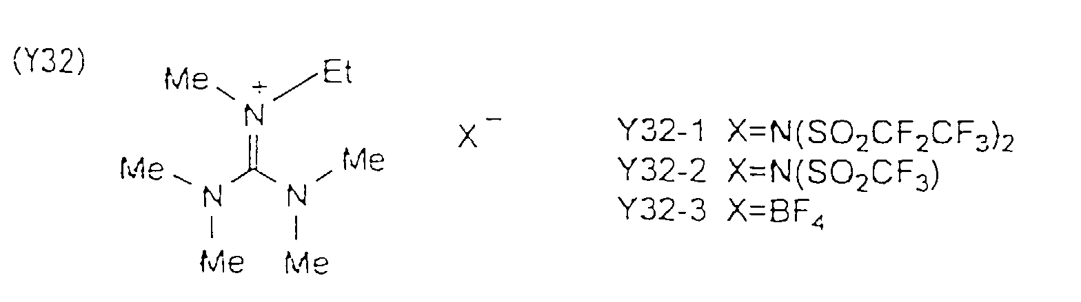
| Cell No. | Thiocyanate | Molten Salt | Initial Conversion Efficiency | Conversion Efficiency after Storage | |
| C-1 | Invention | T-(1) | Y7-2 | 3.5% | 3.4% |
| C-2 | Invention | T-(2) | Y7-2 | 3.4% | 3.3% |
| C-3 | Invention | T-(8) | Y7-2 | 2.9% | 2.7% |
| C-4 | Invention | T-(17) | Y7-2 | 2.9% | 2.7% |
| C-5 | Invention | NH4SCN | Y7-2 | 2.6% | 2.3% |
| C-6 | Invention | NaSCN | Y7-2 | 2.5% | 2.1% |
| C-7 | Invention | T-(1) | Y3-3 | 3.1% | 2.7% |
| C-8 | Invention | T-(1) | Y7-3 | 3.4% | 3.3% |
| C-9 | Invention | T-(1) | Y7-7 | 2.8% | 2.4% |
| C-10 | Invention | T-(1) | Y7-9 | 2.9% | 2.5% |
| C-11 | Invention | T-(1) | Y7-10 | 3.3% | 3.2% |
| C-12 | Invention | T-(1) | Y18-3 | 3.0% | 2.7% |
| C-13 | Invention | T-(1) | None | 2.2% | 1.5% |
| RC-14 | Comparison | None | Y7-2 | 1.2% | 0.8% |
| RC-15 | Comparison | None | None | 0.5% | 0.3% |
Claims (17)
- A photoelectric conversion device comprising a conductive layer, a photosensitive layer, a charge transfer layer and a counter electrode,
wherein said charge transfer layer comprises a p-type inorganic compound semiconductor and a thiocyanate. - The photoelectric conversion device according to claim 1, wherein said p-type inorganic compound semiconductor is a monovalent cupper-containing compound semiconductor.
- The photoelectric conversion device according to claim 2, wherein said monovalent cupper-containing compound semiconductor is CuI or CuSNC.
- The photoelectric conversion device according to any one of claims 1 to 3, wherein said thiocyanate is a molten salt.
- The photoelectric conversion device according to any one of claims 1 to 4, wherein said thiocyanate is a substituted or unsubstituted imidazolium thiocyanate or a substituted or unsubstituted pyridinium thiocyanate.
- The photoelectric conversion device according to any one of claims 1 to 5, wherein said thiocyanate is used in a molar amount of from not less than 0.2 mol% to less than 20 mol% based on the amount of the p-type inorganic compound semiconductor.
- The photoelectric conversion device according to any one of claims 1 to 6, wherein said charge transfer layer further contains a molten salt other than the thiocyanate.
- The photoelectric conversion device according to claim 7, wherein said molten salt other than the thiocyanate is represented by the following general formula (Y-a), (Y-b) or (Y-c):wherein Qy1 represents an atomic group which can form a 5-or 6-membered aromatic cation together with a nitrogen atom; Ry1, Ry2, Ry3, Ry4, Ry5 and Ry6 each independently represents a substituted or unsubstituted alkyl or alkenyl group having 1 to 24 carbon atoms; Ay1 represents a nitrogen atom or a phosphorus atom; and X- represents a monovalent anion.
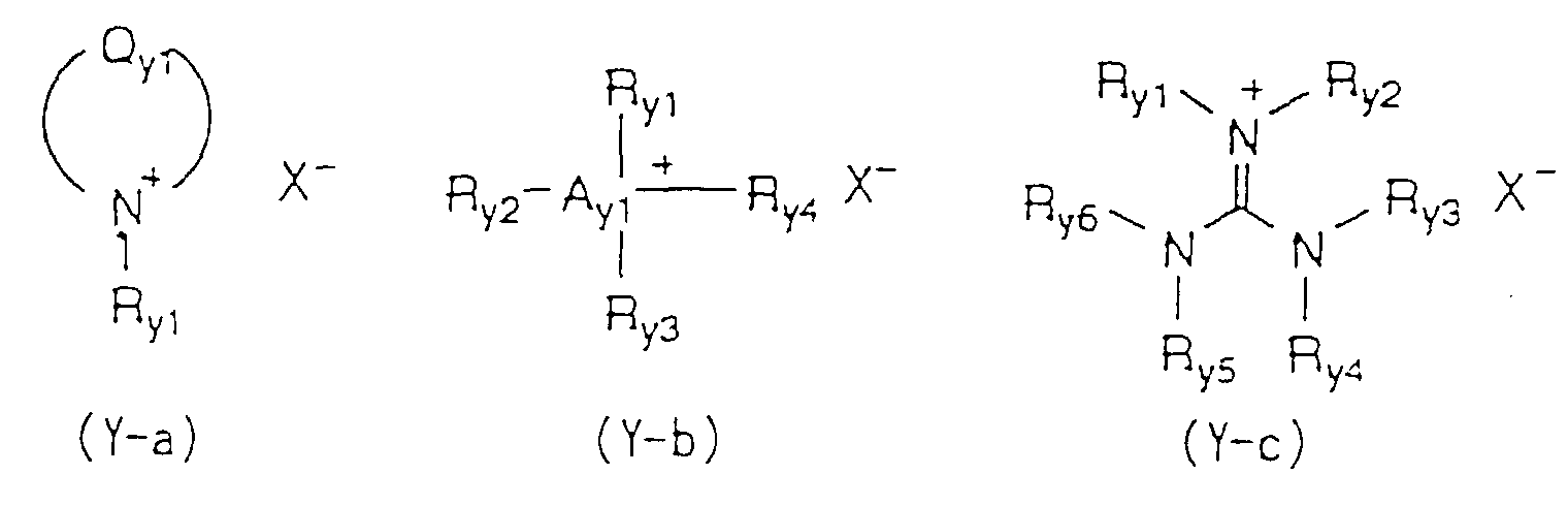
- The photoelectric conversion device according to claim 8, wherein Qyi in formula (Y-a) is an imidazole ring or a pyridine ring.
- The photoelectric conversion device according to claim 8, wherein X- of said molten salt is a bis (perfluoroalkylsulfonyl) imide anion.
- The photoelectric conversion device according to any one of claims 1 to 10, wherein said photosensitive layer contains fine semiconductor particles sensitized with a dye.
- The photoelectric conversion device according to claim 11, wherein said fine semiconductor particles are fine titanium dioxide particles.
- The photoelectric conversion device according to claim 11 or 12, wherein said dye is a ruthenium complex dye or a polymethine dye.
- The photoelectric conversion device according to any one of claims 1 to 13, wherein the photoelectric conversion device has an undercoat layer comprising an oxide semiconductor between said conductive layer and said photosensitive layer.
- A photoelectric cell using a photoelectric conversion device according to any one of claims 1 to 14.
- A solar cell module using a photoelectric conversion device according to any one of claims 1 to 14.
- A method for manufacturing a photoelectric conversion device comprising a conductive layer, a photosensitive layer, a charge transfer layer and a counter electrode, which comprises:forming, on the photosensitive layer, a first layer containing a p-type inorganic compound semiconductor and a thiocyanate; and thenovercoating said first layer with a molten salt to prepare said charge transfer layer.
Applications Claiming Priority (4)
| Application Number | Priority Date | Filing Date | Title |
|---|---|---|---|
| JP35183899 | 1999-12-10 | ||
| JP35183899 | 1999-12-10 | ||
| JP2000259216 | 2000-08-29 | ||
| JP2000259216A JP4307701B2 (en) | 1999-12-10 | 2000-08-29 | Photoelectric conversion element and photovoltaic cell |
Publications (3)
| Publication Number | Publication Date |
|---|---|
| EP1107333A2 true EP1107333A2 (en) | 2001-06-13 |
| EP1107333A3 EP1107333A3 (en) | 2005-01-05 |
| EP1107333B1 EP1107333B1 (en) | 2007-07-25 |
Family
ID=26579492
Family Applications (1)
| Application Number | Title | Priority Date | Filing Date |
|---|---|---|---|
| EP00126999A Expired - Lifetime EP1107333B1 (en) | 1999-12-10 | 2000-12-08 | Photoelectric conversion device and method of production |
Country Status (4)
| Country | Link |
|---|---|
| EP (1) | EP1107333B1 (en) |
| JP (1) | JP4307701B2 (en) |
| AT (1) | ATE368304T1 (en) |
| DE (1) | DE60035660T2 (en) |
Cited By (7)
| Publication number | Priority date | Publication date | Assignee | Title |
|---|---|---|---|---|
| EP1282189A4 (en) * | 2000-04-12 | 2003-07-30 | Hayashibara Biochem Lab | SEMICONDUCTOR LAYER, SOLAR CELL USING SAME, PRODUCTION METHODS AND APPLICATIONS THEREOF |
| NL1020701C2 (en) * | 2002-05-29 | 2003-12-02 | Stichting Energie | Method and device for applying a layer of a second material to a layer of a nanocrystalline first material. |
| US9183992B2 (en) | 2010-07-27 | 2015-11-10 | Shimane Prefectural Government | Dye-sensitized solar cell and method for preventing elution of catalyst from catalyst electrode |
| TWI669827B (en) * | 2014-03-14 | 2019-08-21 | 日商東京應化工業股份有限公司 | Crystal growth control agent, method for forming p-type semiconductor fine particles or p-type semiconductor fine particle film, composition for forming positive hole transport layer, and solar cell |
| EP2847807B1 (en) * | 2012-05-10 | 2019-11-27 | Merck Patent GmbH | Formulation comprising ionic organic compounds for use in electron transport layers |
| CN113972323A (en) * | 2021-10-11 | 2022-01-25 | 桂林理工大学 | Sodium thiocyanate-doped efficient and stable perovskite solar cell and preparation method thereof |
| CN116718643A (en) * | 2023-02-23 | 2023-09-08 | 艾感科技(广东)有限公司 | A semiconductor gas sensor based on a double-pass porous substrate |
Families Citing this family (8)
| Publication number | Priority date | Publication date | Assignee | Title |
|---|---|---|---|---|
| JP4643792B2 (en) * | 2000-03-31 | 2011-03-02 | 富士フイルム株式会社 | Photoelectric conversion element and photoelectrochemical cell |
| AU2003272969A1 (en) * | 2002-10-10 | 2004-05-04 | Kansai Paint Co., Ltd. | Method for forming semiconductor film and use of semiconductor film |
| JP5391981B2 (en) | 2009-02-02 | 2014-01-15 | 富士通株式会社 | Circuit board, manufacturing method thereof, and resistance element |
| JP5918236B2 (en) * | 2010-08-20 | 2016-05-18 | ロディア オペレーションズRhodia Operations | Polymer composition, polymer film, polymer gel, polymer foam, and electronic device containing the film, gel and foam |
| JP2012195280A (en) * | 2011-03-02 | 2012-10-11 | Sony Corp | Photoelectric conversion element, method for manufacturing photoelectric conversion element, electronic device, and building |
| JP5673344B2 (en) * | 2011-05-19 | 2015-02-18 | コニカミノルタ株式会社 | Dye-sensitized solar cell |
| CN105474338A (en) * | 2013-08-26 | 2016-04-06 | 日本瑞翁株式会社 | Light power generation device and method for manufacturing same |
| KR101985996B1 (en) * | 2016-03-10 | 2019-06-05 | 인하대학교 산학협력단 | Hole transporting material layer comprising copper thiocyanate(CuSCN) and preparation method thereof |
Family Cites Families (1)
| Publication number | Priority date | Publication date | Assignee | Title |
|---|---|---|---|---|
| JPH11144773A (en) * | 1997-09-05 | 1999-05-28 | Fuji Photo Film Co Ltd | Photoelectric conversion element and photoregeneration type photoelectrochemical cell |
-
2000
- 2000-08-29 JP JP2000259216A patent/JP4307701B2/en not_active Expired - Fee Related
- 2000-12-08 AT AT00126999T patent/ATE368304T1/en not_active IP Right Cessation
- 2000-12-08 EP EP00126999A patent/EP1107333B1/en not_active Expired - Lifetime
- 2000-12-08 DE DE60035660T patent/DE60035660T2/en not_active Expired - Lifetime
Cited By (10)
| Publication number | Priority date | Publication date | Assignee | Title |
|---|---|---|---|---|
| EP1282189A4 (en) * | 2000-04-12 | 2003-07-30 | Hayashibara Biochem Lab | SEMICONDUCTOR LAYER, SOLAR CELL USING SAME, PRODUCTION METHODS AND APPLICATIONS THEREOF |
| US6916981B2 (en) | 2000-04-12 | 2005-07-12 | Kabushiki Kaisha Hayashibara Seibutsu Kagaku Kenkyujo | Semiconductor layer, solar cell using it, and production methods and applications thereof |
| NL1020701C2 (en) * | 2002-05-29 | 2003-12-02 | Stichting Energie | Method and device for applying a layer of a second material to a layer of a nanocrystalline first material. |
| WO2003100801A1 (en) | 2002-05-29 | 2003-12-04 | Stichting Energieonderzoek Centrum Nederland | Method and apparatus for applying a layer of a second material to a layer of a nanocrystalline first material |
| US9183992B2 (en) | 2010-07-27 | 2015-11-10 | Shimane Prefectural Government | Dye-sensitized solar cell and method for preventing elution of catalyst from catalyst electrode |
| US9214287B2 (en) | 2010-07-27 | 2015-12-15 | Shimane Perfectual Government | Dye-sensitized solar cell and method for preventing elution of catalyst from catalyst electrode |
| EP2847807B1 (en) * | 2012-05-10 | 2019-11-27 | Merck Patent GmbH | Formulation comprising ionic organic compounds for use in electron transport layers |
| TWI669827B (en) * | 2014-03-14 | 2019-08-21 | 日商東京應化工業股份有限公司 | Crystal growth control agent, method for forming p-type semiconductor fine particles or p-type semiconductor fine particle film, composition for forming positive hole transport layer, and solar cell |
| CN113972323A (en) * | 2021-10-11 | 2022-01-25 | 桂林理工大学 | Sodium thiocyanate-doped efficient and stable perovskite solar cell and preparation method thereof |
| CN116718643A (en) * | 2023-02-23 | 2023-09-08 | 艾感科技(广东)有限公司 | A semiconductor gas sensor based on a double-pass porous substrate |
Also Published As
| Publication number | Publication date |
|---|---|
| JP4307701B2 (en) | 2009-08-05 |
| EP1107333B1 (en) | 2007-07-25 |
| DE60035660D1 (en) | 2007-09-06 |
| ATE368304T1 (en) | 2007-08-15 |
| JP2001230435A (en) | 2001-08-24 |
| DE60035660T2 (en) | 2007-12-27 |
| EP1107333A3 (en) | 2005-01-05 |
Similar Documents
| Publication | Publication Date | Title |
|---|---|---|
| JP4222466B2 (en) | Charge transport material, photoelectric conversion element and photovoltaic cell using the same, and pyridine compound | |
| JP5081345B2 (en) | Method for manufacturing photoelectric conversion element | |
| EP1089305B1 (en) | Electrolyte composition, photoelectric conversion device and photo-electrochemical cell | |
| EP1083582A2 (en) | Dye sensitized photoelectrochemical cell | |
| JP4617014B2 (en) | Method for manufacturing photoelectric conversion element | |
| EP1107333B1 (en) | Photoelectric conversion device and method of production | |
| JP2002008741A (en) | Photoelectric conversion element and photocell | |
| JP4453889B2 (en) | Electrolytic solution composition, photoelectric conversion element and photovoltaic cell | |
| JP2002105346A (en) | Metal complex dye, photoelectric conversion element and photocell | |
| JP2003187881A (en) | Photoelectric conversion element, method for manufacturing the same, and photoelectric cell | |
| JP4299960B2 (en) | Photoelectric conversion element and solar cell | |
| JP2002222968A (en) | Photoelectric conversion element and photoelectrochemical cell | |
| JP4970641B2 (en) | Photoelectric conversion element and photovoltaic cell using the same | |
| JP4278079B2 (en) | High sensitivity light receiving element and light sensor | |
| JP4217320B2 (en) | Photoelectric conversion element and photoelectrochemical cell | |
| JP4100491B2 (en) | Semiconductor fine particle layer, photoelectric conversion element and photovoltaic cell | |
| JP2004010403A (en) | Titanium oxide fine particle with multiple structure, method of producing the same, photoelectric conversion element and photoelectric cell comprising the same | |
| JP2001035253A (en) | Electrolyte composition, photoelectric transfer element and photo-electrochemical battery | |
| JP4958331B2 (en) | Method for producing photoelectric conversion element, photoelectric conversion element and photovoltaic cell | |
| JP4247810B2 (en) | Photoelectric conversion element and photovoltaic cell | |
| JP4578695B2 (en) | Method for creating photoelectric conversion element | |
| EP1174891A2 (en) | Dye sensitized photoelectrochemical cell | |
| JP5114536B2 (en) | Method for producing photoelectric conversion element, photoelectric conversion element and photoelectrochemical cell | |
| JP4072891B2 (en) | Method for manufacturing photoelectric conversion element and photovoltaic cell | |
| JP2001035552A (en) | Electrolyte composition, photoelectric converting element and photoelectric chemical battery |
Legal Events
| Date | Code | Title | Description |
|---|---|---|---|
| PUAI | Public reference made under article 153(3) epc to a published international application that has entered the european phase |
Free format text: ORIGINAL CODE: 0009012 |
|
| AK | Designated contracting states |
Kind code of ref document: A2 Designated state(s): AT BE CH CY DE DK ES FI FR GB GR IE IT LI LU MC NL PT SE TR |
|
| AX | Request for extension of the european patent |
Free format text: AL;LT;LV;MK;RO;SI |
|
| PUAL | Search report despatched |
Free format text: ORIGINAL CODE: 0009013 |
|
| AK | Designated contracting states |
Kind code of ref document: A3 Designated state(s): AT BE CH CY DE DK ES FI FR GB GR IE IT LI LU MC NL PT SE TR |
|
| AX | Request for extension of the european patent |
Extension state: AL LT LV MK RO SI |
|
| 17P | Request for examination filed |
Effective date: 20050225 |
|
| AKX | Designation fees paid |
Designated state(s): AT BE CH CY DE DK ES FI FR GB GR IE IT LI LU MC NL PT SE TR |
|
| 17Q | First examination report despatched |
Effective date: 20061122 |
|
| GRAP | Despatch of communication of intention to grant a patent |
Free format text: ORIGINAL CODE: EPIDOSNIGR1 |
|
| RAP1 | Party data changed (applicant data changed or rights of an application transferred) |
Owner name: FUJIFILM CORPORATION |
|
| RIC1 | Information provided on ipc code assigned before grant |
Ipc: H01L 51/42 20060101AFI20070207BHEP Ipc: H01G 9/20 20060101ALI20070207BHEP |
|
| RTI1 | Title (correction) |
Free format text: PHOTOELECTRIC CONVERSION DEVICE AND METHOD OF PRODUCTION |
|
| GRAS | Grant fee paid |
Free format text: ORIGINAL CODE: EPIDOSNIGR3 |
|
| GRAA | (expected) grant |
Free format text: ORIGINAL CODE: 0009210 |
|
| AK | Designated contracting states |
Kind code of ref document: B1 Designated state(s): AT BE CH CY DE DK ES FI FR GB GR IE IT LI LU MC NL PT SE TR |
|
| REG | Reference to a national code |
Ref country code: GB Ref legal event code: FG4D |
|
| REG | Reference to a national code |
Ref country code: CH Ref legal event code: EP |
|
| REG | Reference to a national code |
Ref country code: IE Ref legal event code: FG4D |
|
| REF | Corresponds to: |
Ref document number: 60035660 Country of ref document: DE Date of ref document: 20070906 Kind code of ref document: P |
|
| PG25 | Lapsed in a contracting state [announced via postgrant information from national office to epo] |
Ref country code: ES Free format text: LAPSE BECAUSE OF FAILURE TO SUBMIT A TRANSLATION OF THE DESCRIPTION OR TO PAY THE FEE WITHIN THE PRESCRIBED TIME-LIMIT Effective date: 20071105 Ref country code: NL Free format text: LAPSE BECAUSE OF FAILURE TO SUBMIT A TRANSLATION OF THE DESCRIPTION OR TO PAY THE FEE WITHIN THE PRESCRIBED TIME-LIMIT Effective date: 20070725 Ref country code: FI Free format text: LAPSE BECAUSE OF FAILURE TO SUBMIT A TRANSLATION OF THE DESCRIPTION OR TO PAY THE FEE WITHIN THE PRESCRIBED TIME-LIMIT Effective date: 20070725 Ref country code: PT Free format text: LAPSE BECAUSE OF FAILURE TO SUBMIT A TRANSLATION OF THE DESCRIPTION OR TO PAY THE FEE WITHIN THE PRESCRIBED TIME-LIMIT Effective date: 20071226 |
|
| REG | Reference to a national code |
Ref country code: CH Ref legal event code: PL |
|
| NLV1 | Nl: lapsed or annulled due to failure to fulfill the requirements of art. 29p and 29m of the patents act | ||
| PG25 | Lapsed in a contracting state [announced via postgrant information from national office to epo] |
Ref country code: CH Free format text: LAPSE BECAUSE OF FAILURE TO SUBMIT A TRANSLATION OF THE DESCRIPTION OR TO PAY THE FEE WITHIN THE PRESCRIBED TIME-LIMIT Effective date: 20070725 Ref country code: LI Free format text: LAPSE BECAUSE OF FAILURE TO SUBMIT A TRANSLATION OF THE DESCRIPTION OR TO PAY THE FEE WITHIN THE PRESCRIBED TIME-LIMIT Effective date: 20070725 Ref country code: AT Free format text: LAPSE BECAUSE OF FAILURE TO SUBMIT A TRANSLATION OF THE DESCRIPTION OR TO PAY THE FEE WITHIN THE PRESCRIBED TIME-LIMIT Effective date: 20070725 |
|
| EN | Fr: translation not filed | ||
| PG25 | Lapsed in a contracting state [announced via postgrant information from national office to epo] |
Ref country code: BE Free format text: LAPSE BECAUSE OF FAILURE TO SUBMIT A TRANSLATION OF THE DESCRIPTION OR TO PAY THE FEE WITHIN THE PRESCRIBED TIME-LIMIT Effective date: 20070725 |
|
| PG25 | Lapsed in a contracting state [announced via postgrant information from national office to epo] |
Ref country code: DK Free format text: LAPSE BECAUSE OF FAILURE TO SUBMIT A TRANSLATION OF THE DESCRIPTION OR TO PAY THE FEE WITHIN THE PRESCRIBED TIME-LIMIT Effective date: 20070725 Ref country code: GR Free format text: LAPSE BECAUSE OF FAILURE TO SUBMIT A TRANSLATION OF THE DESCRIPTION OR TO PAY THE FEE WITHIN THE PRESCRIBED TIME-LIMIT Effective date: 20071026 |
|
| PLBE | No opposition filed within time limit |
Free format text: ORIGINAL CODE: 0009261 |
|
| STAA | Information on the status of an ep patent application or granted ep patent |
Free format text: STATUS: NO OPPOSITION FILED WITHIN TIME LIMIT |
|
| PG25 | Lapsed in a contracting state [announced via postgrant information from national office to epo] |
Ref country code: SE Free format text: LAPSE BECAUSE OF FAILURE TO SUBMIT A TRANSLATION OF THE DESCRIPTION OR TO PAY THE FEE WITHIN THE PRESCRIBED TIME-LIMIT Effective date: 20071025 |
|
| 26N | No opposition filed |
Effective date: 20080428 |
|
| PG25 | Lapsed in a contracting state [announced via postgrant information from national office to epo] |
Ref country code: MC Free format text: LAPSE BECAUSE OF NON-PAYMENT OF DUE FEES Effective date: 20071231 Ref country code: FR Free format text: LAPSE BECAUSE OF FAILURE TO SUBMIT A TRANSLATION OF THE DESCRIPTION OR TO PAY THE FEE WITHIN THE PRESCRIBED TIME-LIMIT Effective date: 20080321 |
|
| GBPC | Gb: european patent ceased through non-payment of renewal fee |
Effective date: 20071208 |
|
| PG25 | Lapsed in a contracting state [announced via postgrant information from national office to epo] |
Ref country code: IE Free format text: LAPSE BECAUSE OF NON-PAYMENT OF DUE FEES Effective date: 20071210 |
|
| PG25 | Lapsed in a contracting state [announced via postgrant information from national office to epo] |
Ref country code: GB Free format text: LAPSE BECAUSE OF NON-PAYMENT OF DUE FEES Effective date: 20071208 |
|
| PG25 | Lapsed in a contracting state [announced via postgrant information from national office to epo] |
Ref country code: CY Free format text: LAPSE BECAUSE OF FAILURE TO SUBMIT A TRANSLATION OF THE DESCRIPTION OR TO PAY THE FEE WITHIN THE PRESCRIBED TIME-LIMIT Effective date: 20070725 |
|
| PG25 | Lapsed in a contracting state [announced via postgrant information from national office to epo] |
Ref country code: LU Free format text: LAPSE BECAUSE OF NON-PAYMENT OF DUE FEES Effective date: 20071208 |
|
| PG25 | Lapsed in a contracting state [announced via postgrant information from national office to epo] |
Ref country code: TR Free format text: LAPSE BECAUSE OF FAILURE TO SUBMIT A TRANSLATION OF THE DESCRIPTION OR TO PAY THE FEE WITHIN THE PRESCRIBED TIME-LIMIT Effective date: 20070725 |
|
| PG25 | Lapsed in a contracting state [announced via postgrant information from national office to epo] |
Ref country code: IT Free format text: LAPSE BECAUSE OF NON-PAYMENT OF DUE FEES Effective date: 20071231 |
|
| PGFP | Annual fee paid to national office [announced via postgrant information from national office to epo] |
Ref country code: DE Payment date: 20151201 Year of fee payment: 16 |
|
| REG | Reference to a national code |
Ref country code: DE Ref legal event code: R119 Ref document number: 60035660 Country of ref document: DE |
|
| PG25 | Lapsed in a contracting state [announced via postgrant information from national office to epo] |
Ref country code: DE Free format text: LAPSE BECAUSE OF NON-PAYMENT OF DUE FEES Effective date: 20170701 |