EP1107305A2 - Method for mounting a semiconductor device - Google Patents
Method for mounting a semiconductor device Download PDFInfo
- Publication number
- EP1107305A2 EP1107305A2 EP00127089A EP00127089A EP1107305A2 EP 1107305 A2 EP1107305 A2 EP 1107305A2 EP 00127089 A EP00127089 A EP 00127089A EP 00127089 A EP00127089 A EP 00127089A EP 1107305 A2 EP1107305 A2 EP 1107305A2
- Authority
- EP
- European Patent Office
- Prior art keywords
- metallic
- semiconductor device
- ultra
- fine particle
- fine particles
- Prior art date
- Legal status (The legal status is an assumption and is not a legal conclusion. Google has not performed a legal analysis and makes no representation as to the accuracy of the status listed.)
- Withdrawn
Links
Images



Classifications
-
- H—ELECTRICITY
- H05—ELECTRIC TECHNIQUES NOT OTHERWISE PROVIDED FOR
- H05K—PRINTED CIRCUITS; CASINGS OR CONSTRUCTIONAL DETAILS OF ELECTRIC APPARATUS; MANUFACTURE OF ASSEMBLAGES OF ELECTRICAL COMPONENTS
- H05K3/00—Apparatus or processes for manufacturing printed circuits
- H05K3/30—Assembling printed circuits with electric components, e.g. with resistors
- H05K3/32—Assembling printed circuits with electric components, e.g. with resistors electrically connecting electric components or wires to printed circuits
- H05K3/34—Assembling printed circuits with electric components, e.g. with resistors electrically connecting electric components or wires to printed circuits by soldering
- H05K3/341—Surface mounted components
- H05K3/3431—Leadless components
- H05K3/3436—Leadless components having an array of bottom contacts, e.g. pad grid array or ball grid array components
-
- H—ELECTRICITY
- H10—SEMICONDUCTOR DEVICES; ELECTRIC SOLID-STATE DEVICES NOT OTHERWISE PROVIDED FOR
- H10W—GENERIC PACKAGES, INTERCONNECTIONS, CONNECTORS OR OTHER CONSTRUCTIONAL DETAILS OF DEVICES COVERED BY CLASS H10
- H10W72/00—Interconnections or connectors in packages
-
- H—ELECTRICITY
- H10—SEMICONDUCTOR DEVICES; ELECTRIC SOLID-STATE DEVICES NOT OTHERWISE PROVIDED FOR
- H10W—GENERIC PACKAGES, INTERCONNECTIONS, CONNECTORS OR OTHER CONSTRUCTIONAL DETAILS OF DEVICES COVERED BY CLASS H10
- H10W72/00—Interconnections or connectors in packages
- H10W72/01—Manufacture or treatment
- H10W72/011—Apparatus therefor
- H10W72/0112—Apparatus for manufacturing bump connectors
-
- H—ELECTRICITY
- H10—SEMICONDUCTOR DEVICES; ELECTRIC SOLID-STATE DEVICES NOT OTHERWISE PROVIDED FOR
- H10W—GENERIC PACKAGES, INTERCONNECTIONS, CONNECTORS OR OTHER CONSTRUCTIONAL DETAILS OF DEVICES COVERED BY CLASS H10
- H10W72/00—Interconnections or connectors in packages
- H10W72/01—Manufacture or treatment
- H10W72/019—Manufacture or treatment of bond pads
-
- H—ELECTRICITY
- H10—SEMICONDUCTOR DEVICES; ELECTRIC SOLID-STATE DEVICES NOT OTHERWISE PROVIDED FOR
- H10W—GENERIC PACKAGES, INTERCONNECTIONS, CONNECTORS OR OTHER CONSTRUCTIONAL DETAILS OF DEVICES COVERED BY CLASS H10
- H10W72/00—Interconnections or connectors in packages
- H10W72/071—Connecting or disconnecting
- H10W72/0711—Apparatus therefor
-
- H—ELECTRICITY
- H05—ELECTRIC TECHNIQUES NOT OTHERWISE PROVIDED FOR
- H05K—PRINTED CIRCUITS; CASINGS OR CONSTRUCTIONAL DETAILS OF ELECTRIC APPARATUS; MANUFACTURE OF ASSEMBLAGES OF ELECTRICAL COMPONENTS
- H05K1/00—Printed circuits
- H05K1/02—Details
- H05K1/09—Use of materials for the conductive, e.g. metallic pattern
- H05K1/092—Dispersed materials, e.g. conductive pastes or inks
- H05K1/095—Dispersed materials, e.g. conductive pastes or inks for polymer thick films, i.e. having a permanent organic polymeric binder
-
- H—ELECTRICITY
- H05—ELECTRIC TECHNIQUES NOT OTHERWISE PROVIDED FOR
- H05K—PRINTED CIRCUITS; CASINGS OR CONSTRUCTIONAL DETAILS OF ELECTRIC APPARATUS; MANUFACTURE OF ASSEMBLAGES OF ELECTRICAL COMPONENTS
- H05K2201/00—Indexing scheme relating to printed circuits covered by H05K1/00
- H05K2201/02—Fillers; Particles; Fibers; Reinforcement materials
- H05K2201/0203—Fillers and particles
- H05K2201/0242—Shape of an individual particle
- H05K2201/0257—Nanoparticles
-
- H—ELECTRICITY
- H05—ELECTRIC TECHNIQUES NOT OTHERWISE PROVIDED FOR
- H05K—PRINTED CIRCUITS; CASINGS OR CONSTRUCTIONAL DETAILS OF ELECTRIC APPARATUS; MANUFACTURE OF ASSEMBLAGES OF ELECTRICAL COMPONENTS
- H05K2201/00—Indexing scheme relating to printed circuits covered by H05K1/00
- H05K2201/10—Details of components or other objects attached to or integrated in a printed circuit board
- H05K2201/10613—Details of electrical connections of non-printed components, e.g. special leads
- H05K2201/10621—Components characterised by their electrical contacts
- H05K2201/10674—Flip chip
-
- H—ELECTRICITY
- H10—SEMICONDUCTOR DEVICES; ELECTRIC SOLID-STATE DEVICES NOT OTHERWISE PROVIDED FOR
- H10W—GENERIC PACKAGES, INTERCONNECTIONS, CONNECTORS OR OTHER CONSTRUCTIONAL DETAILS OF DEVICES COVERED BY CLASS H10
- H10W72/00—Interconnections or connectors in packages
- H10W72/01—Manufacture or treatment
- H10W72/012—Manufacture or treatment of bump connectors, dummy bumps or thermal bumps
- H10W72/01215—Manufacture or treatment of bump connectors, dummy bumps or thermal bumps forming coatings
-
- H—ELECTRICITY
- H10—SEMICONDUCTOR DEVICES; ELECTRIC SOLID-STATE DEVICES NOT OTHERWISE PROVIDED FOR
- H10W—GENERIC PACKAGES, INTERCONNECTIONS, CONNECTORS OR OTHER CONSTRUCTIONAL DETAILS OF DEVICES COVERED BY CLASS H10
- H10W72/00—Interconnections or connectors in packages
- H10W72/01—Manufacture or treatment
- H10W72/012—Manufacture or treatment of bump connectors, dummy bumps or thermal bumps
- H10W72/01261—Chemical or physical modification, e.g. by sintering or anodisation
-
- H—ELECTRICITY
- H10—SEMICONDUCTOR DEVICES; ELECTRIC SOLID-STATE DEVICES NOT OTHERWISE PROVIDED FOR
- H10W—GENERIC PACKAGES, INTERCONNECTIONS, CONNECTORS OR OTHER CONSTRUCTIONAL DETAILS OF DEVICES COVERED BY CLASS H10
- H10W72/00—Interconnections or connectors in packages
- H10W72/071—Connecting or disconnecting
- H10W72/072—Connecting or disconnecting of bump connectors
-
- H—ELECTRICITY
- H10—SEMICONDUCTOR DEVICES; ELECTRIC SOLID-STATE DEVICES NOT OTHERWISE PROVIDED FOR
- H10W—GENERIC PACKAGES, INTERCONNECTIONS, CONNECTORS OR OTHER CONSTRUCTIONAL DETAILS OF DEVICES COVERED BY CLASS H10
- H10W72/00—Interconnections or connectors in packages
- H10W72/071—Connecting or disconnecting
- H10W72/073—Connecting or disconnecting of die-attach connectors
- H10W72/07331—Connecting techniques
- H10W72/07336—Soldering or alloying
-
- H—ELECTRICITY
- H10—SEMICONDUCTOR DEVICES; ELECTRIC SOLID-STATE DEVICES NOT OTHERWISE PROVIDED FOR
- H10W—GENERIC PACKAGES, INTERCONNECTIONS, CONNECTORS OR OTHER CONSTRUCTIONAL DETAILS OF DEVICES COVERED BY CLASS H10
- H10W72/00—Interconnections or connectors in packages
- H10W72/20—Bump connectors, e.g. solder bumps or copper pillars; Dummy bumps; Thermal bumps
- H10W72/241—Dispositions, e.g. layouts
-
- H—ELECTRICITY
- H10—SEMICONDUCTOR DEVICES; ELECTRIC SOLID-STATE DEVICES NOT OTHERWISE PROVIDED FOR
- H10W—GENERIC PACKAGES, INTERCONNECTIONS, CONNECTORS OR OTHER CONSTRUCTIONAL DETAILS OF DEVICES COVERED BY CLASS H10
- H10W72/00—Interconnections or connectors in packages
- H10W72/20—Bump connectors, e.g. solder bumps or copper pillars; Dummy bumps; Thermal bumps
- H10W72/251—Materials
-
- H—ELECTRICITY
- H10—SEMICONDUCTOR DEVICES; ELECTRIC SOLID-STATE DEVICES NOT OTHERWISE PROVIDED FOR
- H10W—GENERIC PACKAGES, INTERCONNECTIONS, CONNECTORS OR OTHER CONSTRUCTIONAL DETAILS OF DEVICES COVERED BY CLASS H10
- H10W72/00—Interconnections or connectors in packages
- H10W72/20—Bump connectors, e.g. solder bumps or copper pillars; Dummy bumps; Thermal bumps
- H10W72/251—Materials
- H10W72/252—Materials comprising solid metals or solid metalloids, e.g. PbSn, Ag or Cu
-
- H—ELECTRICITY
- H10—SEMICONDUCTOR DEVICES; ELECTRIC SOLID-STATE DEVICES NOT OTHERWISE PROVIDED FOR
- H10W—GENERIC PACKAGES, INTERCONNECTIONS, CONNECTORS OR OTHER CONSTRUCTIONAL DETAILS OF DEVICES COVERED BY CLASS H10
- H10W72/00—Interconnections or connectors in packages
- H10W72/30—Die-attach connectors
- H10W72/321—Structures or relative sizes of die-attach connectors
- H10W72/325—Die-attach connectors having a filler embedded in a matrix
-
- H—ELECTRICITY
- H10—SEMICONDUCTOR DEVICES; ELECTRIC SOLID-STATE DEVICES NOT OTHERWISE PROVIDED FOR
- H10W—GENERIC PACKAGES, INTERCONNECTIONS, CONNECTORS OR OTHER CONSTRUCTIONAL DETAILS OF DEVICES COVERED BY CLASS H10
- H10W72/00—Interconnections or connectors in packages
- H10W72/30—Die-attach connectors
- H10W72/351—Materials of die-attach connectors
- H10W72/352—Materials of die-attach connectors comprising metals or metalloids, e.g. solders
-
- H—ELECTRICITY
- H10—SEMICONDUCTOR DEVICES; ELECTRIC SOLID-STATE DEVICES NOT OTHERWISE PROVIDED FOR
- H10W—GENERIC PACKAGES, INTERCONNECTIONS, CONNECTORS OR OTHER CONSTRUCTIONAL DETAILS OF DEVICES COVERED BY CLASS H10
- H10W72/00—Interconnections or connectors in packages
- H10W72/90—Bond pads, in general
- H10W72/921—Structures or relative sizes of bond pads
- H10W72/923—Bond pads having multiple stacked layers
-
- H—ELECTRICITY
- H10—SEMICONDUCTOR DEVICES; ELECTRIC SOLID-STATE DEVICES NOT OTHERWISE PROVIDED FOR
- H10W—GENERIC PACKAGES, INTERCONNECTIONS, CONNECTORS OR OTHER CONSTRUCTIONAL DETAILS OF DEVICES COVERED BY CLASS H10
- H10W72/00—Interconnections or connectors in packages
- H10W72/90—Bond pads, in general
- H10W72/941—Dispositions of bond pads
- H10W72/9415—Dispositions of bond pads relative to the surface, e.g. recessed, protruding
-
- H—ELECTRICITY
- H10—SEMICONDUCTOR DEVICES; ELECTRIC SOLID-STATE DEVICES NOT OTHERWISE PROVIDED FOR
- H10W—GENERIC PACKAGES, INTERCONNECTIONS, CONNECTORS OR OTHER CONSTRUCTIONAL DETAILS OF DEVICES COVERED BY CLASS H10
- H10W90/00—Package configurations
- H10W90/701—Package configurations characterised by the relative positions of pads or connectors relative to package parts
- H10W90/721—Package configurations characterised by the relative positions of pads or connectors relative to package parts of bump connectors
- H10W90/724—Package configurations characterised by the relative positions of pads or connectors relative to package parts of bump connectors between a chip and a stacked insulating package substrate, interposer or RDL
-
- Y—GENERAL TAGGING OF NEW TECHNOLOGICAL DEVELOPMENTS; GENERAL TAGGING OF CROSS-SECTIONAL TECHNOLOGIES SPANNING OVER SEVERAL SECTIONS OF THE IPC; TECHNICAL SUBJECTS COVERED BY FORMER USPC CROSS-REFERENCE ART COLLECTIONS [XRACs] AND DIGESTS
- Y02—TECHNOLOGIES OR APPLICATIONS FOR MITIGATION OR ADAPTATION AGAINST CLIMATE CHANGE
- Y02P—CLIMATE CHANGE MITIGATION TECHNOLOGIES IN THE PRODUCTION OR PROCESSING OF GOODS
- Y02P70/00—Climate change mitigation technologies in the production process for final industrial or consumer products
- Y02P70/50—Manufacturing or production processes characterised by the final manufactured product
-
- Y—GENERAL TAGGING OF NEW TECHNOLOGICAL DEVELOPMENTS; GENERAL TAGGING OF CROSS-SECTIONAL TECHNOLOGIES SPANNING OVER SEVERAL SECTIONS OF THE IPC; TECHNICAL SUBJECTS COVERED BY FORMER USPC CROSS-REFERENCE ART COLLECTIONS [XRACs] AND DIGESTS
- Y10—TECHNICAL SUBJECTS COVERED BY FORMER USPC
- Y10T—TECHNICAL SUBJECTS COVERED BY FORMER US CLASSIFICATION
- Y10T29/00—Metal working
- Y10T29/49—Method of mechanical manufacture
- Y10T29/49002—Electrical device making
- Y10T29/49117—Conductor or circuit manufacturing
- Y10T29/49124—On flat or curved insulated base, e.g., printed circuit, etc.
- Y10T29/4913—Assembling to base an electrical component, e.g., capacitor, etc.
-
- Y—GENERAL TAGGING OF NEW TECHNOLOGICAL DEVELOPMENTS; GENERAL TAGGING OF CROSS-SECTIONAL TECHNOLOGIES SPANNING OVER SEVERAL SECTIONS OF THE IPC; TECHNICAL SUBJECTS COVERED BY FORMER USPC CROSS-REFERENCE ART COLLECTIONS [XRACs] AND DIGESTS
- Y10—TECHNICAL SUBJECTS COVERED BY FORMER USPC
- Y10T—TECHNICAL SUBJECTS COVERED BY FORMER US CLASSIFICATION
- Y10T29/00—Metal working
- Y10T29/49—Method of mechanical manufacture
- Y10T29/49002—Electrical device making
- Y10T29/49117—Conductor or circuit manufacturing
- Y10T29/49124—On flat or curved insulated base, e.g., printed circuit, etc.
- Y10T29/4913—Assembling to base an electrical component, e.g., capacitor, etc.
- Y10T29/49144—Assembling to base an electrical component, e.g., capacitor, etc. by metal fusion
-
- Y—GENERAL TAGGING OF NEW TECHNOLOGICAL DEVELOPMENTS; GENERAL TAGGING OF CROSS-SECTIONAL TECHNOLOGIES SPANNING OVER SEVERAL SECTIONS OF THE IPC; TECHNICAL SUBJECTS COVERED BY FORMER USPC CROSS-REFERENCE ART COLLECTIONS [XRACs] AND DIGESTS
- Y10—TECHNICAL SUBJECTS COVERED BY FORMER USPC
- Y10T—TECHNICAL SUBJECTS COVERED BY FORMER US CLASSIFICATION
- Y10T29/00—Metal working
- Y10T29/53—Means to assemble or disassemble
- Y10T29/5313—Means to assemble electrical device
- Y10T29/53174—Means to fasten electrical component to wiring board, base, or substrate
- Y10T29/53178—Chip component
Definitions
- This invention relates to a method for electrically connecting electrodes of a semiconductor device (chip, pellet or die) to terminal electrodes on a circuit board. More specifically, the invention relates to a method for mounting a semiconductor device by face down bonding using metallic paste for connection, or a method for mounting a semiconductor device which involves the use of solder bumps for electrical connection of electrodes; a mounted structure of a semiconductor device produced by any of these methods; and a mounting system for the methods and the mounted structure.
- Soldering has been generally used for electrical connection of connecting electrodes of an electronic device to circuit pattern terminals on a circuit board.
- a small package such as an IC flat package, has come into use, and the number of connecting terminals has increased.
- a so-called pitch between adjacent connecting terminals has gradually narrowed, and it has become gradually difficult for a conventional soldering technique to provide electrical connections stably in such a narrow pitch.
- the face down bonding method comprises forming solder bumps beforehand on electrode pads of the semiconductor device, placing the solder bumps so as to downwardly face terminal electrodes on the circuit board, and heating the solder bumps at a high temperature to fusion bond the electrode of semiconductor device to the terminal electrode of circuit board.
- the solder bumps are generally formed on three metallic thin films (under bump metals) comprising, for example, Cr (chromium), Cu (copper) and Au (gold), by soldering, plating or vapor deposition using a resist pattern.
- This mounting method imparts high mechanical strength after connection, and is capable of electrically connecting the plural electrodes of the semiconductor device to the terminal electrodes of the circuit board at a time. Thus, it has been considered an effective method for mounting a semiconductor device.
- the three metallic thin films comprising, for example, Cr (chromium), Cu (copper) and Au (gold) need to be formed prior to the formation of the solder bumps. Formation of these thin films has required not only considerably extensive equipment, but also mask management and vacuum management, thus leading to increase in the cost and working time. According to the conventional method of mounting a semiconductor device using solder bumps, moreover, the solder spreads during heat fusion, and the adjacent solder bumps (electrodes) may form short-circuit. Thus, this method may fail to be applied to micro-fabricated products.
- the metallic ultra-fine particles used in this method are considered to be ultra-fine particles of a metal alone which were prepared, for example, by the following method: A metal is evaporated in a vacuum in the presence of a small amount of gas to coagulate ultra-fine particles consisting only of metal from a vapor phase, thereby obtaining ultra-fine metallic particles.
- Such metallic ultra-fine particles may be problematical in stability, physical properties, and cost.
- An object of the present invention is to provide a method for mounting a semiconductor device, the method enabling the solder bump method to be conveniently performed, and being capable of realizing a highly stable, low-cost, high reliability electrical connection, and also provide a mounted structure by this method.
- Another object of the invention is to provide a method for mounting a semiconductor device, the method being capable of realizing a highly stable, low-cost, high reliability electrical connection, which has no risk of short-circuiting adjacent electrodes of even a narrow pitch; and a mounted structure of the semiconductor device produced by this method.
- the method, the structure and the system are characterized by using one of, or a combination of, the following two bump technologies:
- an aspect of the present invention is a method for mounting a semiconductor device, comprising: preparing a metallic ultra-fine particle paste by dispersing compound metallic ultra-fine particles in a solvent, the compound metallic ultra-fine particles each comprising a core portion consisting substantially of a metallic component and a coating layer chemically bound to the core portion and comprising an organic substance; forming ultra-fine particle electrodes by attaching the metallic fine particle paste onto electrodes of the semiconductor device, followed by low temperature heat process; forming solder bumps on the ultra-fine particle electrodes; and connecting the solder bumps to terminal electrodes of a circuit board by heat fusing thereof.
- the metallic fine particle paste is adhered onto the electrodes of the semiconductor device, and subjected to low temperature heat process.
- the ultra-fine particle electrodes which serve as under bump metals for solder bumps, can be formed easily and promptly without using extensive equipment.
- Another aspect of the present invention is a method for mounting a semiconductor device, comprising: preparing a metallic fine particle paste by dispersing compound metallic ultra-fine particles in a solvent, the compound metallic ultra-fine particles each comprising a core portion consisting substantially of a metallic component, and a coating layer chemically bound to the core portion and comprising an organic substance; forming metallic fine particle paste balls consisting mainly of the compound metallic ultra-fine particles by attaching the metallic fine particle paste onto terminal electrodes of a circuit board; connecting electrodes of the semiconductor device onto the metallic fine particle paste balls by the face down bonding method; and electrically connecting electrodes of the semiconductor device and the circuit board by low temperature heat process.
- the compound metallic ultra-fine particles can be prepared by a chemical process in a liquid phase. Thus, they can be mass produced in an ordinary atmospheric state, for a low cost, with the use of a simple apparatus without the need to use an extensive apparatus. Furthermore, the compound metallic ultra-fine particles have an organic substance as the coating layer. Thus, when in the solvent, these particles are minimally aggregatable, stable and easy to handle. Consequently, the metallic fine particle paste having the compound metallic ultra-fine particles uniformly dispersed therein can be prepared, and process control for the metallic fine particle paste is easy. Moreover, the particle diameters are uniform, so that all the compound metallic ultra-fine particles are fused and bound together at a constant temperature during low temperature heat treatment.
- the core portion is a positively charged, metallic ultra-fine particle of Ag, Au or Pb with an average particle diameter of 1 to 10 nm
- the coating layer is an organic anion having 5 or more carbon atoms.
- the low temperature heat process is performed in a temperature range of 200 to 300°C.
- the temperature is not lower than the temperature at which the coating layer is released from the core portion and core portions are fused and bound together.
- a compound metallic ultra-fine particle 14 comprising a core portion 10 and a coating layer 12 is prepared.
- the core portion 10 consists substantially of a metallic component, and the coating layer 12 comprises an organic substance.
- the compound metallic ultra-fine particle 14 has its core covered with the coating layer 12 comprising the organic substance.
- the compound metallic ultra-fine particle 14 is stable, and has a low tendency to aggregate in a solvent.
- the compound metallic ultra-fine particle 14 is composed of the organic substance and the metallic component, which is derived from a metal salt as a starting material, e.g., a carbonate, a formate or an acetate.
- the center portion of the compound metallic ultra-fine particle 14 comprises the metallic component, which is surrounded with an ionic organic substance.
- the organic substance and the metallic component are combined integrally, with part or all of them being chemically bonded together.
- the compound metallic ultra-fine particle 14 has high stability, and is also stable even at a higher metal concentration.
- the average particle diameter of the core portion 10 of the compound metallic ultra-fine particle 14 is 1 to 10 nm.
- the compound metallic ultra-fine particle 14 can be produced, for example, by heating a metal salt, such as a carbonate, formate or acetate, in a nonaqueous solvent and in the presence of an ionic organic substance, at a temperature not lower than the decomposition reduction temperature of the metal salt, but lower than the decomposition temperature of the ionic organic substance.
- a metal salt such as a carbonate, formate or acetate
- an ionic organic substance is suitably used.
- the ionic organic substance a fatty acid, an alkylbenzenesulfonic acid, or an alkylsulfonic acid, each having 5 or more carbon atoms, is used.
- the heating temperature is not lower than the decomposition reduction temperature of the metal salt such as a carbonate, formate or acetate, but lower than the decomposition temperature of the ionic organic substance.
- the temperature at which its decomposition begins is 200°C.
- silver acetate may be held at a temperature of higher than 200°C, and at a temperature at which the ionic organic substance is not decomposed.
- heating atmosphere is preferably inert gas atmosphere. By selecting a nonaqueous solvent, however, heating can be performed even in the air.
- various alcohols can be added, whereby the reaction can be promoted.
- the alcohols are not restricted, as long as the above effect is obtained.
- Their examples are lauryl alcohol, glycerin, and ethylene glycol.
- the amount of the alcohol added can be determined, as desired, depending on the type of the alcohol used. Normally, the alcohol may be added in an amount of about 5 to 20 parts by weight, preferably 5 to 10 parts by weight, with respect to 100 parts by weight of the metal salt.
- purification is performed by a publicly known purification method.
- the purification method may, for example, be centrifugation, membrane purification, or solvent extraction.
- oleic acid is used as an organic anionic substance
- silver acetate is used as a metal source.
- These materials are placed in a naphthenic high boiling solvent having a distillation point of 250°C.
- the mixture is heated for 3 hours at 240°C, and acetone is further added for precipitation and purification.
- compound metallic ultra-fine particles can be prepared.
- the compound metallic ultra-fine particles comprise clustered, positively charged Ag metallic ultra-fine particles (core metal) with an average particle diameter of about 10 nm, and organic anions (coating layer) coating the circumference of the metallic particles.
- the resulting compound metallic ultra-fine particles 14 are dispersed in a predetermined solvent such as toluene, and if desired, a resin or an additive is added to prepare a metallic paste.
- FIGS. 2A to FIG. 6 A first embodiment of the present invention will be described with reference to FIGS. 2A to FIG. 6.
- Such a metallic paste 44 is almost transparent and the physical properties of the metallic paste 24 such as surface tension and viscosity, can be adjusted by selecting the type of the solvent, the concentration of the compound metallic ultra-fine particles, and the temperature, as desired.
- the metallic paste 24 is subjected to low temperature heat process as shown in FIG. 2C(c), for example, at 200 to 300°C to form ultra-fine particle electrodes 26 comprising the core portions (metal) 10 of the compound metallic ultra-fine particles 14.
- the solvent, such as toluene, contained in the metallic paste 24 is evaporated.
- the compound metallic ultra-fine particles 24 as the main component of the metallic paste 24 are heated at a temperature not lower than the temperature at which the coating layer (organic substance) 12 (see FIGS. 1A and 1B) is released from the core portion 10 or the coating layer 12 itself is decomposed.
- the coating layer 12 is released from the core portion 10, or the coating layer 12 is decomposed to vanish.
- the core portions 10 are fused and bound together to form ultra-fine particle electrodes 26.
- the ultra-fine particle electrodes 26 serve as under bump metals for solder bumps 32.
- the ultra-fine particle electrode 26 can be formed easily and promptly without using extensive equipments such as expensive photolithography equipments or chemical vapor deposition equipments.
- the solder bumps 32 are formed on the ultra-fine particle electrodes 26, for example, by dipping the ultra-fine particle electrodes 26 in a molten solder bath 30 and lifting them, as shown by virtual lines in FIG. 4. The dipping is carried out by using solder bump forming device 27 including the molten solder bath 30.
- the solder bumps 32 may be formed on the ultra-fine particle electrodes 26 by printing a solder paste.
- the solder bumps 32 provided on the semiconductor device 20 are connected to predetermined positions on terminal electrodes 42 of a circuit board 40 by the flip chip bonding method in which the solder bumps 32 of the semiconductor device 20 and the terminal electrodes 42 of the circuit board 40 are aligned, with the semiconductor device 20 upside down in a face down manner.
- face down bonding is carried out by using bonding device 29.
- the resulting assembly is passed through, for example, a heat treatment furnace for reflow of the solder constituting the solder bumps 32 to perform heat fusing with the terminal electrodes 42 of the circuit board 40.
- a heat treatment furnace for reflow of the solder constituting the solder bumps 32 to perform heat fusing with the terminal electrodes 42 of the circuit board 40.
- the plurality of solder bumps 32 and the terminal electrodes 42 of the circuit board 40 can be electrically connected at a time.
- the solder bump method can be performed conveniently, and a highly stable, low-cost, high reliability electrical connection can be realized to mount a semiconductor device on a circuit board.
- mounting steps are preformed by a mounting system which uses printing device 23 for printing metallic paste as shown in FIG. 2C, lamp furnace 25 for forming under bump layer as shown in FIG. 2C, bonding device 29 for bonding semiconductor device 20 onto circuit board 40 as shown in FIG. 5, and furnace for heat treatment to form solder connections between solder bumps 32 and terminal electrodes 42 on the circuit board 40.
- the under metal layer 26 comprised by metallic ultra-fine particles fused and bound together is formed by printing device 23 and lamp furnace 25.
- the solder bump 32 is formed by solder bump forming device 27. Electrical connection between the bump and the terminal electrode is securely formed by the heat treatment furnace 31.
- the interposed devices 35 are utilities for stocking the products or cooling the products, etc.
- the mounting system is also equipped with load/unload device 37 and handling robot 39.
- Each device of the mounting system is controlled independently by a computer. However, informations of process steps are exchanged each other, and process informations are feed-back controlled. Thus optimum process control of the mounting system can be performed.
- FIGS. 7A, 7B, 7C, 7D and 7E Next, a second embodiment of the present invention will be described with reference to FIGS. 7A, 7B, 7C, 7D and 7E.
- the step of preparing a compound metallic ultra-fine particle 14 comprising a core portion 10 consisting substantially of a metallic component, and a coating layer 12 comprising an organic substance, as shown in FIGS. 1A and 1B, is the same as early described.
- the resulting compound metallic ultra-fine particles 14 are dispersed in a predetermined solvent such as toluene, and if desired, a metal having high electrical conductivity and measuring about 0.1 to 1 ⁇ m, such as Ag, Au, Pd or Al, and a resin or an additive is added to prepare a metallic paste.
- the metallic paste is dripped onto predetermined positions of terminal electrodes 42 of a circuit board 40 by using dripping device 54.
- the dripped paste forms about 2 ⁇ m high metallic paste balls 52 consisting mainly of the compound metallic ultra-fine particles 14 as shown in FIG. 7B.
- Such a metallic paste is almost transparent because when in a solvent in which the compound metallic ultra-fine particles 14 have been mixed and stirred, the compound metallic ultra-fine particles 14 are very fine.
- the physical properties of the metallic paste such as surface tension and viscosity, can be adjusted by selecting the type of the solvent, the concentration of the compound metallic ultra-fine particles, and the temperature, as desired.
- electrode pads provided on a semiconductor device 20 are connected onto the metallic paste balls 52, by the flip chip bonding device 56 in which the electrode pads of the semiconductor device 20 and the metallic paste balls 52 are aligned, with the semiconductor device 20 upside down in a face down manner. If desired, leveling is carried out with the use of the weight onto the semiconductor device 30. Then the semiconductor device 20 is bonded onto circuit board 40 via metallic paste balls 52 as shown in FIG. 7D.
- low temperature firing heat treatment
- a furnace 58 to form a conductor connector portion 53 which electrically connects the semiconductor device 20 and the circuit board 40.
- the solvent such as toluene
- the compound metallic ultra-fine particles 14 as the main component of the metallic paste balls 52 are heated at a temperature not lower than the temperature at which the coating layer (organic substance) 12 (see FIGS. 1A and 1B) is released from the core portion 10 or the coating layer 12 itself is decomposed.
- the coating layer 12 is released from the core portion 10, or the coating layer 12 is decomposed to vanish.
- the core portions 10 are fused and bound together to form metal conductor.
- low temperature heat process is performed, for example, in a temperature range of 200 to 250°C to connect the semiconductor device and the circuit board electrically.
- heat distortion minimally occurs.
- the absence of soldering can avoid a short circuit due to a flow of a solder, and connection with a finer pitch can be achieved.
- a metallic paste incorporating high conductivity metal particles as stated earlier, is used, high conductivity can be ensured via this metal conductor connection, and the reliability of mounting semiconductor device technology can be enhanced.
- the mounting system for mounting semiconductor devices comprises the dripping device 54 for forming the paste balls 52 as shown in FIG. 7A, the dryer for drying the dripped paste ball 52, the bonding device 56 for bonding semiconductor device 20 as shown in FIG. 7C, and the heat treatment furnace 58 for fusing ultra-fine metal particles to be bound together to form metal conductor as shown in FIG. 7E.
- These mounting devices are disposed integrally as shown in FIGS. 9 and 10, for example. Namely, dripping device 54, dryer 60 for paste balls, bonding device 56, heat treatment furnace 58 and load/unload device 62 are disposed integrally.
- Each device of the system is controlled independently by a computer. However, informations of every process step are exchanged each other, and process informations are feed-back controlled. Thus optimum process control of the system can be performed.
- the invention relates to a method for mounting a semiconductor device, comprising:
Landscapes
- Engineering & Computer Science (AREA)
- Manufacturing & Machinery (AREA)
- Microelectronics & Electronic Packaging (AREA)
- Wire Bonding (AREA)
- Electric Connection Of Electric Components To Printed Circuits (AREA)
Abstract
Description
- This invention relates to a method for electrically connecting electrodes of a semiconductor device (chip, pellet or die) to terminal electrodes on a circuit board. More specifically, the invention relates to a method for mounting a semiconductor device by face down bonding using metallic paste for connection, or a method for mounting a semiconductor device which involves the use of solder bumps for electrical connection of electrodes; a mounted structure of a semiconductor device produced by any of these methods; and a mounting system for the methods and the mounted structure.
- Soldering has been generally used for electrical connection of connecting electrodes of an electronic device to circuit pattern terminals on a circuit board. In recent years, a small package, such as an IC flat package, has come into use, and the number of connecting terminals has increased. Thus, a so-called pitch between adjacent connecting terminals has gradually narrowed, and it has become gradually difficult for a conventional soldering technique to provide electrical connections stably in such a narrow pitch.
- To mount a semiconductor device, such as a chip, pellet or die, which is an uncovered active or passive device, called a bare device, on a circuit board while establishing an electrical connection between them, face down bonding has recently been in wide use. The face down bonding method comprises forming solder bumps beforehand on electrode pads of the semiconductor device, placing the solder bumps so as to downwardly face terminal electrodes on the circuit board, and heating the solder bumps at a high temperature to fusion bond the electrode of semiconductor device to the terminal electrode of circuit board. The solder bumps are generally formed on three metallic thin films (under bump metals) comprising, for example, Cr (chromium), Cu (copper) and Au (gold), by soldering, plating or vapor deposition using a resist pattern.
- This mounting method imparts high mechanical strength after connection, and is capable of electrically connecting the plural electrodes of the semiconductor device to the terminal electrodes of the circuit board at a time. Thus, it has been considered an effective method for mounting a semiconductor device.
- In the conventional method of mounting a semiconductor device using solder bumps, however, the three metallic thin films (under bump metals) comprising, for example, Cr (chromium), Cu (copper) and Au (gold) need to be formed prior to the formation of the solder bumps. Formation of these thin films has required not only considerably extensive equipment, but also mask management and vacuum management, thus leading to increase in the cost and working time. According to the conventional method of mounting a semiconductor device using solder bumps, moreover, the solder spreads during heat fusion, and the adjacent solder bumps (electrodes) may form short-circuit. Thus, this method may fail to be applied to micro-fabricated products.
- It has been proposed to form balls from a metallic fine particle paste containing metallic ultra-fine particles, and use these balls instead of the above-mentioned solder bumps (see Japanese Laid-open Patent Publication No. 326416/1997). However, the metallic ultra-fine particles used in this method are considered to be ultra-fine particles of a metal alone which were prepared, for example, by the following method: A metal is evaporated in a vacuum in the presence of a small amount of gas to coagulate ultra-fine particles consisting only of metal from a vapor phase, thereby obtaining ultra-fine metallic particles. Such metallic ultra-fine particles may be problematical in stability, physical properties, and cost.
- The present invention has been accomplished in light of the foregoing circumstances. An object of the present invention is to provide a method for mounting a semiconductor device, the method enabling the solder bump method to be conveniently performed, and being capable of realizing a highly stable, low-cost, high reliability electrical connection, and also provide a mounted structure by this method. Another object of the invention is to provide a method for mounting a semiconductor device, the method being capable of realizing a highly stable, low-cost, high reliability electrical connection, which has no risk of short-circuiting adjacent electrodes of even a narrow pitch; and a mounted structure of the semiconductor device produced by this method.
- According to the present invention, there is provided a method, a structure and a system for mounting a semiconductor device by the bump technique using compound metallic ultra-fine particles each comprising a core portion consisting substantially of a metallic component, and a coating layer chemically bound to the core portion and comprising an organic substance. The method, the structure and the system are characterized by using one of, or a combination of, the following two bump technologies:
- 1) Forming under bump metals from the compound metallic ultra-fine particles, and forming ordinary solder balls on the under bump metals.
- 2) Using paste balls comprising the compound metallic ultra-fine particles, instead of ordinary solder balls.
-
- That is, an aspect of the present invention is a method for mounting a semiconductor device, comprising: preparing a metallic ultra-fine particle paste by dispersing compound metallic ultra-fine particles in a solvent, the compound metallic ultra-fine particles each comprising a core portion consisting substantially of a metallic component and a coating layer chemically bound to the core portion and comprising an organic substance; forming ultra-fine particle electrodes by attaching the metallic fine particle paste onto electrodes of the semiconductor device, followed by low temperature heat process; forming solder bumps on the ultra-fine particle electrodes; and connecting the solder bumps to terminal electrodes of a circuit board by heat fusing thereof.
- According to the above methods, the metallic fine particle paste is adhered onto the electrodes of the semiconductor device, and subjected to low temperature heat process. Thus, the ultra-fine particle electrodes, which serve as under bump metals for solder bumps, can be formed easily and promptly without using extensive equipment.
- Another aspect of the present invention is a method for mounting a semiconductor device, comprising: preparing a metallic fine particle paste by dispersing compound metallic ultra-fine particles in a solvent, the compound metallic ultra-fine particles each comprising a core portion consisting substantially of a metallic component, and a coating layer chemically bound to the core portion and comprising an organic substance; forming metallic fine particle paste balls consisting mainly of the compound metallic ultra-fine particles by attaching the metallic fine particle paste onto terminal electrodes of a circuit board; connecting electrodes of the semiconductor device onto the metallic fine particle paste balls by the face down bonding method; and electrically connecting electrodes of the semiconductor device and the circuit board by low temperature heat process.
- The compound metallic ultra-fine particles can be prepared by a chemical process in a liquid phase. Thus, they can be mass produced in an ordinary atmospheric state, for a low cost, with the use of a simple apparatus without the need to use an extensive apparatus. Furthermore, the compound metallic ultra-fine particles have an organic substance as the coating layer. Thus, when in the solvent, these particles are minimally aggregatable, stable and easy to handle. Consequently, the metallic fine particle paste having the compound metallic ultra-fine particles uniformly dispersed therein can be prepared, and process control for the metallic fine particle paste is easy. Moreover, the particle diameters are uniform, so that all the compound metallic ultra-fine particles are fused and bound together at a constant temperature during low temperature heat treatment.
- In the above methods for mounting a semiconductor device, the core portion is a positively charged, metallic ultra-fine particle of Ag, Au or Pb with an average particle diameter of 1 to 10 nm, and the coating layer is an organic anion having 5 or more carbon atoms.
- In the methods for mounting a semiconductor device, the low temperature heat process is performed in a temperature range of 200 to 300°C. The temperature is not lower than the temperature at which the coating layer is released from the core portion and core portions are fused and bound together.
- The above and other objects, features, and advantages of the present invention will be apparent from the following description when taken in conjunction with the accompanying drawings which illustrates preferred embodiments of the present invention by way of example.
-
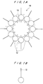
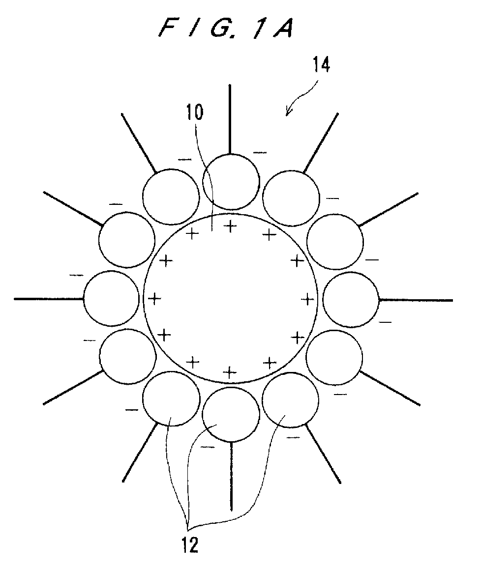
- FIGS. 1A and 1B are views schematically showing the structure of a compound metallic ultra-fine particle;
- FIGS. 2A to 6 are views showing a method for mounting a semiconductor device according to a first embodiment of the present invention in the order of steps;
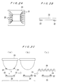
- FIGS. 2A and 2B are plan view and side view showing an example of the semiconductor device as an object to be mounted, and FIG. 2C shows steps (a)(b)(c) of forming under bump metal layer;
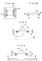
- FIGS. 3A and 3B are plan view and side view showing under bump layers adhered to electrodes of the semiconductor device illustrated in FIGS. 2A and 2B;
- FIG. 4 is a view in which virtual lines show the formation of solder bumps on the ultra-fine particle electrodes by solder bump forming device;
- FIG. 5 is a view showing a state immediately before bonding of the semiconductor device to a circuit board by bonding device;
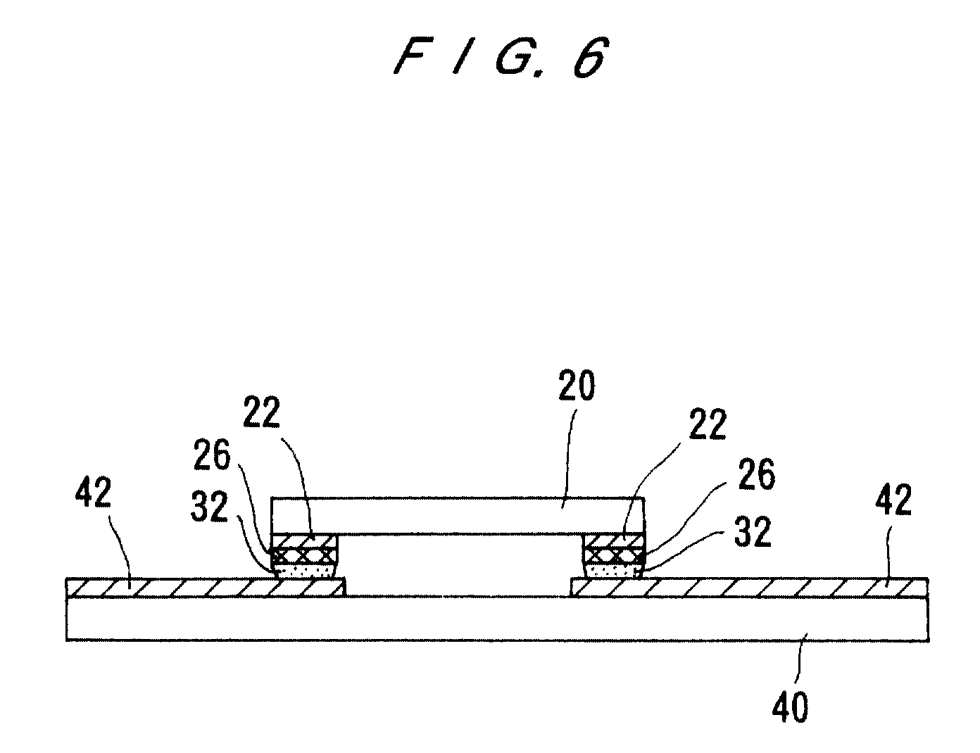
- FIG. 6 is a view showing a state immediately after bonding of the semiconductor device to the circuit board;
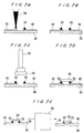
- FIG. 7A to 7E are views showing a method for mounting a semiconductor device according to a second embodiment of the present invention in the order of steps;
- FIG. 7A shows forming metallic paste balls onto terminal electrodes of the circuit board by dripping device;
- FIG. 7B shows that metallic paste balls are formed on the terminal electrodes of the circuit board;
- FIG. 7C shows face down bonding of the semiconductor device by bonding device;
- FIG. 7D shows that semiconductor device is bonded to the circuit board via metallic paste balls;
- FIG. 7E shows that electrical connections are formed between electrodes of semiconductor device and circuit board by passing through heat treatment furnace;
- FIG. 8 is a schematic view showing a mounting system configuration example according to the first embodiment;
- FIG. 9 is a plan view of a mounting system constituting an integral type according to the second embodiment; and
- FIG. 10 is an outside view of a mounting system of FIG. 9.
-
- Preferred embodiments of the present invention will now be described in detail with reference to the accompanying drawings.
- As shown in FIGS. 1A and 1B, a compound metallic
ultra-fine particle 14 comprising acore portion 10 and acoating layer 12 is prepared. Thecore portion 10 consists substantially of a metallic component, and thecoating layer 12 comprises an organic substance. The compound metallicultra-fine particle 14 has its core covered with thecoating layer 12 comprising the organic substance. Thus, the compound metallicultra-fine particle 14 is stable, and has a low tendency to aggregate in a solvent. - The compound metallic
ultra-fine particle 14 is composed of the organic substance and the metallic component, which is derived from a metal salt as a starting material, e.g., a carbonate, a formate or an acetate. The center portion of the compound metallicultra-fine particle 14 comprises the metallic component, which is surrounded with an ionic organic substance. The organic substance and the metallic component are combined integrally, with part or all of them being chemically bonded together. Unlike a conventional ultra-fine particle stabilized by coating with a surface active agent, the compound metallicultra-fine particle 14 has high stability, and is also stable even at a higher metal concentration. - The average particle diameter of the
core portion 10 of the compound metallicultra-fine particle 14 is 1 to 10 nm. By so constituting the compound metallicultra-fine particle 14, thecore portion 10 can be fused and bonded together at a considerably lower temperature than the melting point of the metal itself, whereby low temperature firing (formation of fused and bonded metal body) can be achieved. - The compound metallic
ultra-fine particle 14 can be produced, for example, by heating a metal salt, such as a carbonate, formate or acetate, in a nonaqueous solvent and in the presence of an ionic organic substance, at a temperature not lower than the decomposition reduction temperature of the metal salt, but lower than the decomposition temperature of the ionic organic substance. Regarding to the metallic component, Ag, Au or Pb is suitably used. As the ionic organic substance, a fatty acid, an alkylbenzenesulfonic acid, or an alkylsulfonic acid, each having 5 or more carbon atoms, is used. - The heating temperature is not lower than the decomposition reduction temperature of the metal salt such as a carbonate, formate or acetate, but lower than the decomposition temperature of the ionic organic substance. In the case of silver acetate, for example, the temperature at which its decomposition begins is 200°C. Thus, silver acetate may be held at a temperature of higher than 200°C, and at a temperature at which the ionic organic substance is not decomposed. In this case, in order to make the ionic organic substance difficult to decompose, heating atmosphere is preferably inert gas atmosphere. By selecting a nonaqueous solvent, however, heating can be performed even in the air.
- During heating, various alcohols can be added, whereby the reaction can be promoted. The alcohols are not restricted, as long as the above effect is obtained. Their examples are lauryl alcohol, glycerin, and ethylene glycol. The amount of the alcohol added can be determined, as desired, depending on the type of the alcohol used. Normally, the alcohol may be added in an amount of about 5 to 20 parts by weight, preferably 5 to 10 parts by weight, with respect to 100 parts by weight of the metal salt. After heating is completed, purification is performed by a publicly known purification method. The purification method may, for example, be centrifugation, membrane purification, or solvent extraction.
- As an example of production, oleic acid is used as an organic anionic substance, and silver acetate is used as a metal source. These materials are placed in a naphthenic high boiling solvent having a distillation point of 250°C. The mixture is heated for 3 hours at 240°C, and acetone is further added for precipitation and purification. In this manner, compound metallic ultra-fine particles can be prepared. The compound metallic ultra-fine particles comprise clustered, positively charged Ag metallic ultra-fine particles (core metal) with an average particle diameter of about 10 nm, and organic anions (coating layer) coating the circumference of the metallic particles. The resulting compound metallic
ultra-fine particles 14 are dispersed in a predetermined solvent such as toluene, and if desired, a resin or an additive is added to prepare a metallic paste. - A first embodiment of the present invention will be described with reference to FIGS. 2A to FIG. 6.
- A
semiconductor device 20 having a plurality ofaluminum electrodes 22 in a peripheral edge portion, as shown in FIGS. 2A and 2B, is prepared for use as a semiconductor device to be mounted. Ametallic paste 24, which has been prepared by dispersing the compound metallicultra-fine particles 14 in a predetermined solvent such as toluene, is applied onto each of theelectrodes 22, for example, by printingdevice 23, as shown in FIG. 2C(a)(b). Such a metallic paste 44 is almost transparent and the physical properties of themetallic paste 24 such as surface tension and viscosity, can be adjusted by selecting the type of the solvent, the concentration of the compound metallic ultra-fine particles, and the temperature, as desired. - Then, the
metallic paste 24 is subjected to low temperature heat process as shown in FIG. 2C(c), for example, at 200 to 300°C to formultra-fine particle electrodes 26 comprising the core portions (metal) 10 of the compound metallicultra-fine particles 14. In detail, during the low temperature heat process by thelamp furnace 25, the solvent, such as toluene, contained in themetallic paste 24 is evaporated. Furthermore, the compound metallicultra-fine particles 24 as the main component of themetallic paste 24 are heated at a temperature not lower than the temperature at which the coating layer (organic substance) 12 (see FIGS. 1A and 1B) is released from thecore portion 10 or thecoating layer 12 itself is decomposed. As a result, thecoating layer 12 is released from thecore portion 10, or thecoating layer 12 is decomposed to vanish. Simultaneously, thecore portions 10 are fused and bound together to formultra-fine particle electrodes 26. - As shown in FIGS. 3A and 3B, the
ultra-fine particle electrodes 26 serve as under bump metals for solder bumps 32. By so applying themetallic paste 24 onto theelectrodes 22, followed by low temperature heat process, theultra-fine particle electrode 26 can be formed easily and promptly without using extensive equipments such as expensive photolithography equipments or chemical vapor deposition equipments. - Then, the solder bumps 32 are formed on the
ultra-fine particle electrodes 26, for example, by dipping theultra-fine particle electrodes 26 in amolten solder bath 30 and lifting them, as shown by virtual lines in FIG. 4. The dipping is carried out by using solderbump forming device 27 including themolten solder bath 30. The solder bumps 32 may be formed on theultra-fine particle electrodes 26 by printing a solder paste. - Next, as shown in FIG. 5, the solder bumps 32 provided on the
semiconductor device 20 are connected to predetermined positions onterminal electrodes 42 of acircuit board 40 by the flip chip bonding method in which the solder bumps 32 of thesemiconductor device 20 and theterminal electrodes 42 of thecircuit board 40 are aligned, with thesemiconductor device 20 upside down in a face down manner. Such face down bonding is carried out by usingbonding device 29. - In this state, the resulting assembly is passed through, for example, a heat treatment furnace for reflow of the solder constituting the solder bumps 32 to perform heat fusing with the
terminal electrodes 42 of thecircuit board 40. In this manner, the plurality of solder bumps 32 and theterminal electrodes 42 of thecircuit board 40 can be electrically connected at a time. - According to this embodiment, as described above, the solder bump method can be performed conveniently, and a highly stable, low-cost, high reliability electrical connection can be realized to mount a semiconductor device on a circuit board.
- These mounting steps are preformed by a mounting system which uses
printing device 23 for printing metallic paste as shown in FIG. 2C,lamp furnace 25 for forming under bump layer as shown in FIG. 2C,bonding device 29 forbonding semiconductor device 20 ontocircuit board 40 as shown in FIG. 5, and furnace for heat treatment to form solder connections between solder bumps 32 andterminal electrodes 42 on thecircuit board 40. - These devices for constituting the mounting system are disposed as shown in FIG. 8, for example. The under
metal layer 26 comprised by metallic ultra-fine particles fused and bound together is formed by printingdevice 23 andlamp furnace 25. Thesolder bump 32 is formed by solderbump forming device 27. Electrical connection between the bump and the terminal electrode is securely formed by theheat treatment furnace 31. The interposeddevices 35 are utilities for stocking the products or cooling the products, etc. The mounting system is also equipped with load/unloaddevice 37 and handlingrobot 39. - Each device of the mounting system is controlled independently by a computer. However, informations of process steps are exchanged each other, and process informations are feed-back controlled. Thus optimum process control of the mounting system can be performed.
- Next, a second embodiment of the present invention will be described with reference to FIGS. 7A, 7B, 7C, 7D and 7E.
- The step of preparing a compound metallic
ultra-fine particle 14 comprising acore portion 10 consisting substantially of a metallic component, and acoating layer 12 comprising an organic substance, as shown in FIGS. 1A and 1B, is the same as early described. The resulting compound metallicultra-fine particles 14 are dispersed in a predetermined solvent such as toluene, and if desired, a metal having high electrical conductivity and measuring about 0.1 to 1 µ m, such as Ag, Au, Pd or Al, and a resin or an additive is added to prepare a metallic paste. - As shown in FIG. 7A, the metallic paste is dripped onto predetermined positions of
terminal electrodes 42 of acircuit board 40 by using drippingdevice 54. The dripped paste forms about 2 µ m highmetallic paste balls 52 consisting mainly of the compound metallicultra-fine particles 14 as shown in FIG. 7B. Such a metallic paste is almost transparent because when in a solvent in which the compound metallicultra-fine particles 14 have been mixed and stirred, the compound metallicultra-fine particles 14 are very fine. However, the physical properties of the metallic paste, such as surface tension and viscosity, can be adjusted by selecting the type of the solvent, the concentration of the compound metallic ultra-fine particles, and the temperature, as desired. - Then, as shown in FIG. 7C, electrode pads provided on a
semiconductor device 20 are connected onto themetallic paste balls 52, by the flipchip bonding device 56 in which the electrode pads of thesemiconductor device 20 and themetallic paste balls 52 are aligned, with thesemiconductor device 20 upside down in a face down manner. If desired, leveling is carried out with the use of the weight onto thesemiconductor device 30. Then thesemiconductor device 20 is bonded ontocircuit board 40 viametallic paste balls 52 as shown in FIG. 7D. - In this state, low temperature firing (heat treatment) is performed as shown in FIG. 7E, for example, for 30 minutes at 200 to 250°C by means of a
furnace 58 to form aconductor connector portion 53 which electrically connects thesemiconductor device 20 and thecircuit board 40. In detail, during the low temperature heat process, the solvent, such as toluene, contained in themetallic paste balls 52 is evaporated. Furthermore, the compound metallicultra-fine particles 14 as the main component of themetallic paste balls 52 are heated at a temperature not lower than the temperature at which the coating layer (organic substance) 12 (see FIGS. 1A and 1B) is released from thecore portion 10 or thecoating layer 12 itself is decomposed. As a result, thecoating layer 12 is released from thecore portion 10, or thecoating layer 12 is decomposed to vanish. Simultaneously, thecore portions 10 are fused and bound together to form metal conductor. - In this manner, low temperature heat process is performed, for example, in a temperature range of 200 to 250°C to connect the semiconductor device and the circuit board electrically. Thus, heat distortion minimally occurs. In addition, the absence of soldering can avoid a short circuit due to a flow of a solder, and connection with a finer pitch can be achieved. If a metallic paste incorporating high conductivity metal particles, as stated earlier, is used, high conductivity can be ensured via this metal conductor connection, and the reliability of mounting semiconductor device technology can be enhanced.
- As described above, a highly stable, low-cost, high reliability electrical connection with no risk of short-circuiting adjacent electrodes of even a narrow pitch can be realized to mount a semiconductor device on a circuit board.
- The mounting system for mounting semiconductor devices according to the embodiment comprises the dripping
device 54 for forming thepaste balls 52 as shown in FIG. 7A, the dryer for drying the drippedpaste ball 52, thebonding device 56 forbonding semiconductor device 20 as shown in FIG. 7C, and theheat treatment furnace 58 for fusing ultra-fine metal particles to be bound together to form metal conductor as shown in FIG. 7E. - These mounting devices are disposed integrally as shown in FIGS. 9 and 10, for example. Namely, dripping
device 54,dryer 60 for paste balls,bonding device 56,heat treatment furnace 58 and load/unloaddevice 62 are disposed integrally. - Each device of the system is controlled independently by a computer. However, informations of every process step are exchanged each other, and process informations are feed-back controlled. Thus optimum process control of the system can be performed.
- Although certain preferred embodiments of the present invention have been shown and described in detail, it should be understood that various changes and modifications may be made therein without departing from the scope of the appended claims.
- According to its broadest aspect the invention relates to a method for mounting a semiconductor device, comprising:
- preparing a metallic fine particle paste by dispersing
- compound metallic ultra-fine particles in a solvent, and
- forming ultra-fine particle electrodes by coating the metallic fine particle paste onto electrodes of the semiconductor device.
-
- It should be noted that the objects and advantages of the invention may be attained by means of any compatible combination(s) particularly pointed out in the items of the following summary of the invention.
-
- 1. A method for mounting a semiconductor device,
comprising:
- preparing a metallic fine particle paste by dispersing compound metallic ultra-fine particles in a solvent, the compound metallic ultra-fine particles each comprising a core portion consisting substantially of a metallic component, and a coating layer chemically bound to the core portion and comprising an organic substance;
- forming ultra-fine particle electrodes by coating the metallic fine particle paste onto electrodes of the semiconductor device, followed by low temperature heat process at a temperature not lower than the temperature at which the coating layer is released from the core portion and core portions are fused and bound together;
- forming solder bumps on the ultra-fine particle electrodes; and
- connecting the solder bumps to terminal electrodes of a circuit board by heat fusing of the solder.
- 2. The method for mounting a semiconductor device as claimed in item. 1, wherein the metallic fine particle paste has a metal and a resin added thereto, the metal having high conductivity and measuring about 0.1 to 1 µm.
- 3. The method for mounting a semiconductor device as
claimed in any one of item 1, wherein the core portion is
positively charged, and comprises metallic ultra-fine
particle of Ag, Au or Pb with an average particle diameter
of 1 to 10 nm, and
the coating layer is an organic anion having 5 or more carbon atoms. - 4. The method for mounting a semiconductor device as claimed in item 1, wherein the low temperature heat process is performed in a temperature range of 200 to 300°C.
- 5. A method for mounting a semiconductor device,
comprising:
- preparing a metallic fine particle paste by dispersing compound metallic ultra-fine particles in a solvent, the compound metallic ultra-fine particles each comprising a core portion consisting substantially of a metallic component, and a coating layer chemically bound to the core portion and comprising an organic substance;
- forming metallic fine particle paste balls consisting mainly of the compound metallic ultra-fine particles by attaching the metallic fine particle paste onto terminal electrodes of a circuit board;
- connecting electrodes of the semiconductor device onto the metallic fine particle paste balls by a face down bonding method; and
- forming ultra-fine particle electrodes from the paste balls by low temperature heat process at a temperature not lower than the temperature at which the coating layer is released from the core portion and core portions are fused and bound together, thereby electrically connecting the semiconductor device and the circuit board.
- 6. The method for mounting a semiconductor device as claimed in item 5, wherein the metallic fine particle paste has a metal and a resin added thereto, the metal having high conductivity and measuring about 0.1 to 1 µ m.
- 7. The method for mounting a semiconductor device as
claimed in any one of item 5, wherein the core portion is
positively charged, and comprises metallic ultra-fine
particle of Ag, Au or Pb with an average particle diameter
of 1 to 10 nm, and
the coating layer is an organic anion having 5 or more carbon atoms. - 8. The method for mounting a semiconductor device as claimed in item 5, wherein the low temperature heat process is performed in a temperature range of 200 to 300°C.
- 9. A mounted structure, comprising:
- a circuit board;
- a semiconductor device; and
- a connector portion for electrically connecting the semiconductor device and the circuit board, wherein the connector portion comprises a conductor portion that metallic ultra-fine particles are fused and bound together.
- 10. The mounted structure as claimed in item 9,
wherein the conductor portion has been formed by:
- dispersing compound metallic ultra-fine particles in a solvent to form a metallic fine particle paste, the compound metallic ultra-fine particles each comprising a core portion consisting substantially of a metallic component, and a coating layer chemically bound to the core portion and comprising an organic substance,
- attaching the metallic fine particle paste to a circuit board, or the semiconductor device; and
- performing low temperature heat process to the attached metallic fine particle paste so as to form the conductor portion.
- 11. The mounted structure as claimed in item 9, wherein the ultra-fine particles are metallic ultra-fine particles of Ag, Au or Pb having an average particle diameter of 1 to 10 nm.
- 12. The mounted structure as claimed in item 9, wherein the conductor portion comprises a bump portion on the circuit board, and connected to the semiconductor device.
- 13. The mounted structure as claimed in item 9, wherein the conductor portion is formed on the semiconductor device, and solder bump is formed on the conductor portion so as to connect to the electrode on the circuit board.
- 14. A semiconductor device mounting system comprising:
- a coating device for coating a metallic fine particle paste on an electrode of the semiconductor device or on an electrode on the circuit board, the paste having compound metallic ultra-fine particles each comprising a core portion consisting substantially of a metallic component, and a coating layer chemically bound to the core portion and comprising an organic substance; and
- a heat treatment furnace for forming a conductor portion from the paste by heat treatment at a temperature not lower than the temperature at which the coating layer is released from the core portion and core portions are fused and bound together.
- 15. The semiconductor device mounting system as claimed
in
item 14, wherein the coating device and the heat treatment furnace are integrally disposed in one unit. - 16. The semiconductor device mounting system as
claimed in
item 14, wherein the coating device and the heat treatment furnace are controlled independently, and are connected each other by a feedback mechanism. -
Claims (10)
- A method for mounting a semiconductor device, comprising:preparing a metallic fine particle paste by dispersing compound metallic ultra-fine particles in a solvent, the compound metallic ultra-fine particles each comprising a core portion consisting substantially of a metallic component, and a coating layer chemically bound to the core portion and comprising an organic substance;forming ultra-fine particle electrodes by coating the metallic fine particle paste onto electrodes of the semiconductor device, followed by low temperature heat process at a temperature not lower than the temperature at which the coating layer is released from the core portion and core portions are fused and bound together;forming solder bumps on the ultra-fine particle electrodes; andconnecting the solder bumps to terminal electrodes of a circuit board by heat fusing of the solder.
- The method for mounting a semiconductor device as claimed in claim 1, wherein the metallic fine particle paste has a metal and a resin added thereto, the metal having high conductivity and measuring about 0.1 to 1 µ m.
- The method for mounting a semiconductor device as claimed in any one of claim 1, wherein the core portion is positively charged, and comprises metallic ultra-fine particle of Ag, Au or Pb with an average particle diameter of 1 to 10 nm, and
the coating layer is an organic anion having 5 or more carbon atoms, and/ or wherein preferably the low temperature heat process is performed in a temperature range of 200 to 300°C. - A method for mounting a semiconductor device, comprising:preparing a metallic fine particle paste by dispersing compound metallic ultra-fine particles in a solvent, the compound metallic ultra-fine particles each comprising a core portion consisting substantially of a metallic component, and a coating layer chemically bound to the core portion and comprising an organic substance;forming metallic fine particle paste balls consisting mainly of the compound metallic ultra-fine particles by attaching the metallic fine particle paste onto terminal electrodes of a circuit board;connecting electrodes of the semiconductor device onto the metallic fine particle paste balls by a face down bonding method; andforming ultra-fine particle electrodes from the paste balls by low temperature heat process at a temperature not lower than the temperature at which the coating layer is released from the core portion and core portions are fused and bound together, thereby electrically connecting the semiconductor device and the circuit board.
- The method for mounting a semiconductor device as claimed in claim 4 , wherein the metallic fine particle paste has a metal and a resin added thereto, the metal having high conductivity and measuring about 0.1 to 1 µm.and/ or wherein preferably the core portion is positively charged, and comprises metallic ultra-fine particle of Ag, Au or Pb with an average particle diameter of 1 to 10 nm, and
the coating layer is an organic anion having 5 or more carbon atoms,and/ or wherein preferably the low temperature heat process is performed in a temperature range of 200 to 300°C. - A mounted structure, comprising:a circuit board;a semiconductor device; anda connector portion for electrically connecting the semiconductor device and the circuit board, wherein the connector portion comprises a conductor portion that metallic ultra-fine particles are fused and bound together.
- The mounted structure as claimed in claim 9, wherein the conductor portion has been formed by:dispersing compound metallic ultra-fine particles in a solvent to form a metallic fine particle paste, the compound metallic ultra-fine particles each comprising a core portion consisting substantially of a metallic component, and a coating layer chemically bound to the core portion and comprising an organic substance,attaching the metallic fine particle paste to a circuit board, or the semiconductor device; andperforming low temperature heat process to the attached metallic fine particle paste so as to form the conductor portion,and/ or wherein preferably the ultra-fine particles are metallic ultra-fine particles of Ag, Au or Pb having an average particle diameter of 1 to 10 nm,and/ or wherein preferably the conductor portion comprises a bump portion on the circuit board, and connected to the semiconductor device,and/ or wherein preferably the conductor portion is formed on the semiconductor device, and solder bump is formed on the conductor portion so as to connect to the electrode on the circuit board.
- A semiconductor device mounting system comprising:a coating device for coating a metallic fine particle paste on an electrode of the semiconductor device or on an electrode on the circuit board, the paste having compound metallic ultra-fine particles each comprising a core portion consisting substantially of a metallic component, and a coating layer chemically bound to the core portion and comprising an organic substance; anda heat treatment furnace for forming a conductor portion from the paste by heat treatment at a temperature not lower than the temperature at which the coating layer is released from the core portion and core portions are fused and bound together.
- The semiconductor device mounting system as claimed in claim 8, wherein the coating device and the heat treatment furnace are integrally disposed in one unit.
and/ or wherein preferably the coating device and the heat treatment furnace are controlled independently, and are connected each other by a feedback mechanism. - A method for mounting a semiconductor device, comprising:preparing a metallic fine particle paste by dispersing compound metallic ultra-fine particles in a solvent, andforming ultra-fine particle electrodes by coating the metallic fine particle paste onto electrodes of the semiconductor device.
Applications Claiming Priority (4)
| Application Number | Priority Date | Filing Date | Title |
|---|---|---|---|
| JP35179799 | 1999-12-10 | ||
| JP35179799A JP3638487B2 (en) | 1999-12-10 | 1999-12-10 | Mounting method of semiconductor element |
| JP35179699A JP3638486B2 (en) | 1999-12-10 | 1999-12-10 | Semiconductor element mounting method and metal paste |
| JP35179699 | 1999-12-10 |
Publications (2)
| Publication Number | Publication Date |
|---|---|
| EP1107305A2 true EP1107305A2 (en) | 2001-06-13 |
| EP1107305A3 EP1107305A3 (en) | 2004-06-23 |
Family
ID=26579483
Family Applications (1)
| Application Number | Title | Priority Date | Filing Date |
|---|---|---|---|
| EP00127089A Withdrawn EP1107305A3 (en) | 1999-12-10 | 2000-12-11 | Method for mounting a semiconductor device |
Country Status (4)
| Country | Link |
|---|---|
| US (2) | US6519842B2 (en) |
| EP (1) | EP1107305A3 (en) |
| KR (1) | KR100737498B1 (en) |
| TW (1) | TW511122B (en) |
Cited By (2)
| Publication number | Priority date | Publication date | Assignee | Title |
|---|---|---|---|---|
| WO2009116185A1 (en) * | 2008-03-18 | 2009-09-24 | 株式会社応用ナノ粒子研究所 | Composite silver nanopaste, process for production thereof, method of connection and pattern formation process |
| JP5306322B2 (en) * | 2008-03-18 | 2013-10-02 | 株式会社応用ナノ粒子研究所 | Composite silver nanopaste, manufacturing method thereof, bonding method and pattern forming method |
Families Citing this family (18)
| Publication number | Priority date | Publication date | Assignee | Title |
|---|---|---|---|---|
| JP3061017B2 (en) * | 1997-10-31 | 2000-07-10 | 日本電気株式会社 | Mounting structure of integrated circuit device and mounting method thereof |
| TW511122B (en) * | 1999-12-10 | 2002-11-21 | Ebara Corp | Method for mounting semiconductor device and structure thereof |
| US6808958B2 (en) * | 2001-03-07 | 2004-10-26 | Tessera, Inc. | Methods of bonding microelectronic elements |
| JP3687610B2 (en) * | 2002-01-18 | 2005-08-24 | セイコーエプソン株式会社 | Semiconductor device, circuit board, and electronic equipment |
| DE60326760D1 (en) * | 2002-09-18 | 2009-04-30 | Ebara Corp | PROCESS FOR CONNECTING |
| US20040140571A1 (en) * | 2003-01-17 | 2004-07-22 | Matsushita Electric Industrial Co., Ltd. | Mounting structure of electronic device |
| JP4069867B2 (en) * | 2004-01-05 | 2008-04-02 | セイコーエプソン株式会社 | Member joining method |
| US7393771B2 (en) * | 2004-06-29 | 2008-07-01 | Hitachi, Ltd. | Method for mounting an electronic part on a substrate using a liquid containing metal particles |
| US8916966B2 (en) * | 2004-09-28 | 2014-12-23 | Triquint Semiconductor, Inc. | Integrated circuit including a heat dissipation structure |
| US20060196579A1 (en) * | 2005-03-07 | 2006-09-07 | Skipor Andrew F | High energy soldering composition and method of soldering |
| US7569164B2 (en) * | 2007-01-29 | 2009-08-04 | Harima Chemicals, Inc. | Solder precoating method |
| FR2911995B1 (en) | 2007-01-30 | 2009-03-06 | 3D Plus Sa Sa | METHOD FOR INTERCONNECTING ELECTRONIC WAFERS |
| US20110115074A1 (en) * | 2009-11-13 | 2011-05-19 | Broadcom Corporation | Wafer bumping using printed under bump metalization |
| JP5586314B2 (en) * | 2010-04-23 | 2014-09-10 | 芝浦メカトロニクス株式会社 | Semiconductor device manufacturing apparatus and semiconductor device manufacturing method |
| US8497579B1 (en) * | 2012-02-16 | 2013-07-30 | Chipbond Technology Corporation | Semiconductor packaging method and structure thereof |
| CN105453716B (en) * | 2013-08-07 | 2019-06-07 | 株式会社富士 | Electronic part mounting and transfer confirmation method |
| CN108053916B (en) * | 2017-12-19 | 2019-10-11 | 深圳先进技术研究院 | A kind of pressureless sintering conductive silver paste and preparation method thereof |
| JP7176169B2 (en) * | 2019-02-28 | 2022-11-22 | 住友電工デバイス・イノベーション株式会社 | Semiconductor device manufacturing method and semiconductor device |
Citations (4)
| Publication number | Priority date | Publication date | Assignee | Title |
|---|---|---|---|---|
| JPH05238858A (en) | 1992-02-27 | 1993-09-17 | Toshiba Corp | Wiring metal paste and method of manufacturing ceramic co-firing substrate using the same |
| JPH07233404A (en) | 1994-02-21 | 1995-09-05 | Hitachi Metal Ee F T:Kk | Production of heat sink material |
| JPH09326416A (en) * | 1996-06-05 | 1997-12-16 | Kokusai Electric Co Ltd | Semiconductor element mounting method and product thereof |
| JPH10183207A (en) | 1996-12-19 | 1998-07-14 | Tomoe Seisakusho:Kk | Ultrafine particles and method for producing the same |
Family Cites Families (45)
| Publication number | Priority date | Publication date | Assignee | Title |
|---|---|---|---|---|
| US4463030A (en) | 1979-07-30 | 1984-07-31 | Graham Magnetics Incorporated | Process for forming novel silver powder composition |
| US4333966A (en) | 1979-07-30 | 1982-06-08 | Graham Magnetics, Inc. | Method of forming a conductive metal pattern |
| US4401767A (en) | 1981-08-03 | 1983-08-30 | Johnson Matthey Inc. | Silver-filled glass |
| US4436785A (en) | 1982-03-08 | 1984-03-13 | Johnson Matthey Inc. | Silver-filled glass |
| US4459166A (en) | 1982-03-08 | 1984-07-10 | Johnson Matthey Inc. | Method of bonding an electronic device to a ceramic substrate |
| JPS60184577A (en) * | 1984-03-02 | 1985-09-20 | Seiko Instr & Electronics Ltd | Electrically conductive electrodeposition composition containing high-molecular resin |
| US4652465A (en) | 1984-05-14 | 1987-03-24 | Nissan Chemical Industries Ltd. | Process for the production of a silver coated copper powder and conductive coating composition |
| US4859241A (en) | 1986-04-16 | 1989-08-22 | Johnson Matthey Inc. | Metal flake and use thereof |
| US4749120A (en) * | 1986-12-18 | 1988-06-07 | Matsushita Electric Industrial Co., Ltd. | Method of connecting a semiconductor device to a wiring board |
| JPH0730362B2 (en) * | 1987-03-20 | 1995-04-05 | 株式会社日立製作所 | Electronic component and manufacturing method thereof |
| US5194128A (en) * | 1989-07-12 | 1993-03-16 | Thermo Electron Technologies Corporation | Method for manufacturing ultrafine particles |
| US5611140A (en) * | 1989-12-18 | 1997-03-18 | Epoxy Technology, Inc. | Method of forming electrically conductive polymer interconnects on electrical substrates |
| US5074947A (en) * | 1989-12-18 | 1991-12-24 | Epoxy Technology, Inc. | Flip chip technology using electrically conductive polymers and dielectrics |
| JPH03281783A (en) * | 1990-03-29 | 1991-12-12 | Vacuum Metallurgical Co Ltd | Formation of thin metallic film |
| EP0456218B1 (en) * | 1990-05-11 | 1997-01-15 | Hitachi, Ltd. | Automated manufacture line |
| JPH0461293A (en) * | 1990-06-29 | 1992-02-27 | Toshiba Corp | Circuit board and manufacture thereof |
| JP3086066B2 (en) * | 1991-10-29 | 2000-09-11 | 富士通株式会社 | Cream solder printing method and electronic component soldering method |
| JPH05251453A (en) * | 1992-03-06 | 1993-09-28 | Matsushita Electric Works Ltd | Formation of tab bump |
| US5193738A (en) * | 1992-09-18 | 1993-03-16 | Microfab Technologies, Inc. | Methods and apparatus for soldering without using flux |
| JPH06296080A (en) * | 1993-04-08 | 1994-10-21 | Sony Corp | Electronic component mounting board and electronic component mounting method |
| JP3453803B2 (en) * | 1993-06-15 | 2003-10-06 | 株式会社日立製作所 | Electronic circuit board wiring correction method and apparatus |
| WO1995015832A1 (en) * | 1993-12-09 | 1995-06-15 | Seiko Epson Corporation | Combining method and apparatus using solder |
| JPH07318962A (en) * | 1994-03-30 | 1995-12-08 | Seiko Instr Inc | Electrode substrate of electric device, electrode forming method and mounting method |
| JP3587884B2 (en) * | 1994-07-21 | 2004-11-10 | 富士通株式会社 | Method for manufacturing multilayer circuit board |
| US5573174A (en) * | 1994-08-15 | 1996-11-12 | Pekol; Robert | Automatic reflow soldering system |
| EP0731490A3 (en) * | 1995-03-02 | 1998-03-11 | Ebara Corporation | Ultra-fine microfabrication method using an energy beam |
| US5953629A (en) * | 1995-06-09 | 1999-09-14 | Vacuum Metallurgical Co., Ltd. | Method of thin film forming on semiconductor substrate |
| JPH095807A (en) * | 1995-06-21 | 1997-01-10 | Ricoh Co Ltd | Ultrafine particle dispersed material and method for producing the same |
| US5882722A (en) | 1995-07-12 | 1999-03-16 | Partnerships Limited, Inc. | Electrical conductors formed from mixtures of metal powders and metallo-organic decompositions compounds |
| KR19990044151A (en) * | 1995-08-29 | 1999-06-25 | 스프레이그 로버트 월터 | Strongly bonded substrate assembly for deformable electronics |
| US5747102A (en) * | 1995-11-16 | 1998-05-05 | Nordson Corporation | Method and apparatus for dispensing small amounts of liquid material |
| US6015083A (en) * | 1995-12-29 | 2000-01-18 | Microfab Technologies, Inc. | Direct solder bumping of hard to solder substrate |
| CN1169015C (en) * | 1996-05-15 | 2004-09-29 | 精工爱普生株式会社 | Thin film device having coating film, liquid crystal panel, and method of manufacturing thin film device |
| JP3339779B2 (en) * | 1996-07-17 | 2002-10-28 | 富士通株式会社 | Manufacturing management system with SMT line |
| JP2967734B2 (en) * | 1996-10-18 | 1999-10-25 | 日本電気株式会社 | Thin film formation method |
| US5855323A (en) * | 1996-11-13 | 1999-01-05 | Sandia Corporation | Method and apparatus for jetting, manufacturing and attaching uniform solder balls |
| DE69708165T2 (en) * | 1996-11-21 | 2002-03-07 | Mitsuboshi Belting Ltd., Kobe | Colored and baked coating and process for its manufacture |
| JPH10223133A (en) * | 1997-02-07 | 1998-08-21 | Yamaha Corp | Manufacture of field emission element |
| JP3585244B2 (en) * | 1997-02-20 | 2004-11-04 | パレレック,インコーポレイテッド | Low temperature method and composition for conductor production |
| US6189208B1 (en) * | 1998-09-11 | 2001-02-20 | Polymer Flip Chip Corp. | Flip chip mounting technique |
| JP4357659B2 (en) * | 1998-10-26 | 2009-11-04 | セイコーインスツル株式会社 | Piezoelectric device and manufacturing method thereof |
| US6230067B1 (en) * | 1999-01-29 | 2001-05-08 | Bp Microsystems | In-line programming system and method |
| JP3403677B2 (en) * | 1999-09-06 | 2003-05-06 | マイクロ・テック株式会社 | Solder ball forming method |
| TW511122B (en) * | 1999-12-10 | 2002-11-21 | Ebara Corp | Method for mounting semiconductor device and structure thereof |
| JP3397313B2 (en) * | 1999-12-20 | 2003-04-14 | 富士通株式会社 | Semiconductor device manufacturing method and electronic component mounting method |
-
2000
- 2000-12-08 TW TW089126168A patent/TW511122B/en not_active IP Right Cessation
- 2000-12-08 US US09/731,898 patent/US6519842B2/en not_active Expired - Fee Related
- 2000-12-09 KR KR1020000074899A patent/KR100737498B1/en not_active Expired - Fee Related
- 2000-12-11 EP EP00127089A patent/EP1107305A3/en not_active Withdrawn
-
2002
- 2002-12-10 US US10/315,172 patent/US20030079680A1/en not_active Abandoned
Patent Citations (4)
| Publication number | Priority date | Publication date | Assignee | Title |
|---|---|---|---|---|
| JPH05238858A (en) | 1992-02-27 | 1993-09-17 | Toshiba Corp | Wiring metal paste and method of manufacturing ceramic co-firing substrate using the same |
| JPH07233404A (en) | 1994-02-21 | 1995-09-05 | Hitachi Metal Ee F T:Kk | Production of heat sink material |
| JPH09326416A (en) * | 1996-06-05 | 1997-12-16 | Kokusai Electric Co Ltd | Semiconductor element mounting method and product thereof |
| JPH10183207A (en) | 1996-12-19 | 1998-07-14 | Tomoe Seisakusho:Kk | Ultrafine particles and method for producing the same |
Cited By (2)
| Publication number | Priority date | Publication date | Assignee | Title |
|---|---|---|---|---|
| WO2009116185A1 (en) * | 2008-03-18 | 2009-09-24 | 株式会社応用ナノ粒子研究所 | Composite silver nanopaste, process for production thereof, method of connection and pattern formation process |
| JP5306322B2 (en) * | 2008-03-18 | 2013-10-02 | 株式会社応用ナノ粒子研究所 | Composite silver nanopaste, manufacturing method thereof, bonding method and pattern forming method |
Also Published As
| Publication number | Publication date |
|---|---|
| US6519842B2 (en) | 2003-02-18 |
| TW511122B (en) | 2002-11-21 |
| US20030079680A1 (en) | 2003-05-01 |
| KR20010070289A (en) | 2001-07-25 |
| KR100737498B1 (en) | 2007-07-09 |
| EP1107305A3 (en) | 2004-06-23 |
| US20010006455A1 (en) | 2001-07-05 |
Similar Documents
| Publication | Publication Date | Title |
|---|---|---|
| US6519842B2 (en) | Method for mounting semiconductor device | |
| US6281107B1 (en) | Semiconductor device and method for manufacturing the same | |
| US6586843B2 (en) | Integrated circuit device with covalently bonded connection structure | |
| JP2807940B2 (en) | Adhesive having flux agent and metal particles | |
| US5914274A (en) | Substrate on which bumps are formed and method of forming the same | |
| US6221692B1 (en) | Method of fabricating solder-bearing silicon semiconductor device and circuit board mounted therewith | |
| US20060065978A1 (en) | Semiconductor element and a producing method for the same, and a semiconductor device and a producing method for the same | |
| WO2007122925A1 (en) | Electronic component, electronic component device using same, and method for manufacturing same | |
| US20020076910A1 (en) | High density electronic interconnection | |
| US6548393B1 (en) | Semiconductor chip assembly with hardened connection joint | |
| JP3638486B2 (en) | Semiconductor element mounting method and metal paste | |
| US6494361B1 (en) | Semiconductor module package substrate fabrication method | |
| US20100167466A1 (en) | Semiconductor package substrate with metal bumps | |
| Lu et al. | Electrically conductive adhesives (ECAs) | |
| JP3638487B2 (en) | Mounting method of semiconductor element | |
| JP3339384B2 (en) | Solder material, printed wiring board and method of manufacturing the same | |
| JP7480789B2 (en) | Connection structure and method for manufacturing the same | |
| JPH05136201A (en) | Electrode for semiconductor device and mounting body | |
| KR100744149B1 (en) | Semiconductor Package Structure and Formation Method Using Silver Bump | |
| US6814276B2 (en) | Process for soldering and connecting structure | |
| KR101195265B1 (en) | Method for wire bonding | |
| Lu et al. | Electrically conductive adhesives–a lead-free alternative | |
| KR100310037B1 (en) | Method for fabricating flexible printed circuit boad with a plurality of chip | |
| JP2009194357A (en) | Semiconductor device and manufacturing method thereof | |
| Lu et al. | Electrically conductive adhesives (ECAs) |
Legal Events
| Date | Code | Title | Description |
|---|---|---|---|
| PUAI | Public reference made under article 153(3) epc to a published international application that has entered the european phase |
Free format text: ORIGINAL CODE: 0009012 |
|
| AK | Designated contracting states |
Kind code of ref document: A2 Designated state(s): AT BE CH CY DE DK ES FI FR GB GR IE IT LI LU MC NL PT SE TR |
|
| AX | Request for extension of the european patent |
Free format text: AL;LT;LV;MK;RO;SI |
|
| PUAL | Search report despatched |
Free format text: ORIGINAL CODE: 0009013 |
|
| AK | Designated contracting states |
Kind code of ref document: A3 Designated state(s): AT BE CH CY DE DK ES FI FR GB GR IE IT LI LU MC NL PT SE TR |
|
| AX | Request for extension of the european patent |
Extension state: AL LT LV MK RO SI |
|
| 17P | Request for examination filed |
Effective date: 20041129 |
|
| AKX | Designation fees paid |
Designated state(s): DE FR GB |
|
| 17Q | First examination report despatched |
Effective date: 20050414 |
|
| 17Q | First examination report despatched |
Effective date: 20050414 |
|
| TPAC | Observations filed by third parties |
Free format text: ORIGINAL CODE: EPIDOSNTIPA |
|
| STAA | Information on the status of an ep patent application or granted ep patent |
Free format text: STATUS: THE APPLICATION IS DEEMED TO BE WITHDRAWN |
|
| 18D | Application deemed to be withdrawn |
Effective date: 20090630 |