EP1104947A2 - Nitride semiconductor laser and method for fabricating the same - Google Patents
Nitride semiconductor laser and method for fabricating the same Download PDFInfo
- Publication number
- EP1104947A2 EP1104947A2 EP00124325A EP00124325A EP1104947A2 EP 1104947 A2 EP1104947 A2 EP 1104947A2 EP 00124325 A EP00124325 A EP 00124325A EP 00124325 A EP00124325 A EP 00124325A EP 1104947 A2 EP1104947 A2 EP 1104947A2
- Authority
- EP
- European Patent Office
- Prior art keywords
- impurity
- concentration
- crystal layer
- layer
- crystal
- Prior art date
- Legal status (The legal status is an assumption and is not a legal conclusion. Google has not performed a legal analysis and makes no representation as to the accuracy of the status listed.)
- Withdrawn
Links
Images



Classifications
-
- H—ELECTRICITY
- H01—ELECTRIC ELEMENTS
- H01S—DEVICES USING THE PROCESS OF LIGHT AMPLIFICATION BY STIMULATED EMISSION OF RADIATION [LASER] TO AMPLIFY OR GENERATE LIGHT; DEVICES USING STIMULATED EMISSION OF ELECTROMAGNETIC RADIATION IN WAVE RANGES OTHER THAN OPTICAL
- H01S5/00—Semiconductor lasers
- H01S5/30—Structure or shape of the active region; Materials used for the active region
- H01S5/32—Structure or shape of the active region; Materials used for the active region comprising PN junctions, e.g. hetero- or double- heterostructures
- H01S5/323—Structure or shape of the active region; Materials used for the active region comprising PN junctions, e.g. hetero- or double- heterostructures in AIIIBV compounds, e.g. AlGaAs-laser, InP-based laser
- H01S5/32308—Structure or shape of the active region; Materials used for the active region comprising PN junctions, e.g. hetero- or double- heterostructures in AIIIBV compounds, e.g. AlGaAs-laser, InP-based laser emitting light at a wavelength less than 900 nm
- H01S5/32341—Structure or shape of the active region; Materials used for the active region comprising PN junctions, e.g. hetero- or double- heterostructures in AIIIBV compounds, e.g. AlGaAs-laser, InP-based laser emitting light at a wavelength less than 900 nm blue laser based on GaN or GaP
-
- H—ELECTRICITY
- H01—ELECTRIC ELEMENTS
- H01S—DEVICES USING THE PROCESS OF LIGHT AMPLIFICATION BY STIMULATED EMISSION OF RADIATION [LASER] TO AMPLIFY OR GENERATE LIGHT; DEVICES USING STIMULATED EMISSION OF ELECTROMAGNETIC RADIATION IN WAVE RANGES OTHER THAN OPTICAL
- H01S5/00—Semiconductor lasers
- H01S5/30—Structure or shape of the active region; Materials used for the active region
- H01S5/305—Structure or shape of the active region; Materials used for the active region characterised by the doping materials used in the laser structure
- H01S5/3054—Structure or shape of the active region; Materials used for the active region characterised by the doping materials used in the laser structure p-doping
-
- H—ELECTRICITY
- H01—ELECTRIC ELEMENTS
- H01S—DEVICES USING THE PROCESS OF LIGHT AMPLIFICATION BY STIMULATED EMISSION OF RADIATION [LASER] TO AMPLIFY OR GENERATE LIGHT; DEVICES USING STIMULATED EMISSION OF ELECTROMAGNETIC RADIATION IN WAVE RANGES OTHER THAN OPTICAL
- H01S5/00—Semiconductor lasers
- H01S5/30—Structure or shape of the active region; Materials used for the active region
- H01S5/305—Structure or shape of the active region; Materials used for the active region characterised by the doping materials used in the laser structure
- H01S5/3054—Structure or shape of the active region; Materials used for the active region characterised by the doping materials used in the laser structure p-doping
- H01S5/3063—Structure or shape of the active region; Materials used for the active region characterised by the doping materials used in the laser structure p-doping using Mg
Definitions
- the present invention relates to a group III nitride semiconductor device (hereinafter also referred to as device), particularly to a semiconductor laser device fabrication method using the same material system.
- a semiconductor laser is operated with applying electric current to a strip portion having a width of several microns. Therefore, the current density of an electrode portion to which current is supplied is much higher than that of an LED (Light Emitting Diode).
- LED Light Emitting Diode
- the carrier density may be enhanced during the crystal growth or by diffusion process after the growth.
- alloying may be performed after forming a metallic electrode.
- the contact resistance of the p-side electrode portion is high and moreover, the current density (threshold current density) necessary for laser oscillation is higher than that of a semiconductor laser with a conventional material. That increases the operating voltage of a GaN-based semiconductor laser device and thereby increases the heat generated in a device. The increase of heat generation in the GaN-based semiconductor device causes large temperature rise, which shortens the device life-time.
- One of the general rules for obtaining a good p-type ohmic contact between metal and semiconductor is to choose a metal having a work function larger than the energy difference between the vacuum level and the valence band of the semiconductor.
- actual metals may not fulfil this requirement.
- GaN is a wide-gap semiconductor material and has a deep valance band.
- Second method which is commonly performed as mentioned above, for producing a practically low contact resistance is to increase the carrier concentration in the semiconductor at the interface to the metal layer.
- This method utilizes the phenomenon in which a doping to the semiconductor layer with sufficiently high concentration reduces the thickness and effective height of the Schottky barrier formed at the metal/semiconductor interface.
- the carrier density of the semiconductor in contact with the metallic electrode is set to approximately 10 18 cm -3 .
- GaN-based laser device with this carrier concentration is expected to exhibit an ohmic contact with sufficiently low resistance.
- the current-voltage characteristic of an actual GaN-based semiconductor laser is often found to be inferior to that expected from the above carrier concentration. Since the band-gap of the material that constitutes the junction is 3 eV, the turn-on voltage of the device is expected to be around 3 V. On the contrary, the current-voltage curve of an actual GaN-based laser does not rise until the applied voltage substantially exceeds 3v.
- a GaN-based semiconductor laser has a problem that the contact resistance does not correspond to the carrier concentration.
- a nitride semiconductor laser comprises: a substrate; a plurality of crystal layers made of group III nitride semiconductor (Al x Ga 1-x ) 1-y In y N (0 ⁇ x ⁇ 1, 0 ⁇ y ⁇ 1) laminated on the substrate in order; and a metallic electrode formed so as to contact an outermost layer of the crystal layers, wherein the outermost layer is sandwiched by the metallic electrode and a high-impurity-concentration crystal layer having a concentration of group II impurities higher than those of the layer immediately below and the outermost layer.
- the polarity of a growing crystal layer is inverted by an insertion of the high-impurity-concentration crystal layer.
- the growth direction of the crystal layer immediately below the high-impurity-concentration crystal layer is ⁇ 0001> direction and a crystal growth orientation is inverted to ⁇ 0001> direction [hereinafter shown as ⁇ 000-1> in this specification] by forming the high-impurity-concentration crystal layer.
- the high-impurity-concentration crystal layer for inverting a growth orientation is located in the middle of a p-GaN contact layer immediately below a p-side metal electrode.
- the substrate applies an in-plane compressive stress to the outermost layer.
- the substrate is made of sapphire.
- the group-II-impurity is Mg and the concentration of Mg of the high-impurity-concentration crystal layer exceeds 2 x 10 20 cm -3 .
- Mg concentrations in the outermost layer immediately on the high-impurity-concentration crystal layer and a crystal layer immediately below the high-impurity-concentration crystal layer are kept in the range of 1 x 10 19 to 1 x 10 20 cm -3 .
- Mg concentrations of the outermost layer immediately on the high-impurity-concentration crystal layer and a layer immediately below the high-impurity-concentration crystal layer are substantially the same.
- a method for fabricating a nitride semiconductor laser having a plurality of crystal layers made of group III nitride semiconductor (Al x Ga 1-x ) 1-y In y N (0 ⁇ x ⁇ 1, 0 ⁇ y ⁇ 1) according to the present invention comprises:
- the crystal layers are formed by metal-organic chemical vapor deposition.
- most of the crystal layer are grown in the ⁇ 0001> direction up to the crystal layer immediately below the high-impurity-concentration crystal layer, then by virtue of the high-impurity-concentration crystal layer the polarity of crystal is inverted ⁇ 0001> direction.
- the substrate is made of sapphire.
- the group-II-impurity is Mg and the concentration of the high-impurity-concentration crystal layer exceeds 2 x 10 20 cm -3 .
- Mg concentrations of the outermost layer immediately on the high-impurity-concentration crystal layer and a crystal layer immediately below the high-impurity-concentration crystal layer are set in the range of 1 x 10 19 to 1 x 10 20 cm -3 .
- Mg concentrations of the outermost layer immediately on the high-impurity-concentration crystal layer and a crystal layer immediately below the high-impurity-concentration crystal layer are substantially the same.
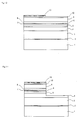
- Fig. 1 shows an example of a semiconductor laser device according to the present invention, which is a ridge-type laser device of an SCH (Separate Confinement Heterostructure).
- Reference number 1 denotes a single-crystal sapphire substrate
- 2 denotes a GaN (or AlN) layer formed at a low temperature
- 3 denotes an n-type GaN layer
- 4 denotes an n-type Al 0.1 Ga 0.9 N layer
- 5 denotes an n-type GaN layer
- 6 denotes an active layer mainly composed of In GaN
- 7 denotes a p-type Al 0.2 Ga 0.8 N layer
- 8 denotes a p-type GaN layer
- 9 denotes a p-type Al 0.1 Ga 0.9 N layer
- 10 denotes a p-type GaN layer doped with a group-II-impurity such as Mg
- 14 denotes an n-side electrode
- 13 and 15
- the n-type GaN layer 5 and p-type GaN layer 8 are waveguide layers for guiding the light emitted from the active layer.
- the p-type Al 0.2 Ga 0.8 N layer 7 is a barrier layer for further enhancing the confinement of injected carriers (particularly, electrons).
- the n-type Al 0.1 Ga 0.9 N layer 4 and p-type Al 0.1 Ga 0.9 N layer 9 are cladding layers with a refractive index lower than that of the waveguide layers 5 and 8, which confine the ewitted light into the waveguide layers duo to the difference in refractive indexes.
- the ridge portion 18 is formed so as to produce a step in effective refractive index along the lateral direction generated by a change in the thickness of the cladding layer on the waveguide layer, and thereby laterally confining the emitted light.
- the n-type GaN ground layer 3 provides a current path for device on an electrically insulating substrate.
- the low-temperature-grown GaN (or AlN) layer 2 is a so-called buffer layer, which is disposed so as to provide a smooth film on a sapphire substrate which is a dissimilar material to GaN.
- a nitride semiconductor laser according to the present invention comprises a plurality of laminated crystal layers 2 to 10 made of a group III nitride semiconductor (Al x Ga 1-x ) 1-y In y N (0 ⁇ x ⁇ 1, 0 ⁇ y ⁇ 1) and metal electrode 15 formed on the outermost layer.
- group III nitride semiconductor Al x Ga 1-x
- metal electrode 15 formed on the outermost layer.
- the contact layer 10 contains a high-impurity-concentration layer 10c held between a first outermost layer 10a close to a p-side electrode and a second outermost layer 10b close to an active layer.
- the thin high-impurity-concentration crystal layer 10c having a thickness of 0 to 100 ⁇ has a group-II-impurity concentration larger than the concentration of a group-II-impurity such as Mg or the like contained in the crystal layers 10a and 10b.
- polarization induced by the piezoelectric effect of GaN-related semiconductor crystal further reduces the schottky barrier height.
- the high-impurity-concentration layer 10c is formed to determine the polarity of the GaN-related crystal grown thereon.
- the insertion of the high-impurity-concentration layer 10c flips the polarity of the layer 10a grown thereon from that of the second outermost layer 10b so as to invert the direction of produced piezoelectric polarization.
- the first outermost layer 10a close to the p-side electrode is formed to have a the growth orientation of ⁇ 000-1>
- the second outermost 10b has a growth orientation of ⁇ 0001>.
- the thermal expansion coefficient of the sapphire substrate 1 is larger than that of GaN-based semiconductor crystal.
- the GaN-based semiconductor crystal layers 2 to 10 grown on the sapphire substrate 1 are under strong in-plane compressive stress caused by the large temperature difference during the cooling stage after the crystal growth.
- this in-plane stress generates high carrier concentration at the metal/semiconductor interface and thereby reducing the Schottky barrier height.
- the crystal structure of GaN is referred to as the so-called "wurtzite type" and has a hexagonal crystal structure.
- the axis of the hexagonal prism is referred to as C axis or ⁇ 0001> axis.
- GaN film on a crystalline substrate made of sapphire or the like is generally grown as a crystal layer having its C axis normal to the primary plane substrate. Therefore, the C plane (a plane normal to the C axis) appears on the surface of the GaN film formed on the sapphire substrate.
- a GaN crystal does not have mirror-image symmetry to the C axis.
- single-crystal GaN film on a sapphire substrate can be grown with two polarities, i.e., +C and -C planes.
- the +C plane has a polarity in which one of four bonds of each Ga atom extetnds to the outside of the film and the remaining three bonds extetnd into the film.
- the -C plane has a polarity in which three bonds of each N atom extetnd into the film. Therefore, the +C plane may be referred to as a Ga (gallium) plane and the -C plane may be referred to as a N (nitrogen) plane.
- GaN crystal has two polarities (one is Ga polarity and the other is N polarity) greatly influences various characteristics of a GaN-based semiconductor crystal.
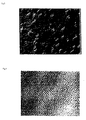
- the N polarity crystal is inferior in film surface flatness and easily causes a hexagonal protrusion as shown in Fig. 3.
- a smooth film is comparatively easily and reproducibly obtained and its surface flatness is far superior to that of N polarity film as shown in Fig. 4.
- the growing surface of a N polarity crystal easily captures a donor-like impurity such as oxygen.
- a p-type carrier concentration of up to only the order of a 10 17 cm -3 is obtained in the case of a film with N polarity.
- the Ga plane has advantages that a carrier concentration of up to 3 x 10 18 cm -3 is obtained and less oxygen impurities are captured.
- a semiconductor laser also serves as a waveguide device and has a stacked structure consisting of a number of layers having various refractive indexes. To reduce the wave-guiding loss due to scattering of light, it is necessary that the interface between layers constituting a device is sufficiently flat. From this point of view, it is impossible to fabricate a laser device having a preferable characteristic by using a crystal of N polarity.
- a GaN-based semiconductor layers are generally fabricated with Ga polarity of GaN crystal grown on sapphire substrate.
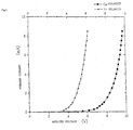
- Fig. 5 shows the voltage-current characteristic (denoted by ⁇ ) of the resultant GaN semiconductor laser of N polarity.
- the characteristic of a GaN semiconductor laser of Ga polarity (denoted by ⁇ ) is also shown in Fig. 5. From Fig. 5, it is found that the curve for the device of N polarity rises at much lower voltage. Since InGaN alloy consisting the junction has a band gap of approximately 3 eV, the turn-on voltage of the device is expected to be around 3 V. However, as shown in Fig. 5, current curve does not rise until the voltage reaches a point much higher than 3 V.
- the carrier concentration of the contact layer immediately below the p-side electrode is set to be 3 x 10 18 cm -3 , which is considered to be a sufficient value.
- the carrier concentration of a layer adjacent to the p-side electrode is equal to 1.5 x 10 17 cm -3
- the carrier concentration is lower than that of Ga polarity by one digit or more.
- a N polarity device exhibits superior contact characteristic and lower turn-on voltage. It is uncommon for other semiconductor materials that a contact with higher carrier concentration exhibits poorer characteristic whereas lower carrier concentration results in a device with lower contact resistivity. It is estimated that a strong piezoelectric characteristic of a GaN-based semiconductor causes such phenomenon.
- Piezoelectric effect is a phenomenon in which an electric polarization is induced by the stress applied to the crystal.
- a compressive strain occurs in the GaN film due to a difference between thermal expansion coefficients of the GaN film and the substrate.
- directions of generated polarization are changed when orientations of the crystal are changed (for example, direction is inverted).
- electrostatic polarization occurs in a semiconductor crystal, the distribution of carriers is modified from that in the absence of polarization.
- Fig. 6B is a schematic view showing an energy band structure in the vicinity of the p-side electrode of a laser device fabricated with GaN crystal assuming the absence of piezoelectricity.
- Fig. 6A is a schematic view showing an energy band structure in the vicinity of the p-side electrode of a laser device fabricated of a GaN crystal with Ga polarity.
- Fig. 6C is a schematic view showing an energy band structure in the vicinity of p-side electrode of a laser device fabricated with a GaN crystal of N polarity.
- the piezoelectric polarization has carriers (holes) move to counterbalance the electric field induced by the polarization itself.
- the carrier concentration in the vicinity of the electrode becomes lower than the case shown in Fig. 6B and the thickness of a Schottky barrier becomes larger than the case shown in Fig. 6B.
- a crystal layer with N polarity is superior in terms of p-side electrode characteristic alone but inferior in surface flatness as described above, and therefore, N polarity is difficult to be applied to laser devices. Moreover, though the reason is unknown yet, a crystal with N polarity usually has higher threading dislocation density and the luminous property is therefore generally inferior.
- the present invention provides a practical semiconductor laser by introducing the advantages of two crystal polarities of GaN. That is, the present invention introduces a high-impurity-concentration layer in the middle of the p-GaN film (contact layer) to invert the polarity of the outermost part of the film to N polarity and thereby improving the electrode characteristics without sacrificing flatness of the interfaces or luminous properties of the device.
- Formation of the high-impurity-concentration crystal layer is carried out by performing a growth step for forming said layer in which the concentration of Mg serving as an acceptor dopant is locally set at a very high value during the growth of p-GaN contact layer 10.
- concentration of Mg serving as an acceptor dopant is locally set at a very high value during the growth of p-GaN contact layer 10.
- Mg concentration of the p-GaN contact layer other than the portion where the polarity inversion takes place is kept in the range of 1 x 10 19 to 1 x 10 20 cm -3 . Unless the Mg concentration is kept in the above range, a value of 10 17 cm -3 or more is not obtained as the carrier concentration of p-GaN electrical characteristics of a device cannot be sufficiently improved.
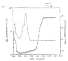
- Fig. 7 shows an SIMS (Secondary Ion Mass Spectrometry) results taken from the vicinity of the surface of a laser wafer according to the present invention.
- SIMS Secondary Ion Mass Spectrometry
- the depth of about 0.2 ⁇ m corresponds to the interface between p-GaN contact layer and p-AlGaN cladding layer.
- the Mg concentration of the portion corresponding to the increased Mg supply reaches 6 x 10 20 cm -3 .
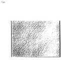
- Fig. 8 is a differential interference microphotograph showing the crystal surface of the contact layer of the wafer.
- the surface is somewhat smoother than that of the N polarity film shown in Fig.3, but exhibits a scale-like feature.
- the scale-like surface morphology imparts the depth resolution of the SIMS profile shown in Fig. 7.
- oxygen was detected with a concentration of approximately 1.5 x 10 18 cm -3 in the surface-side layers including the high-impurity-concentration layer.
- the Oxygen concentration was kept below the background level in other layers. Judging from these facts, the polarity of the upper layers are invented from Ga polarity to N polarity.
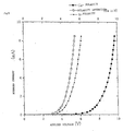
- Fig. 9 shows the current-voltage characteristic (denoted by ⁇ ) of a device fabricated from the wafer with the inversion from Ga polarity to N polarity. For comparison, Fig. 9 also shows the characteristic of a normal laser device with Ga polarity (denoted by ⁇ ) and that of a N polarity device (denoted by ⁇ ).
- the device with polarity inversion exhibits a slightly better characteristic than that of the device with N polarity. This is probably because the second outermost layer in the device with polarity inversion has higher carrier concentration and thus lower resistivity than the outermost layer next to the p-side electrode of the N e polarity device.
- the polarity inversion can be obtained even with a minute thickness(100 ⁇ or less, down to the order of monolayer) of high-impurity-concentration layer inserted into the contact layer. Moreover, a high-impurity-concentration layer has a low carrier concentration, it is desirable that the thickness of the layer be small from the viewpoint of electric conductivity.
- the high-impurity-concentration layer on the surface of a wafer, only makes the device operating voltage higher. This is because the high-impurity-concentration layer itself has a low carrier concentration and is similar to an insulator and thereby increasing the thickness of the barrier at the metal/semiconductor inter face.
- the step of fabricating the laser device of the above embodiment including the step of forming a high-impurity-concentration layer is described below in detail.
- a sapphire substrate 1 is set in an MOCVD reactor and held in a hydrogen-gas flow at a temperature of 1050° C and a pressure of 300 Torr to thermally clean the surface of the sapphire substrate 1. Then, the sapphire substrate 1 is cooled until its temperature reaches 600° C, ammonia (NH 3 ) serving as a nitrogen precursor and TMA (trimethylaluminum) serving as Al precursor are introduced into the reactor to deposit a buffer layer 2 made of AlN up to a thickness of 20 nm.
- NH 3 ammonia
- TMA trimethylaluminum
- TMA trimethylgallium
- Me-SiH 3 methyl silane
- an n-type AlGaN cladding layer 4 is formed by introducing TMA.
- the supply of TMA is stopped to grow an n-type GaN guide layer 5 up to 0.1 ⁇ m.
- supply of TMG and Me-SiH 3 is stopped and cooling is started to lower the substrate temperature to 750° C.
- carrier gas is changed from hydrogen to nitrogen.
- an active layer 6 is grown by introducing TMG, TMI, and Me-SiH 3 .
- TMG, TMI, and Me-SiH 3 are stopped and carrier gas is changed from nitrogen to hydrogen.
- the substrate temperature is raised to 1050° C again to form a p-type AlGaN layer 7 up to 0.01 ⁇ m by introducing TMG, TMA, and Et-Cp 2 Mg (ethyl-biscyclopentadienyl magnesium) as precursor of Mg which serves as a p-type impurity.
- the supply of TMA is stopped, a p-type GaN guide layer 8 is grown to 0.1 ⁇ m, and then a p-type AlGaN cladding layer 9 is grown to 0.5 ⁇ m by introducing TMA again.
- a second outermost layer 10b made of p-GaN (set Mg concentration: 4 x 10 19 cm -3 ) is grown to approximately 0.1 ⁇ m on the cladding layer 9. Then, the supply amount of Et-Cp 2 Mg is increased up to ten times of that in the provious step, while the supply amount of TMG as a Ga material is decreased to 1/2, and this state is kept for a period corresponding to a film thickness of 100 ⁇ to form a high-impurity-concentration layer 10c.
- the first outermost layer 10a is formed with a thickness of approximately 0.1 ⁇ m, and thus a p-type GaN contact layer 10 having a total thickness of 0.2 ⁇ m is formed to complete the wafer.
- a Ni (nickel) film 15 is formed as a p-side electrode on the p-type layer by vacuum evaporation.
- a p-side mesa, a current path structure for n-side electrode, and then a ridge shaped portion on the p-side mesa are fabricated on the wafer.
- the ridge shaped portion serves as a refractive-index-waveguide and also confines the injected current.
- the formation of the current path for the n-side electrode is performed first by partially removing the Ni film and then by etching the exposed nitride layer using reactive ion etching(RIE) with Cl 2 (chlorine) gas utilizing the Ni film as a mask. At this time, etching is performed up to a depth at which the n-type cladding layer 4 is slightly left to form a bottom portion 201 of the mesa structure.
- RIE reactive ion etching
- the Ni film is removed by wet etching while leaving a Ni film stripe 15 having a width of 5 ⁇ m.
- portions other than the portion immediately below the 5 ⁇ m-wide stripe portion, that is, the contact layer 10 and p-type AlGaN cladding layer 9 are removed while leaving approximately 0.1 ⁇ m of the cladding layer 9 by reactive ion etching (RIE) using the Ni stripe 15 as a mask to form a narrow ridge structure 18 as shown in Fig 13.
- RIE reactive ion etching
- a SiO 2 protective film is deposited on the above wafer by sputtering or the like.
- a 3 ⁇ m-wide window on the p-type ridge portion and a window portion on the n-side electrode are formed the SiO 2 protective film by a normal photolithography.
- Ti (titanium) with a thickness of 50 nm is evaporated onto a portion where the n-type GaN layer 3 is exposed and then, Al (aluminum) with a thickness of 200 nm is deposited on the portion to form an n-side electrode 14.
- Ni (nickel) with a thickness of 50 nm is evaporated onto the top of the p-side mesa and then Au (gold) with a thickness of 200 nm is deposited to form a p-side electrode 13.
- Au gold
Landscapes
- Physics & Mathematics (AREA)
- Condensed Matter Physics & Semiconductors (AREA)
- General Physics & Mathematics (AREA)
- Electromagnetism (AREA)
- Optics & Photonics (AREA)
- Semiconductor Lasers (AREA)
- Electrodes Of Semiconductors (AREA)
Abstract
Description
Claims (16)
- A nitride semiconductor laser comprising; a substrate; a plurality of crystal layers made of a group III nitride semiconductor (AlxGa1-x)1-yInyN (0≦x<1, 0≦y≦1) and laminated on the substrate in order; and a metallic electrode formed on an outermost layer of the crystal layers, wherein a crystal layer for holding the outermost layer together with the metallic electrode is a high-impurity-concentration crystal layer and the high-impurity-concentration crystal layer contains group II impurities having a concentration higher than concentrations of group II impurities of a crystal layer immediately below the high-impurity-concentration crystal layer and the outermost layer.
- A nitride semiconductor laser according to claim 1, wherein a growth orientation of the crystal layer grown from the substrate is inverted by forming the high-impurity-concentration crystal layer.
- A nitride semiconductor laser according to claim 1, wherein a main growth orientation of the crystal layer immediately below the high-impurity-concentration crystal layer is substantially <0001> direction and a crystal growth orientation is inverted to substantially <000-1> direction by forming the high-impurity-concentration crystal layer.
- A nitride semiconductor laser according to claim 1, wherein a position of the high-impurity-concentration crystal layer for inverting a growth orientation is in the middle of a p-GaN contact layer immediately below a p-side metallic electrode.
- A nitride semiconductor laser according to claim 1, wherein the substrate applies an in-plane compressive stress to the outermost layer.
- A nitride semiconductor laser according to claim 1, wherein the substrate is made of sapphire.
- A nitride semiconductor laser according to claim 1, wherein the group-II-impurity is Mg and the concentration of Mg of the high-impurity-concentration crystal layer exceeds 2 x 1020 cm-3.
- A nitride semiconductor laser according to claim 7, wherein Mg concentrations in the outermost layer immediately on the high-impurity-concentration crystal layer and a crystal layer immediately below the high-impurity-concentration crystal layer are kept in a range of 1 x 10¹⁹ to 1 x 1020 cm-3.
- A nitride semiconductor laser according to claim 7, wherein Mg concentrations of the outermost layer immediately on the high-impurity-concentration crystal layer and a crystal layer immediately below the high-impurity-concentration crystal layer are substantially the same.
- A fabrication method of a nitride semiconductor laser having a plurality of crystal layers made of group III nitride semiconductor (AlxGa1-x)1-yInyN (0≦x≦1, 0≦y≦1), comprising the steps of:forming a plurality of crystal layers with a substantially constant growth orientation;forming a high-impurity-concentration crystal layer having a group-II-impurity concentration higher than the group-II-impurity concentration of the crystal layer immediately below the high-impurity-concentration crystal layer;forming an outermost layer of crystal layers having a group-II-impurity concentration lower than the group-II-impurity concentration of the high-impurity-concentration crystal layer; andforming a metallic electrode on the outermost layer of the crystal layers.
- A fabrication method according to claim 10, wherein the crystal layers are formed by metal-organic chemical vapor deposition.
- A fabrication method according to claim 10, wherein, up to a crystal layer immediately below, the high-impurity-concentration crystal layer is grown by setting a main growth orientation to substantially <0001> direction, the high-impurity-concentration crystal layer forming step is included, and the growth orientation of crystal is inverted to substantially <000-1> direction in the vicinity of the high-impurity-concentration crystal layer.
- A fabrication method according to claim 10, wherein the substrate is made of sapphire.
- A fabrication method according to claim 10, wherein the group-II-impurity is Mg and the concentration of the high-impurity-concentration crystal layer exceeds 2 x 1020 cm-3.
- A fabrication method according to claim 14, wherein Mg concentrations of the outermost layer immediately on the high-impurity-concentration crystal layer and a crystal layer immediately below the high-impurity-concentration crystal layer are kept in a range of 1 x 10¹⁹ to 1 x 1020 cm-3.
- A fabrication method according to claim 14, wherein Mg concentrations of the outermost layer immediately on the high-impurity-concentration crystal layer and a crystal layer immediately below the high-impurity-concentration crystal layer are substantially the same.
Applications Claiming Priority (2)
| Application Number | Priority Date | Filing Date | Title |
|---|---|---|---|
| JP33023899A JP2001148532A (en) | 1999-11-19 | 1999-11-19 | Nitride semiconductor laser and manufacturing method therefor |
| JP33023899 | 1999-11-19 |
Publications (2)
| Publication Number | Publication Date |
|---|---|
| EP1104947A2 true EP1104947A2 (en) | 2001-06-06 |
| EP1104947A3 EP1104947A3 (en) | 2004-04-14 |
Family
ID=18230415
Family Applications (1)
| Application Number | Title | Priority Date | Filing Date |
|---|---|---|---|
| EP00124325A Withdrawn EP1104947A3 (en) | 1999-11-19 | 2000-11-16 | Nitride semiconductor laser and method for fabricating the same |
Country Status (2)
| Country | Link |
|---|---|
| EP (1) | EP1104947A3 (en) |
| JP (1) | JP2001148532A (en) |
Cited By (1)
| Publication number | Priority date | Publication date | Assignee | Title |
|---|---|---|---|---|
| US7613219B2 (en) | 2002-12-20 | 2009-11-03 | Cree, Inc. | Semiconductor devices having self aligned semiconductor mesas and contact layers |
Families Citing this family (8)
| Publication number | Priority date | Publication date | Assignee | Title |
|---|---|---|---|---|
| JP5093740B2 (en) * | 2001-07-26 | 2012-12-12 | 株式会社Ihi | Semiconductor crystal film growth method |
| US7462882B2 (en) | 2003-04-24 | 2008-12-09 | Sharp Kabushiki Kaisha | Nitride semiconductor light-emitting device, method of fabricating it, and semiconductor optical apparatus |
| JP2004327655A (en) * | 2003-04-24 | 2004-11-18 | Sharp Corp | Nitride semiconductor laser device, method of manufacturing the same, and semiconductor optical device |
| JP4647286B2 (en) * | 2004-11-09 | 2011-03-09 | 株式会社光波 | Semiconductor device and manufacturing method thereof |
| JP2008219059A (en) * | 2005-06-29 | 2008-09-18 | National Institute Of Advanced Industrial & Technology | ZnO light emitting device |
| JP2007043109A (en) * | 2005-06-29 | 2007-02-15 | National Institute Of Advanced Industrial & Technology | ZnO device |
| JP2009099798A (en) * | 2007-10-17 | 2009-05-07 | Toshiba Corp | Nitride semiconductor and manufacturing method thereof |
| JP7005890B2 (en) * | 2016-10-14 | 2022-01-24 | 株式会社リコー | Semiconductor light emitting elements, lighting devices, headlights, moving objects, illumination devices, video devices, projection type video devices and projectors. |
Family Cites Families (3)
| Publication number | Priority date | Publication date | Assignee | Title |
|---|---|---|---|---|
| KR19990014304A (en) * | 1997-07-30 | 1999-02-25 | 아사구사 나오유끼 | Semiconductor laser, semiconductor light emitting device and manufacturing method thereof |
| JPH11251685A (en) * | 1998-03-05 | 1999-09-17 | Toshiba Corp | Semiconductor laser |
| WO1999046822A1 (en) * | 1998-03-12 | 1999-09-16 | Nichia Chemical Industries, Ltd. | Nitride semiconductor device |
-
1999
- 1999-11-19 JP JP33023899A patent/JP2001148532A/en active Pending
-
2000
- 2000-11-16 EP EP00124325A patent/EP1104947A3/en not_active Withdrawn
Cited By (3)
| Publication number | Priority date | Publication date | Assignee | Title |
|---|---|---|---|---|
| US7613219B2 (en) | 2002-12-20 | 2009-11-03 | Cree, Inc. | Semiconductor devices having self aligned semiconductor mesas and contact layers |
| US7642626B2 (en) | 2002-12-20 | 2010-01-05 | Cree, Inc. | Semiconductor devices including mesa structures and multiple passivation layers |
| CN1729600B (en) * | 2002-12-20 | 2010-05-26 | 克里公司 | Semiconductor device with self-aligned semiconductor platform and contact layer and method of manufacturing related device |
Also Published As
| Publication number | Publication date |
|---|---|
| JP2001148532A (en) | 2001-05-29 |
| EP1104947A3 (en) | 2004-04-14 |
Similar Documents
| Publication | Publication Date | Title |
|---|---|---|
| JP3372226B2 (en) | Nitride semiconductor laser device | |
| US6920166B2 (en) | Thin film deposition method of nitride semiconductor and nitride semiconductor light emitting device | |
| US6586774B2 (en) | Method for fabricating nitride semiconductor, method for fabricating nitride semiconductor device, and nitride semiconductor device | |
| US7339195B2 (en) | Semiconductor light emitting device, its manufacturing method, semiconductor device and its manufacturing method | |
| US7083996B2 (en) | Nitride semiconductor device and manufacturing method thereof | |
| US6201823B1 (en) | Gallium nitride based compound semiconductor laser and method of forming the same | |
| US6690700B2 (en) | Nitride semiconductor device | |
| US20040213309A9 (en) | Nitride semiconductor layer structure and a nitride semiconductor laser incorporating a portion of same | |
| US20040159848A1 (en) | Nitride-based semiconductor laser device and method for the production thereof | |
| JP2006173621A (en) | Semiconductor laser | |
| JPH11191659A (en) | Method for growing nitride semiconductor and nitride semiconductor device | |
| JP3446660B2 (en) | Nitride semiconductor light emitting device | |
| US7867798B2 (en) | Semiconductor laser, method of manufacturing semiconductor laser, optical pickup and optical disk system | |
| US7816696B2 (en) | Nitride semiconductor device and method for manufacturing same | |
| US7755101B2 (en) | Semiconductor light emitting device | |
| JP2001148532A (en) | Nitride semiconductor laser and manufacturing method therefor | |
| JP3329753B2 (en) | Nitride semiconductor laser device | |
| JP2001044570A (en) | Nitride semiconductor laser device | |
| JP4628651B2 (en) | Manufacturing method of nitride semiconductor light emitting device | |
| US20060043356A1 (en) | Semiconductor optical device having quantum well structure and its manufacturing method | |
| JP3424634B2 (en) | Nitride semiconductor laser device | |
| JP3438675B2 (en) | Method for growing nitride semiconductor | |
| JP4826052B2 (en) | Nitride semiconductor laser device | |
| JP2003258381A (en) | Method for forming nitride semiconductor layer and light emitting device including those layers | |
| JPH11191658A (en) | Nitride semiconductor device |
Legal Events
| Date | Code | Title | Description |
|---|---|---|---|
| PUAI | Public reference made under article 153(3) epc to a published international application that has entered the european phase |
Free format text: ORIGINAL CODE: 0009012 |
|
| AK | Designated contracting states |
Kind code of ref document: A2 Designated state(s): AT BE CH CY DE DK ES FI FR GB GR IE IT LI LU MC NL PT SE TR |
|
| AX | Request for extension of the european patent |
Free format text: AL;LT;LV;MK;RO;SI |
|
| PUAL | Search report despatched |
Free format text: ORIGINAL CODE: 0009013 |
|
| AK | Designated contracting states |
Kind code of ref document: A3 Designated state(s): AT BE CH CY DE DK ES FI FR GB GR IE IT LI LU MC NL PT SE TR |
|
| AX | Request for extension of the european patent |
Extension state: AL LT LV MK RO SI |
|
| AKX | Designation fees paid | ||
| REG | Reference to a national code |
Ref country code: DE Ref legal event code: 8566 |
|
| STAA | Information on the status of an ep patent application or granted ep patent |
Free format text: STATUS: THE APPLICATION IS DEEMED TO BE WITHDRAWN |
|
| 18D | Application deemed to be withdrawn |
Effective date: 20041015 |