EP1102392A2 - Quadraturmodulator - Google Patents
Quadraturmodulator Download PDFInfo
- Publication number
- EP1102392A2 EP1102392A2 EP00125507A EP00125507A EP1102392A2 EP 1102392 A2 EP1102392 A2 EP 1102392A2 EP 00125507 A EP00125507 A EP 00125507A EP 00125507 A EP00125507 A EP 00125507A EP 1102392 A2 EP1102392 A2 EP 1102392A2
- Authority
- EP
- European Patent Office
- Prior art keywords
- signal
- switching device
- output
- output signal
- modulator
- Prior art date
- Legal status (The legal status is an assumption and is not a legal conclusion. Google has not performed a legal analysis and makes no representation as to the accuracy of the status listed.)
- Granted
Links
Images

Classifications
-
- H—ELECTRICITY
- H03—ELECTRONIC CIRCUITRY
- H03C—MODULATION
- H03C3/00—Angle modulation
- H03C3/38—Angle modulation by converting amplitude modulation to angle modulation
- H03C3/40—Angle modulation by converting amplitude modulation to angle modulation using two signal paths the outputs of which have a predetermined phase difference and at least one output being amplitude-modulated
Definitions
- the invention relates to a circuit arrangement for modulation with a transmit PLL.
- modulators are special suitable for GMSK modulation in mobile devices.
- Data transmission takes place in mobile radio devices based on the GSM standard using GMSK modulation.
- the same type of modulation is currently used for both voice transmission also used to transfer data.
- the data rate is however, for those going beyond the mere voice service Multimedia applications are not sufficient, so a newer 8-PSK modulation is standard.
- 8 PSK modulation three times the amount of data can be transmitted per unit of time.
- the GMSK symbols have a constant envelope, i.e. a constant amplitude, while the 8-PSK symbols have a not have constant envelope and different amplitude exhibit.
- the Combined transmission system is called GSM edge.
- a transmit PLL (PLL: Phase Lokked Loop) or upconversion loop is used for GMSK modulation.
- PLL Phase Lokked Loop
- a voltage controlled oscillator (VCO) will controlled with the phase information and generates the modulated Output signal for radiation via the antenna after suitable reinforcement.
- the output of the VCO is via a Down mixer to which the output signal of a channel oscillator is supplied, and a quadrature component modulator fed back a phase detector of the phase locked loop. in the The down-modulated signal with a phase detector Reference frequency compared.
- the output signal of the phase detector is passed through a loop filter to the frequency control signal to generate for the VCO.
- the quadrature component modulator is used at Irvine at al. from the mixed down Output signal driven.
- Yamawaki reference et al .: "A 2.7-V GSM RF Transceiver IC", IEEE Journal of Solid-State Circuits, Volume 32, No. 12, December 1997, p. 2089 - 2096 a transmit PLL is described in which the output of the down mixer unmodulated to an input of the phase detector is fed back and the other input of the phase detector from an oscillator to which the quadrature components of the useful signal are modulated, is fed.
- the Quadrature component modulator is in front of the phase discriminator either in the feedback loop of the transmit PLL (Irvine et al.) or in the reference signal path (Yamawaki et al.)
- the loop filter of the transmit PLL is a low pass and works in terms of radio frequency within the transmit PLL as a narrow-band Bandpass to let the useful signal pass.
- the VCO is low noise. This solution has become particularly special enforced because of a duplex filter after the transmit amplifier and be dispensed with immediately in front of the antenna can.
- the duplex filter attenuates the transmission signal outside the transmission band and prevents interference of noise and spurious emissions in the receiving channel. It is relatively expensive and requires increased power consumption in the transmitter amplifier.
- the object of the invention is a circuit arrangement to specify the modulation for two types of modulation, GMSK and 8-PSK modulation is particularly suitable.
- a circuit arrangement for Modulation comprising: a first modulator with a frequency controllable Oscillator that has an output for a first Has output signal; a phase detector, the output of the oscillator via a down mixer to the phase detector is fed back and a mixer arrangement to to provide a signal modulated with a useful signal; a second modulator on the input side with the output of the oscillator is connected and the one mixer arrangement comprises a signal modulated with the useful signal as provide second output signal; a first switching device, to between the first and the second output signal switch and a second switching device to an unmodulated one at an input terminal of the phase detector Provide signal when the first switching device is switched to the second output signal, and at the input terminal of the phase detector that of the useful signal Provide modulated signal when the first switching device is switched to the first output signal.
- the circuit arrangement according to the invention is for the GMSK modulation continues to use a transmit PLL and the the associated benefits are retained. If 8-PSK modulation is requested, the arrangement switches to one Direct modulator. As an oscillator for the carrier frequency of the Direct modulator, the VCO of the transmit PLL is used. For this the quadrature component modulator in the transmit PLL becomes ineffective switched.
- the arrangement combined according to the invention hence principles of transmit PLL and direct modulation, using particularly complex components together become.
- the standardization sees one lower specific transmission power lower noise requirements to the send path.
- the signal-to-noise ratio corresponding to the transmission power 6 dB lower than that of the GMSK modulation.
- the GMSK modulation after the power amplifier be filtered because of the noise in the transmission band through the nonlinear amplifier into the receiver band is folded (noise conversion gain).
- this effect only occurs very weak. It is therefore sufficient to use the output of the direct modulator and a surface wave filter in front of the transmission amplifier to be provided in order to avoid transmission into the receiving channel.
- a duplex filter that is used when using a direct modulator would have been necessary for GMSK modulation, is no longer necessary to meet the requirements of the GSM Edge standard to adhere to crosstalk attenuation with 8-PSK modulation.
- the GSMK path does not require a duplex filter, so that the Talk time of the mobile
- VCO of the transmit PLL as a synthesizer for the direct modulator sets for the direct modulator low-noise input signal available.
- the quickly regulating one Synthesizer with the relatively wide loop filter ensures making sure that load pulling effects compared to conventional Channel synthesizers can occur on end frequency can be avoided in the arrangement according to the invention.
- the VCO is expediently the transmission PLL operated in a power saving mode so that the available Talk time of the mobile device is increased further.
- the power amplifier for the transmit PLL is known to work non-linear with delimiter characteristic because of the GMSK symbols have a constant envelope or amplitude.
- the transmission stage for the direct modulator in 8-PSK operation requires one Amplifier with a linear transmission characteristic, since the Envelope of the 8-PSK symbols or their amplitude is not constant is changeable.
- the summary of the transmission paths of the transmit PLL and direct modulator can, on the one hand, according to the Transmit amplifiers take place, one for the transmit PLL non-linear amplifier stage is to be provided for the direct modulator a linear amplifier stage.
- the transmission paths can be before the power output stage take place, the amplifier with respect to its Working point is switchable to run, so that non-linear and linear amplifier operation from a single Amplifier level depending on the type of modulation are executable.
- the transmission architecture according to the invention makes it possible to one for both GMSK and 8-PSK operation Optimized power consumption and manufacturing costs Realizing solution. Compatibility with previous ones integrated transmit PLL circuits can be guaranteed. This results in an effective double use of components.
- the system can easily run on dual-band mobile devices both the GSM standard and the PCN standard are sufficient, be expanded.
- the arrangement in Figure 1 shows a conventional transmit PLL (Upconversion Loop) 100 and a direct modulation arrangement 200 using a common oscillator.
- the transmit PLL 100 includes a voltage controllable oscillator (VCO) 101, whose output signal is GMSK-modulated during GMSK operation is.
- VCO voltage controllable oscillator
- the oscillator is connected via a down mixer 102 downstream low-pass filter 103 to a phase detector or Phase discriminator 104 fed back.
- the down mixer 102 is the frequency of the generated by another VCO 104 Send channel supplied so that the output signal of the transmit VCO 101 on different channels of the available GSM frequency band is tunable.
- the other input of the phase detector 104 is fed by an oscillator 105, the Output signal first passed through a divider 106 through 4 is generated, the quadrature components shifted by 0 ° / 90 °. These are assigned in the respective quadrature components Mixers 107 and 108 with the quadrature components I, Q modulated a useful signal.
- the modulated signals are added in a summer 109 and via a low-pass filter 110 forwarded the reference input of phase detector 104.
- the modulated applied to this input of the phase detector 104 Signal is with the path 102, ..., 104 compared transmitted signal.
- the phase difference is passed over a loop filter 111 and as frequency control information fed into the transmit VCO 101.
- the Loop filter 111 has low-pass characteristics and leaves that Frequency band of the useful signal through, so that the VCO 101 accordingly the transmission signal I, Q in phase becomes.
- the GMSK-modulated is then at the output of the VCO 101 Broadcast signal on.
- the direct modulator 200 has an 8-PSK modulation Quadrature component mixer 201, 202 on which the useful signal components I, Q are supplied.
- the mixers 201, 202 carrier signals phase-shifted from one another by 90 ° fed. For this the carrier frequency at the output of the VCO 101 of the transmit PLL and tapped in a phase shifter 203 split into quadrature components.
- a summator 204 adds the modulated quadrature components the outputs of the mixers 201, 202 to the 8-PSK-modulated output signal of the direct modulator.
- the quadrature components I, Q of the useful signal are at connections 301, 302 fed.
- a switch 303 connects the connections 301, 302 with the signal inputs of the mixers 107, 108 of the transmit PLL during GMSK operation.
- a switch 304 is used to connect the connections 301, 302 to the Useful signal inputs of mixers 201, 202 during 8-PSK operation.
- the switches 303, 304 are switched mutually. With switch 304 closed for 8 PSK operation the switch 303 flipped to connections 305, 306 at which a constant signal V is fed.
- the constant signal V must be so large for this can be chosen that the mixer 107, 108 as a pure amplifier work.
- the VCO 101 of the transmit PLL sets in this case Unmodulated carrier signal for direct modulator 200 ready.
- a surface wave filter at the output of the summing element 204 (OFW) 105 connected.
- the surface wave filter acts as a steep band pass that is outside the broadcast band horizontal signal components suppressed with high attenuation.
- the Attenuation of the SAW filter is sufficient to meet the specifications of the standard for 8-PSK operation. Across from GMSK, the transmission power at 8-PSK is 6 dB lower, so that an SAW filter is sufficient.
- the SAW filter is relative inexpensive and still provides sufficient Damping.
- the modulated output signal of the VCO 101 is by a Transmit amplifier 112 amplified.
- the amplifier 112 has one non-linear characteristic and is used in limiter operation, because the GMSK signal has a constant envelope.
- the SAW filter 205 as a transmission amplifier is a linear amplifier 206 downstream, so that the symbol-changing Amplitude information of an 8-PSK signal after amplification preserved.
- the outputs of both amplifiers 112, 206 are placed on a changeover switch 307 which, depending on the operating requirement between GMSK or 8 PSK modulated output signal toggles.
- the transmission signal is via an antenna 308 emitted.
- the circuit described is generally suitable for a Modulation switchable between GMSK and PSK in any Frequency.
- the circuit can therefore by parallel accordingly guided branches for both the GSM 900 mobile radio standard as well as for the mobile radio standard DCS 1800 or PCN become.
- the components described so far are dimensioned for GSM 900.
- For the PCN frequency band is parallel for VCO 101 a VCO 113 with a downstream amplifier 114 provided.
- Parallel to the direct modulator 201, 202 is for the PCN frequency band a quadrature component modulator 207, 208 and a corresponding SAW filter on the output side 209 and an associated amplifier 210.
- the signal paths are merged in the switch 307.
- a multiplexer 211 ensures a switchover at the input of phase shifter 203 between VCOs 101 and 113.
- the described Circuit is suitable for manufacturing a dual-band mobile device with GSM edge capability.
- Integrated circuit 10 is a conventional component for a transmit PLL for GMSK modulation is available.
- the rimmed with 20 Components of the direct modulator can be integrated in one further integrated circuit can be manufactured. there is the circuit 20 connection compatible to the already known Circuit 10.
- a GMSK / 8-PSK-capable mobile device can therefore using the previous circuit architecture for a GMSK-capable mobile device can be developed by essentially only the integrated circuit 20 and the Components 205, 206, 209, 210 and 307 can be added.
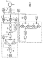
- the 8 PSK operation is the Quadrature component modulator 107, 108 bypassed.
- a changeover switch at the output of the divider 106 120 is provided, which in GSM operation is that of the oscillator 105 switches the generated carrier frequency to the modulator 107, 108, with 8-PSK operation, however, via an amplifier 121 leads.
- the phase discriminator 104 At the input of the phase discriminator 104 provides a Switch 122 for a corresponding switchover of the signal path.
- This solution has the advantage that the mixers 107, 108 can be switched off with 8-PSK operation. This will Power loss saved, the batteries of the mobile device are spared and the available speaking time of the device extended.
- Switches 303, 304 are no longer required.
- the circuit in FIG. 2 has amplifier amplifiers for GMSK and 8-PSK operation combined power amplifiers (each for GSM and PCN standard separately).
- the amplifier 123 is both for limiter operation during GMSK modulation as also for linear amplifier operation during 8-PSK modulation switchable and on the input side via a switch 124 with both the output of the VCO 101 and the output of SAW filter 205 connected.
- the board layout, as well as the Wiring effort and the routing of the high-frequency signals are simplified.
- the VCOs 101, 113 are expedient with respect to their Driver capability and thus power loss can be switched. With GMSK operation, VCOs 101, 113 become high Power consumption operated to match a signal sufficient driver capability for amplifiers 112 and 114 available. For 8-PSK operation, however, it is sufficient the VCOs 101, 113 with low driver capability and therefore to operate correspondingly lower power consumption because mixers 201, 202 and 207, 208 have sufficient driver power provide for the assigned power amplifiers 206 and 210. The battery capacity and available transmission time with 8 PSK operation this in turn increases.
- Switching between the modulation types GMSK and 8-PSK is controlled by a switching signal S.
- the signal S becomes the switches, the amplifiers and the oscillators that are related Linearity behavior or driver power switchable are fed.
- the phase link 106 may be without connecting frequency division to the output of filter 103.
- the output of filter 110 is in the phase detector 104 fed back.
- the oscillator 105 is optionally with the interposition of a divider, i.e. without modulator, to the other connection of the phase detector 104 connected.
Landscapes
- Digital Transmission Methods That Use Modulated Carrier Waves (AREA)
- Transmitters (AREA)
- Transceivers (AREA)
Abstract
Description
- Figur 1
- ein erstes Ausführungsbeispiel für eine Anordnung zur umschaltbaren GMSK-/8-PSK-Modulation und
- Figur 2
- ein zweites Ausführungsbeispiel für eine solche Anordnung.
Claims (9)
- Schaltungsanordnung zur Modulation, die umfaßt:einen ersten Modulator (100) miteinem frequenzsteuerbaren Oszillator (101, 113), der einen Ausgang für ein erstes Ausgangssignal aufweist,einem Phasendetektor (104), wobei der Ausgang des Oszillators (101, 113) über einen Abwärtsmischer (102) auf den Phasendetektor (104) rückgekoppelt ist undeiner Mischeranordnung (107, 108, 109), um ein mit einem Nutzsignal moduliertes Signal bereitzustellen,einen zweiten Modulator (200),der eingangsseitig mit dem Ausgang des Oszillators (101, 113) verbunden ist undder eine Mischeranordnung (201, 202, 204, 207, 208) umfaßt, um ein mit dem Nutzsignal moduliertes Signal als zweites Ausgangssignal bereitzustellen,eine erste Umschalteinrichtung (307), um zwischen dem ersten und dem zweiten Ausgangssignal umzuschalten undeine zweite Umschalteinrichtung (303, 120, 122), um an einem Eingangsanschluß des Phasendetektors (104) ein nicht moduliertes Signal bereitzustellen, wenn die erste Umschalteinrichtung (307) auf das zweite Ausgangssignal umgeschaltet ist, und um am Eingangsanschluß des Phasendetektors (104) das vom Nutzsignal modulierte Signal bereitzustellen, wenn die erste Umschalteinrichtung (307) auf das erste Ausgangssignal umgeschaltet ist.
- Schaltungsanordnung nach Anspruch 1,
dadurch gekennzeichnet, daß
Anschlüsse (301, 302) zur Eingabe von Quadraturkomponenten (I, Q) des Nutzsignals vorgesehen sind und eine Schalteinrichtung (304) und Anschlüsse (305, 306) für ein Konstantsignal (V), daßdie Schalteinrichtung (304) derart ausgebildet ist, daß das Nutzsignal der Mischeranordnung (201, 202, 204, 207, 208) des zweiten Modulators (200) zuführbar ist und daß die zweite Umschalteinrichtung (303) derart ausgebildet ist, daß das Konstantsignal (V) der zweiten Mischeranordnung (200) zuführbar ist, wenn die erste Umschalteinrichtung (307) auf das zweite Ausgangssignal umgeschaltet ist, und daßdie zweite Umschalteinrichtung (303) derart ausgebildet ist, daß das Nutzsignal der Mischeranordnung (107, 108, 109) des ersten Modulators (100) zuführbar ist, wenn die erste Umschalteinrichtung (307) auf das erste Ausgangssignal umgeschaltet ist. - Schaltungsanordnung nach Anspruch 1,
dadurch gekennzeichnet, daß
die zweite Umschalteinrichtung (120, 122) derart ausgebildet ist, daßdie Mischeranordnung (107, 108, 109) des ersten Modulators (100) eingangsseitig mit einem weiteren Oszillator (105) gekoppelt ist und ausgangsseitig mit dem Eingangsanschluß des Phasendetektors (104), wenn die erste Umschalteinrichtung (307) auf das erste Ausgangssignal umgeschaltet ist, und daßder Eingangsanschluß des Phasendetektors (104) mit dem weiteren Oszillator (105) unter Umgehung der Mischeranordnung (107, 108, 109) des ersten Modulators (100) gekoppelt ist, wenn die erste Umschalteinrichtung (307) auf das zweite Ausgangssignal umgeschaltet ist. - Schaltungsanordnung nach einem der Ansprüche 1 bis 3,
gekennzeichnet dadurch
einen nichtlinearen Verstärker (112, 114), über den das erste Ausgangssignal an die erste Umschalteinrichtung (307) koppelbar ist, und einen linearen Verstärker (206, 210), durch den das zweite Ausgangssignal an die erste Umschalteinrichtung (307) koppelbar ist. - Schaltungsanordnung nach einem der Ansprüche 1 bis 3,
gekennzeichnet dadurch
einen Verstärker (123), der zwischen einer ersten Betriebsart mit nichtlinearem Verstärkerbetrieb und einer zweiten Betriebsart mit linearem Verstärkerbetrieb umschaltbar ist, und einen Schalter (124), über den dem Verstärker (123) eingangsseitig das erste oder das zweite Ausgangssignal zuführbar ist. - Schaltungsanordnung nach einem der Ansprüche 1 bis 5,
gekennzeichnet dadurch
ein Oberflächenwellenfilter (205, 209), das dem Ausgang der Mischereinrichtung (201, 202, 204, 207, 208) des zweiten Modulators (200) nachgeschaltet ist. - Schaltungsanordnung nach Anspruch 1 oder 2,
dadurch gekennzeichnet, daß
die Mischeranordnung (107, 108, 109) des ersten Modulators (100) eingangsseitig mit dem Abwärtsmischer (102) gekoppelt ist. - Schaltungsanordnung nach einem der Ansprüche 1 bis 7,
dadurch gekennzeichnet, daß
der Oszillator (101, 113) eine Betriebsart mit hoher Treiberfähigkeit und eine Betriebsart mit niedrigerer Treiberfähigkeit hat und daß die zweite Betriebart einstellbar ist, wenn die erste Umschalteinrichtung (307) auf das zweite Ausgangssignal umgeschaltet ist. - Schaltungsanordnung nach einem der Ansprüche 1 bis 8,
dadurch gekennzeichnet, daß
das Nutzsignal in Form von Quadraturkomponenten (I, Q) zuführbar ist und die Modulatoren jeweils aufweisen:ein Phasenglied (106, 203) zur Aufspaltung eines Trägersignals in um 90° zueinander phasenverschobene Signalkomponenten,zwei Mischer (107, 201, 207; 108, 202, 208), denen jeweils eine der Signalkomponenten und eine der Quadraturkomponenten zuführbar ist, undein Summierglied (109, 204) zur Addition von Ausgangssignalen der Mischer.
Applications Claiming Priority (2)
| Application Number | Priority Date | Filing Date | Title |
|---|---|---|---|
| DE19956073 | 1999-11-22 | ||
| DE19956073A DE19956073C2 (de) | 1999-11-22 | 1999-11-22 | Modulationsanordnung |
Publications (3)
| Publication Number | Publication Date |
|---|---|
| EP1102392A2 true EP1102392A2 (de) | 2001-05-23 |
| EP1102392A3 EP1102392A3 (de) | 2003-01-02 |
| EP1102392B1 EP1102392B1 (de) | 2004-03-24 |
Family
ID=7929873
Family Applications (1)
| Application Number | Title | Priority Date | Filing Date |
|---|---|---|---|
| EP00125507A Expired - Lifetime EP1102392B1 (de) | 1999-11-22 | 2000-11-21 | Quadraturmodulator |
Country Status (3)
| Country | Link |
|---|---|
| US (1) | US6369666B1 (de) |
| EP (1) | EP1102392B1 (de) |
| DE (2) | DE19956073C2 (de) |
Cited By (4)
| Publication number | Priority date | Publication date | Assignee | Title |
|---|---|---|---|---|
| WO2003088511A1 (en) * | 2002-04-05 | 2003-10-23 | Telefonaktiebolaget Lm Ericsson (Publ) | Multimodulation transmitter |
| WO2007037963A1 (en) * | 2005-09-26 | 2007-04-05 | Nxp B.V. | Edge transceiver architecture and related methods |
| RU2316889C1 (ru) * | 2006-06-20 | 2008-02-10 | Федеральное государственное образовательное учреждение высшего профессионального образования "Морской государственный университет имени адмирала Г.И. Невельского" | Частотный детектор радиоэлектронной аппаратуры |
| US7697901B2 (en) | 2005-09-26 | 2010-04-13 | St-Ericsson Sa | Digital variable gain mixer |
Families Citing this family (10)
| Publication number | Priority date | Publication date | Assignee | Title |
|---|---|---|---|---|
| EP1107530B1 (de) * | 1999-12-07 | 2007-02-28 | Motorola Semiconducteurs S.A. | Rahmenformat für Radio Nachrichtenübertragungssystem |
| US6970681B2 (en) * | 2001-11-14 | 2005-11-29 | Broadcom, Corp. | Integrated multimode radio and components thereof |
| DE10209516A1 (de) * | 2002-03-04 | 2003-07-17 | Infineon Technologies Ag | Sendeanordnung |
| JP2005072031A (ja) * | 2003-08-22 | 2005-03-17 | Renesas Technology Corp | 高周波用半導体装置および通信用電子部品並びに無線通信システム |
| US7719376B2 (en) * | 2003-12-04 | 2010-05-18 | St-Ericsson Sa | Avoidance of discontinuities when switching between modulation schemes |
| US7362820B2 (en) * | 2005-05-18 | 2008-04-22 | Motorola, Inc. | Apparatus and method for modulating and digitally predistorting a signal in a multiple modulation schemes |
| US8428212B2 (en) * | 2008-01-30 | 2013-04-23 | Intel Mobile Communications GmbH | Frequency synthesis using upconversion PLL processes |
| US20090258610A1 (en) * | 2008-04-15 | 2009-10-15 | Mediatek Inc. | Apparatus for multiple modulations with a transition mode in a baseband transmitter and method therefor |
| GB0808886D0 (en) * | 2008-05-15 | 2008-06-25 | Cambridge Silicon Radio Ltd | Dual purpose modulator |
| US11239990B2 (en) * | 2019-06-12 | 2022-02-01 | Infineon Technologies Ag | Phase error determination using two modulators |
Family Cites Families (4)
| Publication number | Priority date | Publication date | Assignee | Title |
|---|---|---|---|---|
| FR2742946B1 (fr) * | 1995-12-22 | 1998-01-16 | Alcatel Mobile Comm France | Terminal de radiocommunication multimode |
| EP0852448A1 (de) * | 1997-01-02 | 1998-07-08 | Nokia Mobile Phones Ltd. | Teilnehmer-Endgerät für mobile Kommunikationen |
| GB2348755B (en) * | 1999-04-01 | 2001-03-07 | Wireless Systems Int Ltd | Signal processing |
| US6246286B1 (en) * | 1999-10-26 | 2001-06-12 | Telefonaktiebolaget Lm Ericsson | Adaptive linearization of power amplifiers |
-
1999
- 1999-11-22 DE DE19956073A patent/DE19956073C2/de not_active Expired - Fee Related
-
2000
- 2000-11-21 EP EP00125507A patent/EP1102392B1/de not_active Expired - Lifetime
- 2000-11-21 DE DE50005781T patent/DE50005781D1/de not_active Expired - Lifetime
- 2000-11-22 US US09/718,895 patent/US6369666B1/en not_active Expired - Lifetime
Cited By (7)
| Publication number | Priority date | Publication date | Assignee | Title |
|---|---|---|---|---|
| WO2003088511A1 (en) * | 2002-04-05 | 2003-10-23 | Telefonaktiebolaget Lm Ericsson (Publ) | Multimodulation transmitter |
| CN100353675C (zh) * | 2002-04-05 | 2007-12-05 | 艾利森电话股份有限公司 | 多调制发射机 |
| US7469017B2 (en) | 2002-04-05 | 2008-12-23 | Telefonaktiebolaget Lm Ericsson (Publ) | Multimodulation transmitter |
| WO2007037963A1 (en) * | 2005-09-26 | 2007-04-05 | Nxp B.V. | Edge transceiver architecture and related methods |
| US7697901B2 (en) | 2005-09-26 | 2010-04-13 | St-Ericsson Sa | Digital variable gain mixer |
| US7720176B2 (en) | 2005-09-26 | 2010-05-18 | St-Ericsson Sa | Edge transceiver architecture and related methods |
| RU2316889C1 (ru) * | 2006-06-20 | 2008-02-10 | Федеральное государственное образовательное учреждение высшего профессионального образования "Морской государственный университет имени адмирала Г.И. Невельского" | Частотный детектор радиоэлектронной аппаратуры |
Also Published As
| Publication number | Publication date |
|---|---|
| EP1102392B1 (de) | 2004-03-24 |
| DE19956073C2 (de) | 2002-03-28 |
| US6369666B1 (en) | 2002-04-09 |
| DE50005781D1 (de) | 2004-04-29 |
| EP1102392A3 (de) | 2003-01-02 |
| DE19956073A1 (de) | 2001-05-31 |
Similar Documents
| Publication | Publication Date | Title |
|---|---|---|
| DE69837698T2 (de) | Multimodusfunkkommunikationssystem | |
| DE69812120T2 (de) | Doppelbandiger leistungsverstärker mit zwei betriebsarten | |
| DE69834875T2 (de) | Frequenzumsetzungsschaltung | |
| DE69735156T2 (de) | Multibandkommunikationsgerät | |
| DE69832705T2 (de) | Mehrfachmethodedirektmischempfänger | |
| DE4126080C2 (de) | Mischersystem für einen Direktumsetzungsempfänger | |
| DE69838382T2 (de) | Konfigurierbare integrierte Ein-Chip-Sende-/Empfangschaltung | |
| DE60034301T2 (de) | Vorwärtsgekoppelter Verstärker und Steuerschaltung dafür | |
| DE4480702C2 (de) | Leistungsverstärker mit einer Amplitudenmodulationssteuervorrichtung und einer damit verbundenen Phasenmodulationsvorrichtung | |
| DE69623426T2 (de) | Multimoden-Funkendgerät | |
| EP1102392B1 (de) | Quadraturmodulator | |
| DE60018440T2 (de) | Überlagerungsoszillator für hochfrequenzfunkgeräte | |
| DE102005058459A1 (de) | Sende-Empfangs-Vorrichtung und Modul | |
| DE3913593A1 (de) | Schaltungsanordnung zur umsetzung eines empfangenen modulierten informationssignals in ein zwischenfrequenzsignal | |
| DE69833184T2 (de) | Gerät in einem Kommunikationssystem | |
| DE19713102A1 (de) | Integrierte Empfangsschaltung für Mobiltelefon | |
| EP1481487B1 (de) | Sendeanordnung | |
| DE69801358T2 (de) | Frequenzwandlerschaltung für Kabelempfänger mit Modem | |
| EP1258077B1 (de) | Schaltungsanordnung zur direktmodulation | |
| DE102017002799B4 (de) | Drahtloser transceiver mit fernem front-end | |
| DE60017573T2 (de) | Wirksame GSM/GCS/UMTS (UTRA/FDD) Sende-Empfänger-Architektur | |
| DE60312252T2 (de) | Modulations- und Demodulationsvorrichtung und drathloses Kommunikationsgerät | |
| EP1203454B1 (de) | Modulator-demodulator | |
| EP1075739B1 (de) | Mit frequenzsprungtechnik arbeitendes digitales mehrteilnehmer-funk-nachrichtenübertragungssystem | |
| DE4430029C2 (de) | Funkgerät |
Legal Events
| Date | Code | Title | Description |
|---|---|---|---|
| PUAI | Public reference made under article 153(3) epc to a published international application that has entered the european phase |
Free format text: ORIGINAL CODE: 0009012 |
|
| AK | Designated contracting states |
Kind code of ref document: A2 Designated state(s): AT BE CH CY DE DK ES FI FR GB GR IE IT LI LU MC NL PT SE TR |
|
| AX | Request for extension of the european patent |
Free format text: AL;LT;LV;MK;RO;SI |
|
| PUAL | Search report despatched |
Free format text: ORIGINAL CODE: 0009013 |
|
| RIC1 | Information provided on ipc code assigned before grant |
Free format text: 7H 03D 3/00 A, 7H 03C 3/40 B, 7H 03C 3/09 B |
|
| AK | Designated contracting states |
Kind code of ref document: A3 Designated state(s): AT BE CH CY DE DK ES FI FR GB GR IE IT LI LU MC NL PT SE TR |
|
| AX | Request for extension of the european patent |
Free format text: AL;LT;LV;MK;RO;SI |
|
| GRAP | Despatch of communication of intention to grant a patent |
Free format text: ORIGINAL CODE: EPIDOSNIGR1 |
|
| 17P | Request for examination filed |
Effective date: 20030627 |
|
| AKX | Designation fees paid |
Designated state(s): DE FR GB |
|
| GRAS | Grant fee paid |
Free format text: ORIGINAL CODE: EPIDOSNIGR3 |
|
| GRAA | (expected) grant |
Free format text: ORIGINAL CODE: 0009210 |
|
| AK | Designated contracting states |
Kind code of ref document: B1 Designated state(s): DE FR GB |
|
| REG | Reference to a national code |
Ref country code: GB Ref legal event code: FG4D Free format text: NOT ENGLISH |
|
| REG | Reference to a national code |
Ref country code: IE Ref legal event code: FG4D Free format text: GERMAN |
|
| REF | Corresponds to: |
Ref document number: 50005781 Country of ref document: DE Date of ref document: 20040429 Kind code of ref document: P |
|
| GBT | Gb: translation of ep patent filed (gb section 77(6)(a)/1977) |
Effective date: 20040527 |
|
| REG | Reference to a national code |
Ref country code: IE Ref legal event code: FD4D |
|
| ET | Fr: translation filed | ||
| PLBE | No opposition filed within time limit |
Free format text: ORIGINAL CODE: 0009261 |
|
| STAA | Information on the status of an ep patent application or granted ep patent |
Free format text: STATUS: NO OPPOSITION FILED WITHIN TIME LIMIT |
|
| 26N | No opposition filed |
Effective date: 20041228 |
|
| REG | Reference to a national code |
Ref country code: FR Ref legal event code: TP Owner name: INTEL MOBILE COMMUNICATIONS GMBH, DE Effective date: 20120404 Ref country code: FR Ref legal event code: CA Effective date: 20120404 |
|
| REG | Reference to a national code |
Ref country code: GB Ref legal event code: 732E Free format text: REGISTERED BETWEEN 20120607 AND 20120613 |
|
| REG | Reference to a national code |
Ref country code: GB Ref legal event code: 732E Free format text: REGISTERED BETWEEN 20121213 AND 20121219 |
|
| REG | Reference to a national code |
Ref country code: DE Ref legal event code: R081 Ref document number: 50005781 Country of ref document: DE Owner name: INTEL MOBILE COMMUNICATIONS GMBH, DE Free format text: FORMER OWNER: INFINEON TECHNOLOGIES AG, 85579 NEUBIBERG, DE Effective date: 20130315 Ref country code: DE Ref legal event code: R081 Ref document number: 50005781 Country of ref document: DE Owner name: INTEL MOBILE COMMUNICATIONS GMBH, DE Free format text: FORMER OWNER: INTEL MOBILE COMMUNICATIONS TECHNOLOGY GMBH, 85579 NEUBIBERG, DE Effective date: 20130326 Ref country code: DE Ref legal event code: R081 Ref document number: 50005781 Country of ref document: DE Owner name: INTEL MOBILE COMMUNICATIONS GMBH, DE Free format text: FORMER OWNER: INFINEON TECHNOLOGIES AG, 81669 MUENCHEN, DE Effective date: 20130314 Ref country code: DE Ref legal event code: R081 Ref document number: 50005781 Country of ref document: DE Owner name: INTEL MOBILE COMMUNICATIONS GMBH, DE Free format text: FORMER OWNER: INTEL MOBILE COMMUNICATIONS GMBH, 85579 NEUBIBERG, DE Effective date: 20130315 Ref country code: DE Ref legal event code: R081 Ref document number: 50005781 Country of ref document: DE Owner name: INTEL DEUTSCHLAND GMBH, DE Free format text: FORMER OWNER: INTEL MOBILE COMMUNICATIONS GMBH, 85579 NEUBIBERG, DE Effective date: 20130315 Ref country code: DE Ref legal event code: R081 Ref document number: 50005781 Country of ref document: DE Owner name: INTEL DEUTSCHLAND GMBH, DE Free format text: FORMER OWNER: INFINEON TECHNOLOGIES AG, 81669 MUENCHEN, DE Effective date: 20130314 Ref country code: DE Ref legal event code: R081 Ref document number: 50005781 Country of ref document: DE Owner name: INTEL DEUTSCHLAND GMBH, DE Free format text: FORMER OWNER: INFINEON TECHNOLOGIES AG, 85579 NEUBIBERG, DE Effective date: 20130315 Ref country code: DE Ref legal event code: R081 Ref document number: 50005781 Country of ref document: DE Owner name: INTEL DEUTSCHLAND GMBH, DE Free format text: FORMER OWNER: INTEL MOBILE COMMUNICATIONS TECHNOLOGY GMBH, 85579 NEUBIBERG, DE Effective date: 20130326 |
|
| PGFP | Annual fee paid to national office [announced via postgrant information from national office to epo] |
Ref country code: FR Payment date: 20141110 Year of fee payment: 15 Ref country code: GB Payment date: 20141119 Year of fee payment: 15 |
|
| REG | Reference to a national code |
Ref country code: DE Ref legal event code: R081 Ref document number: 50005781 Country of ref document: DE Owner name: INTEL DEUTSCHLAND GMBH, DE Free format text: FORMER OWNER: INTEL MOBILE COMMUNICATIONS GMBH, 85579 NEUBIBERG, DE |
|
| PGFP | Annual fee paid to national office [announced via postgrant information from national office to epo] |
Ref country code: DE Payment date: 20151118 Year of fee payment: 16 |
|
| REG | Reference to a national code |
Ref country code: FR Ref legal event code: CD Owner name: INTEL DEUTSCHLAND GMBH, DE Effective date: 20160126 |
|
| GBPC | Gb: european patent ceased through non-payment of renewal fee |
Effective date: 20151121 |
|
| REG | Reference to a national code |
Ref country code: FR Ref legal event code: ST Effective date: 20160729 |
|
| PG25 | Lapsed in a contracting state [announced via postgrant information from national office to epo] |
Ref country code: GB Free format text: LAPSE BECAUSE OF NON-PAYMENT OF DUE FEES Effective date: 20151121 |
|
| PG25 | Lapsed in a contracting state [announced via postgrant information from national office to epo] |
Ref country code: FR Free format text: LAPSE BECAUSE OF NON-PAYMENT OF DUE FEES Effective date: 20151130 |
|
| REG | Reference to a national code |
Ref country code: DE Ref legal event code: R119 Ref document number: 50005781 Country of ref document: DE |
|
| PG25 | Lapsed in a contracting state [announced via postgrant information from national office to epo] |
Ref country code: DE Free format text: LAPSE BECAUSE OF NON-PAYMENT OF DUE FEES Effective date: 20170601 |