EP1102160A2 - Synchroner Sender von digitalen Daten - Google Patents
Synchroner Sender von digitalen Daten Download PDFInfo
- Publication number
- EP1102160A2 EP1102160A2 EP00310193A EP00310193A EP1102160A2 EP 1102160 A2 EP1102160 A2 EP 1102160A2 EP 00310193 A EP00310193 A EP 00310193A EP 00310193 A EP00310193 A EP 00310193A EP 1102160 A2 EP1102160 A2 EP 1102160A2
- Authority
- EP
- European Patent Office
- Prior art keywords
- data
- buffer
- rate
- response
- source
- Prior art date
- Legal status (The legal status is an assumption and is not a legal conclusion. Google has not performed a legal analysis and makes no representation as to the accuracy of the status listed.)
- Granted
Links
Images
Classifications
-
- H—ELECTRICITY
- H04—ELECTRIC COMMUNICATION TECHNIQUE
- H04L—TRANSMISSION OF DIGITAL INFORMATION, e.g. TELEGRAPHIC COMMUNICATION
- H04L49/00—Packet switching elements
- H04L49/90—Buffering arrangements
- H04L49/9063—Intermediate storage in different physical parts of a node or terminal
- H04L49/9078—Intermediate storage in different physical parts of a node or terminal using an external memory or storage device
-
- H—ELECTRICITY
- H04—ELECTRIC COMMUNICATION TECHNIQUE
- H04L—TRANSMISSION OF DIGITAL INFORMATION, e.g. TELEGRAPHIC COMMUNICATION
- H04L49/00—Packet switching elements
- H04L49/90—Buffering arrangements
-
- H—ELECTRICITY
- H04—ELECTRIC COMMUNICATION TECHNIQUE
- H04L—TRANSMISSION OF DIGITAL INFORMATION, e.g. TELEGRAPHIC COMMUNICATION
- H04L12/00—Data switching networks
- H04L12/54—Store-and-forward switching systems
- H04L12/56—Packet switching systems
- H04L12/5601—Transfer mode dependent, e.g. ATM
- H04L2012/5672—Multiplexing, e.g. coding, scrambling
- H04L2012/5674—Synchronisation, timing recovery or alignment
Definitions
- This invention relates generally to modems and more particularly to data transmitters used in such modems.
- modems are used to transmit data between a pair of stations.
- One method for such data transfer is with an Asynchronous Digital Subscriber Loop ADSL.
- ADSL Asynchronous Digital Subscriber Loop
- a central office transmits data to a remote terminal in a downstream signal and the remote terminal transmits data to the central office in an upstream signal; the bandwidth of the upstream signal being greater than the bandwidth of the downstream signal.
- the data from a data source is transmitted at a frame rate determined by the quality of the transmission line.
- the input data rate may differ from the ADSL data frame rate
- byte stuffing and robbing is performed in order to equalize the data source rate and the modem line rate; that is, byte robbing and stuffing is used to insure that each frame had the same number of data bytes per frame.
- An alternative technique used to perform this rate adaptation function is to send asynchronous ATM (Asynchronous Transfer Mode) traffic across an ATM Utopia interface.
- asynchronous ATM Asynchronous Transfer Mode
- the combination of asynchronous handshaking and idle cell generation and deletion perform the rate matching function instead of byte stuffing and robbing.
- the ability to perform rate adaptation using byte stuffing and robbing is no longer necessary when sending ATM traffic.
- This technique does not lend itself to interface with traditional Bit Error Rate tester equipment and requires the ATM transmission convergence layer to be integrated into the physical layer.
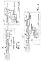
- the transmitter 10 of a modem at one station and receiver 12 of a modem at a second station of an ADSL system is shown.
- the transmitter 10 includes a data source 14, a buffer 16, here a First-In/First Out (FIFO), and a framer 18, arranged as shown.
- the data from the data source 14 is clocked into the FIFO 16 in response to the clock pulses fed thereto from the data source 14.
- the clock pulse rate varies from 0 to about 10 MBtyes per second (MBps).
- the framer 18 produces framed data at the ADSL line rate, which as noted above, is a function of the quality of the line connecting the transmitter 10 and the receiver 12.
- a burst of data is "pulled", or retrieved from, the FIFO 16 in response to a strobe signal supplied by the framer 18. Since the data input rate to the FIFO 16 from data source 14 is asynchronous with respect to the frame rate, byte stuffing or robbing is performed by the framer 18 in order to equalize the rates. This function is performed by a "stuff and rob" section using a level signal from the FIFO 16 to determine if the input rate is lower or higher than the outgoing ADSL line, or frame rate. If the level increases, then the input rate exceeds the ADSL internal rate and an additional byte is passed to the next ADSL frame in a predetermined byte position and signalled in a fast byte or sync byte. That is the signalling that a byte has been stuffed or robbed is passed in the fast byte for the fast data and the synch byte for interleaved data.
- the received data passing through a de-framer 20 which performs a de-stuffing and de-robbing process.
- Synch control information from either the fast or the synch byte, depending on whether the data comes from the fast or interleaved path, is used to determine if the last byte should be blocked from or if additional bytes should be added to the FIFO.
- the output of the de-framer 20 is gated into a FIFO 2.2.
- the data is clocked out of the FIFO 20 using a smooth clock generaLed by a clock pulse generator 24 which can be implemented using a digital phase-locked-loop (DPLL).
- DPLL digital phase-locked-loop
- the transmit path has stuff or rob bytes in the ADSL framing structure to match the ADSL data line rate thereby reducing the data transfer efficiency of the system.
- a system having a source of data.
- the data ie transmitted in response to clock pulses.
- a buffer is provided having a data storage capacity for storing the data transmitted by the source of data.
- the data is stored in response to the clock pulses.
- a framer is provided for retrieving the stored data in response to a strobe signal produced by the framer and fed to the buffer.
- the buffer produces a control signal representative of the fill/empty state of the buffer.
- a clock pulse generator is provided for producing the clock pulses for the data source and the buffer at a rate selected in accordance with the control signal.
- the data stored in the buffer is read from the buffer in response to the strobe signal and such data read from the buffer is supplied to the framer in response to the strobe signal.
- the data provided by the data source and the data written to the buffer are controlled by a common clock signal, which has a rate which is a function of the level of the buffer, thereby ensuring rate matching between the data source rate and the rate data is read from the buffer.
- a common clock signal which has a rate which is a function of the level of the buffer, thereby ensuring rate matching between the data source rate and the rate data is read from the buffer.
- the clock pulse generator includes a digital phase lock loop which locks the frequency of the input data to the rate at which the framer draws data from the FIFO.
- a data transmitter in accordance with one embodiment of the invention, includes a source of data. The data is transmitted in response to clock pulses.
- a buffer having a data storage capacity is provided for storing the data transmitted by the source of data, such data being stored in response to the clock pulses.
- a framer is provided for retrieving the stored data in response to a data strobe signal produced by the framer and fed to the buffer.
- the buffer produces a control signal representative of the fill/empty state of the buffer.
- a fill/empty level signal and superframe strobe signal are fed to the clock pulse generator.
- the superframe strobe signal samples the fill/empty state of the buffer and produces a control signal representative of the sampled level (i.e., fill/empty state) of the buffer.
- a clock pulse generator is provided for producing the clock pulses for the data source and the buffer at a rate selected in accordance with the control signal.
- the data stored in the buffer is read from the buffer in response to the data strobe signal from the framer and such read data from the buffer is supplied to the framer in response to the strobe signal.
- a modem at one station of an ADSL system having a data modem transmitter 30.
- the modem transmitter 30 is fed by a source of data 32.
- the data from the source 32 is received by the modem transmitter 30 in response to clock pulses provided by clock pulse generator 34 in the modem transmitter 30.
- a buffer 36 here a Firet-In/First Out FIFO register in the modem transmitter 30, receives the data from the source 32 in response to the clock pulses provided by the clock pulse generator 34.
- the buffer 32 has a fixed data storage capacity.
- a framer 38 included in the modem transmitter 30 is provided for retrieving the stored data in the FIFO 36 in response to a data strobe signal produced by the framer 38.
- a superframe strobe signal produced by the framer 38 at the start of each superframe of data is fed to the clock pulse synchronizer 34 on line 35.
- a control signal is produced by the buffer 36 on bus 40 representative of the sampled fill/empty state (i.e., level) of the buffer 36.
- the level on bus 40 from the buffer 36 is sampled in response to the superframe strobe signal on line 35.
- the clock pulse generator 34 here a digital phase locked loop, produces the clock pulses for the data source 32 and the buffer 36 at a rate selected in accordance with the control signal on bus 40.
- the phase locked loop locks the input data rate, based upon its own clock, to the ADSL line rate. That is, the phase locked loop locks the frequency of the input data from data source 32 to the rate at which the framer 38 draws data from the FIFO 36.
- the data stored in the buffer 36 is read from the buffer 36 in response to the byte strobe signal on line 37 and such data read from the buffer 36 is supplied to the framer 38 in response to the strobe signal on line 37.
- the data provided by the data source 32 and the data read from the buffer 36 are controlled by a common clock signal provided by the clock pulse generator 34.
- the rate of the clock pulses produced by the clock pulse generator 34 is produced as a function of the level of the buffer, thereby ensuring rate matching between the data source 32 rate and the rate data is read from the buffer 36 by the framer 38. That is, if the level indicates that the buffer 36 is filling too fast, the clock rate is reduced; and, on the other hand, if the level indicates that the buffer 36 is filling too slowly, the clock rate is increased.
- byte stuffing and byte robbing are no longer required thereby allowing a reduced overhead framing mode to be used and increasing the efficiency of the data transfer.
Landscapes
- Engineering & Computer Science (AREA)
- Computer Networks & Wireless Communication (AREA)
- Signal Processing (AREA)
- Synchronisation In Digital Transmission Systems (AREA)
- Time-Division Multiplex Systems (AREA)
Applications Claiming Priority (2)
| Application Number | Priority Date | Filing Date | Title |
|---|---|---|---|
| US09/443,700 US6603831B1 (en) | 1999-11-19 | 1999-11-19 | Synchronous digital data transmitter |
| US443700 | 1999-11-19 |
Publications (3)
| Publication Number | Publication Date |
|---|---|
| EP1102160A2 true EP1102160A2 (de) | 2001-05-23 |
| EP1102160A3 EP1102160A3 (de) | 2005-02-09 |
| EP1102160B1 EP1102160B1 (de) | 2006-08-02 |
Family
ID=23761858
Family Applications (1)
| Application Number | Title | Priority Date | Filing Date |
|---|---|---|---|
| EP00310193A Expired - Lifetime EP1102160B1 (de) | 1999-11-19 | 2000-11-16 | Synchroner Sender von digitalen Daten |
Country Status (3)
| Country | Link |
|---|---|
| US (1) | US6603831B1 (de) |
| EP (1) | EP1102160B1 (de) |
| DE (1) | DE60029723D1 (de) |
Families Citing this family (4)
| Publication number | Priority date | Publication date | Assignee | Title |
|---|---|---|---|---|
| US6731627B1 (en) * | 1998-11-17 | 2004-05-04 | Cisco Technology, Inc. | Virtual loop carrier system |
| US7310390B2 (en) * | 2003-10-30 | 2007-12-18 | Apple Inc. | Decoding coded data streams |
| US20060209684A1 (en) * | 2005-03-18 | 2006-09-21 | Via Technologies, Inc. | Data rate controller, and method of control thereof |
| JP5978792B2 (ja) * | 2012-06-12 | 2016-08-24 | 富士通株式会社 | 伝送装置及び伝送方法 |
Family Cites Families (11)
| Publication number | Priority date | Publication date | Assignee | Title |
|---|---|---|---|---|
| US5204882A (en) * | 1990-12-14 | 1993-04-20 | Bell Communications Research, Inc. | Service clock recovery for variable bit rate services |
| US5473665A (en) * | 1993-03-08 | 1995-12-05 | Adtran | Performance monitoring of DS0 channel via D4 channel bank |
| US5367534A (en) * | 1993-06-16 | 1994-11-22 | Universal Data Systems, Inc. | Synchronous flow control method |
| DE4332761A1 (de) * | 1993-09-25 | 1995-03-30 | Philips Patentverwaltung | Übertragungssystem mit einer Anpassungsschaltung |
| JP3191701B2 (ja) * | 1996-10-29 | 2001-07-23 | 日本電気株式会社 | 伝送フレームフォーマット変換回路 |
| US5903612A (en) * | 1996-11-08 | 1999-05-11 | Alcatel Alsthom Compagnie Generale D'electricite | Method to synchronize data and a transmitter and a receiver realizing said method |
| US6128761A (en) * | 1996-12-13 | 2000-10-03 | Cisco Technology, Inc. | Method and apparatus for G.706 frame alignment and CRC procedure test tool |
| US5778218A (en) * | 1996-12-19 | 1998-07-07 | Advanced Micro Devices, Inc. | Method and apparatus for clock synchronization across an isochronous bus by adjustment of frame clock rates |
| US6157646A (en) * | 1998-01-26 | 2000-12-05 | Adc Telecommunications, Inc. | Circuit and method for service clock recovery |
| US6219730B1 (en) * | 1998-06-20 | 2001-04-17 | Nghi Nho Nguyen | Method and apparatus for producing a combined data stream and recovering therefrom the respective user input stream and at least one additional input signal |
| US6353635B1 (en) * | 1999-02-12 | 2002-03-05 | Microsoft Corporation | Method for simultaneously controlling multiple devices using a single communication channel |
-
1999
- 1999-11-19 US US09/443,700 patent/US6603831B1/en not_active Expired - Lifetime
-
2000
- 2000-11-16 EP EP00310193A patent/EP1102160B1/de not_active Expired - Lifetime
- 2000-11-16 DE DE60029723T patent/DE60029723D1/de not_active Expired - Lifetime
Also Published As
| Publication number | Publication date |
|---|---|
| EP1102160A3 (de) | 2005-02-09 |
| DE60029723D1 (de) | 2006-09-14 |
| EP1102160B1 (de) | 2006-08-02 |
| US6603831B1 (en) | 2003-08-05 |
Similar Documents
| Publication | Publication Date | Title |
|---|---|---|
| USRE39216E1 (en) | Asynchronous processor access to a switch table in a network with isochronous capability | |
| US4569062A (en) | Interface circuit for interfacing between asynchronous data in start/stop format and synchronous data | |
| KR100320391B1 (ko) | 프레임구조를가지는등시성-소스데이타를전송하기위한네트워크 | |
| US5054020A (en) | Apparatus for high speed data communication with asynchronous/synchronous and synchronous/asynchronous data conversion | |
| US5361261A (en) | Frame-based transmission of data | |
| US6937568B1 (en) | Adaptive rate shaping to prevent overflow | |
| US4229815A (en) | Full duplex bit synchronous data rate buffer | |
| EP0565305B1 (de) | Taktsignalübertragung über einen asynchronen Datenkanal | |
| US5903612A (en) | Method to synchronize data and a transmitter and a receiver realizing said method | |
| US6731654B1 (en) | Communication system overhead channel | |
| GB2118400A (en) | Switching digital data signals | |
| US7912078B2 (en) | Credit based flow control in an asymmetric channel environment | |
| JP3427303B2 (ja) | Sdhデータ伝送タイミング | |
| JP2000224199A (ja) | 時分割多重バス同期化信号コンセントレ―タとデ―タ伝送システム及びその方法 | |
| US6993046B1 (en) | Mapping of block-encoded data formats onto a bit/byte synchronous transport medium | |
| US6600745B1 (en) | Cell aligners | |
| US6272138B1 (en) | Method and apparatus for reducing jitter or wander on internetworking between ATM network and PDH network | |
| US6603831B1 (en) | Synchronous digital data transmitter | |
| EP2907280B1 (de) | Verfahren für dynamischen diskontinuierlichen betrieb von einem verteilungspunkt aus | |
| US6813325B1 (en) | System and method to reduce transmit wander in a digital subscriber line | |
| US7372930B2 (en) | Method to synchronize data and a transmitter and a receiver realizing said method | |
| EP0952710A2 (de) | Vorrichtung und Verfahren zur Verbindung von isochronen Systemen über Paketvermittlungsnetze | |
| JP2976732B2 (ja) | 同期光多重化装置 | |
| EP0596650A1 (de) | Vorrichtung und Verfahren zur Anpassung von Kabellängenverzögerungen durch isochrone FIFO' | |
| AU624658B2 (en) | A communication adaptor |
Legal Events
| Date | Code | Title | Description |
|---|---|---|---|
| PUAI | Public reference made under article 153(3) epc to a published international application that has entered the european phase |
Free format text: ORIGINAL CODE: 0009012 |
|
| AK | Designated contracting states |
Kind code of ref document: A2 Designated state(s): AT BE CH CY DE DK ES FI FR GB GR IE IT LI LU MC NL PT SE TR |
|
| AX | Request for extension of the european patent |
Free format text: AL;LT;LV;MK;RO;SI |
|
| PUAL | Search report despatched |
Free format text: ORIGINAL CODE: 0009013 |
|
| AK | Designated contracting states |
Kind code of ref document: A3 Designated state(s): AT BE CH CY DE DK ES FI FR GB GR IE IT LI LU MC NL PT SE TR |
|
| AX | Request for extension of the european patent |
Extension state: AL LT LV MK RO SI |
|
| RIC1 | Information provided on ipc code assigned before grant |
Ipc: 7H 04M 11/06 B Ipc: 7H 04L 12/56 A |
|
| 17P | Request for examination filed |
Effective date: 20050809 |
|
| AKX | Designation fees paid |
Designated state(s): DE FR GB |
|
| GRAP | Despatch of communication of intention to grant a patent |
Free format text: ORIGINAL CODE: EPIDOSNIGR1 |
|
| RIC1 | Information provided on ipc code assigned before grant |
Ipc: H04L 12/56 20060101AFI20060203BHEP Ipc: H04M 11/06 20060101ALI20060203BHEP Ipc: G06F 5/06 20060101ALI20060203BHEP |
|
| GRAS | Grant fee paid |
Free format text: ORIGINAL CODE: EPIDOSNIGR3 |
|
| GRAA | (expected) grant |
Free format text: ORIGINAL CODE: 0009210 |
|
| AK | Designated contracting states |
Kind code of ref document: B1 Designated state(s): DE FR GB |
|
| REG | Reference to a national code |
Ref country code: GB Ref legal event code: FG4D |
|
| REF | Corresponds to: |
Ref document number: 60029723 Country of ref document: DE Date of ref document: 20060914 Kind code of ref document: P |
|
| PG25 | Lapsed in a contracting state [announced via postgrant information from national office to epo] |
Ref country code: DE Free format text: LAPSE BECAUSE OF FAILURE TO SUBMIT A TRANSLATION OF THE DESCRIPTION OR TO PAY THE FEE WITHIN THE PRESCRIBED TIME-LIMIT Effective date: 20061103 |
|
| EN | Fr: translation not filed | ||
| PLBE | No opposition filed within time limit |
Free format text: ORIGINAL CODE: 0009261 |
|
| STAA | Information on the status of an ep patent application or granted ep patent |
Free format text: STATUS: NO OPPOSITION FILED WITHIN TIME LIMIT |
|
| 26N | No opposition filed |
Effective date: 20070503 |
|
| GBPC | Gb: european patent ceased through non-payment of renewal fee |
Effective date: 20061116 |
|
| PG25 | Lapsed in a contracting state [announced via postgrant information from national office to epo] |
Ref country code: GB Free format text: LAPSE BECAUSE OF NON-PAYMENT OF DUE FEES Effective date: 20061116 |
|
| PG25 | Lapsed in a contracting state [announced via postgrant information from national office to epo] |
Ref country code: FR Free format text: LAPSE BECAUSE OF FAILURE TO SUBMIT A TRANSLATION OF THE DESCRIPTION OR TO PAY THE FEE WITHIN THE PRESCRIBED TIME-LIMIT Effective date: 20070511 |
|
| PG25 | Lapsed in a contracting state [announced via postgrant information from national office to epo] |
Ref country code: FR Free format text: LAPSE BECAUSE OF FAILURE TO SUBMIT A TRANSLATION OF THE DESCRIPTION OR TO PAY THE FEE WITHIN THE PRESCRIBED TIME-LIMIT Effective date: 20060802 |