EP1102124A2 - Exposure apparatus and device manufacturing method - Google Patents
Exposure apparatus and device manufacturing method Download PDFInfo
- Publication number
- EP1102124A2 EP1102124A2 EP00310139A EP00310139A EP1102124A2 EP 1102124 A2 EP1102124 A2 EP 1102124A2 EP 00310139 A EP00310139 A EP 00310139A EP 00310139 A EP00310139 A EP 00310139A EP 1102124 A2 EP1102124 A2 EP 1102124A2
- Authority
- EP
- European Patent Office
- Prior art keywords
- organic compound
- gas
- optical element
- exposure apparatus
- decomposition
- Prior art date
- Legal status (The legal status is an assumption and is not a legal conclusion. Google has not performed a legal analysis and makes no representation as to the accuracy of the status listed.)
- Granted
Links
Images


Classifications
-
- G—PHYSICS
- G03—PHOTOGRAPHY; CINEMATOGRAPHY; ANALOGOUS TECHNIQUES USING WAVES OTHER THAN OPTICAL WAVES; ELECTROGRAPHY; HOLOGRAPHY
- G03F—PHOTOMECHANICAL PRODUCTION OF TEXTURED OR PATTERNED SURFACES, e.g. FOR PRINTING, FOR PROCESSING OF SEMICONDUCTOR DEVICES; MATERIALS THEREFOR; ORIGINALS THEREFOR; APPARATUS SPECIALLY ADAPTED THEREFOR
- G03F7/00—Photomechanical, e.g. photolithographic, production of textured or patterned surfaces, e.g. printing surfaces; Materials therefor, e.g. comprising photoresists; Apparatus specially adapted therefor
- G03F7/70—Microphotolithographic exposure; Apparatus therefor
- G03F7/708—Construction of apparatus, e.g. environment aspects, hygiene aspects or materials
- G03F7/70983—Optical system protection, e.g. pellicles or removable covers for protection of mask
-
- G—PHYSICS
- G03—PHOTOGRAPHY; CINEMATOGRAPHY; ANALOGOUS TECHNIQUES USING WAVES OTHER THAN OPTICAL WAVES; ELECTROGRAPHY; HOLOGRAPHY
- G03F—PHOTOMECHANICAL PRODUCTION OF TEXTURED OR PATTERNED SURFACES, e.g. FOR PRINTING, FOR PROCESSING OF SEMICONDUCTOR DEVICES; MATERIALS THEREFOR; ORIGINALS THEREFOR; APPARATUS SPECIALLY ADAPTED THEREFOR
- G03F7/00—Photomechanical, e.g. photolithographic, production of textured or patterned surfaces, e.g. printing surfaces; Materials therefor, e.g. comprising photoresists; Apparatus specially adapted therefor
- G03F7/70—Microphotolithographic exposure; Apparatus therefor
- G03F7/708—Construction of apparatus, e.g. environment aspects, hygiene aspects or materials
- G03F7/70858—Environment aspects, e.g. pressure of beam-path gas, temperature
- G03F7/70883—Environment aspects, e.g. pressure of beam-path gas, temperature of optical system
Definitions
- This invention relates to an exposure apparatus having a light source of a short wavelength such as ultraviolet region and being arranged so that a gas flows around an optical element. Also, it relates to a device manufacturing method using such exposure apparatus.
- substances being present inside the apparatus may be deposited on an optical element to cause light absorption, or matters produced by a photochemical reaction may be deposited on an optical element to deteriorate the optical characteristic thereof. Further, any impurities mixed in a gas along an optical path may function to deteriorate the optical characteristic.
- a filter is used to improve the purity of a gas to be introduced or, alternatively, a gas of a higher purity is supplied, to thereby prevent deposition or to avoid absorption of light by impurities.
- the contamination of the surface of an optical element in an exposure apparatus causes degradation of the optical characteristic thereof.
- the deterioration of the optical characteristic due to such surface deposition of the optical element becomes serious as the wavelength of the light source becomes short. This is for the following reasons.
- filters for removing impurities function to attract impurities at a gas inlet of the apparatus to thereby remove them.
- a filter which uses ion exchange resin, activated charcoal or zeolite may be used.
- a chemical filter having acid matters or alkaline matters attached may be used.
- These filters have own properties, and a single filter does not attract and remove all the impurities.
- an optimum filter may be selected and used in accordance with a substance to be removed. If, therefore, there are different substances to be removed, optimum filters corresponding to these substances should be used in combination. This means that, if there are many varieties of impurities to be removed and they have different properties, a lot of optimum filters corresponding to these properties should be used. Thus, it is necessary to use many filters in combination.
- phthalic acid esters such as dibutyl phthalate (D.B.P.) or dioctyl phthalate (D.O.P.)
- D.B.P. dibutyl phthalate
- D.O.P. dioctyl phthalate
- these substances are organic compounds having a relatively small volatility, since they are used widely as a plasticizer, they will easily become impurities in the atmosphere.
- a photo-washing process for removing matters deposited on an optical element by an optical decomposition reaction based on light irradiation may be done. It has an additional effect of elimination by heating, or an effect of acceleration of decomposition reaction as oxygens are changed to ozones or active oxygens.
- all the substances upon the optical element are not removed. There may be substances remaining on the optical element.
- matters mixed in an ambient gas may react by the irradiation with light, and reaction products may be deposited.
- an exposure apparatus comprising: an optical element; a gas supplying unit for supplying a predetermined gas around said optical element; and an organic compound decomposition mechanism for decomposing and removing an organic compound in the gas.
- the apparatus may further comprise a filter for removing a substance produced by the decomposition of the organic compound.
- the apparatus may further comprise a chamber for accommodating therein a structure to allow the flow of the gas, wherein said organic compound decomposition mechanism may be disposed at at least one of an inlet port of the gas from said gas supplying unit to said chamber and a vicinity of said optical element.
- the organic compound decomposition mechanism may decompose an organic compound by an electric discharging process.
- the organic compound decomposition mechanism may decompose an organic compound on the basis of ionized atoms produced by electric discharging such as plasma discharging and corona discharging.
- the apparatus may further comprise a filter for removing a substance produced by the decomposition of the organic compound based on the discharging process.
- the apparatus may further comprise a filter for removing H 2 O produced by the discharging process.
- the organic compound decomposition mechanism may include a fan for introducing the gas and a flow gauge for monitoring a flow rate of the gas.
- the organic compound decomposition mechanism may adjust said fan on the basis of an output of said flow gauge.
- the organic compound decomposition mechanism may include a catalyst for decomposing ozones.
- the gas may be circulated through said organic compound decomposition mechanism.
- a device manufacturing method comprising the steps of: preparing an exposure apparatus as recited above; and performing an exposure process by use of the exposure apparatus while decomposing an organic compound by use of an organic compound decomposition mechanism of the exposure apparatus.
- the method may further comprise removing a substance produced by the decomposition of the organic compound, by use of a filter.
- an organic compound decomposition mechanism may be provided to decompose and remove an organic compound in a gas on the basis of an electric discharging process. This eliminates the necessity of using many filters in combination. Only a few filters for removing substances produced by the decomposition may be necessary. If the substances produced by the decomposition can be disregarded, these filters may be omitted.
- the organic compound decomposition mechanism may be provided in the vicinity of an optical element.
- Figure 1 is a schematic view of a main portion of an exposure apparatus with optical elements, according to an embodiment of the present invention.
- Figure 2 is a schematic view of an organic compound and impurity removing mechanism in the apparatus of Figure 1.
- Figure 3 is a schematic view of a main portion of an exposure apparatus, with a purged gas circulation mechanism, according to another embodiment of the present invention.
- Figure 4 is a flow chart of device manufacturing processes in which an exposure apparatus according to the present invention can be used.
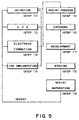
- Figure 5 is a flow chart for explaining details of a wafer process in the procedure shown in Figure 4.
- each organic compound decomposition mechanism has an electrode for electric discharging. Through the electric discharging by the electrode, organic compounds can be decomposed, such that organic compounds contained in the gas flowing to the optical element can be removed.
- Figure 1 is a schematic view of the exposure apparatus of this embodiment, and it shows an optical system in a space in which optical elements are gas-purged.
- Denoted in Figure 1 at 1 are optical elements (lenses), and denoted at 2 are lens supports for supporting the optical elements (lenses).
- Denoted at 20 is a chamber for accommodating the structure therein while allowing the flow of a gas, and denoted at 3 are gas inlet ports for introducing gases into the chamber.
- Denoted at 4 are gas supplying units for supplying gases through the inlet ports 3, and denoted at 5 are gas outlet ports for discharging gases from the chamber.
- Denoted at 6 are exhaust units for discharging gases through the outlet ports 5.
- Denoted at 7 are organic compound decomposition mechanisms which are provided just before the gas inlet ports 3, respectively.
- Denoted at 8 are organic compound decomposition mechanisms which are disposed adjacent the optical elements 1.
- each organic compound decomposition mechanism 7 is provided just before the gas inlet port 3.
- organic compounds which may contain degased components from the members of the gas supplying unit 4 can be decomposed and removed.
- the organic compound decomposition mechanisms 8 are provided in the vicinity of the optical elements 1.
- Each organic compound decomposition mechanism 8 includes a gas introducing port at the lens support or at an inside wall of the structure, from which a gas which contains organic compounds as degased components from the members is introduced, and the organic compound decomposition process is performed.
- Each organic compound decomposition mechanism 8 has a gas discharging port, facing to the optical element (lens). From these gas discharging ports, gases with organic compounds removed are discharged toward the lenses, such that clean gases are supplied to the lens surfaces.
- FIG. 2 is a schematic view of one organic compound decomposition mechanism. It includes an electric discharging unit 9 which comprises a pair or more of a discharging electrode and an opposed electrode, necessary for corona discharge or plasma discharge for decomposition of organic compounds. Through the electric discharge such as corona discharge or plasma discharge in the discharging unit 9, ionized atoms are produced. At a portion downstream of the discharging unit 9, there is a filter unit 10 which is provided, as desired, to remove substances to be produced as a result of the decomposition of organic compounds. Due to the decomposition by electric discharge, an organic compound is changed to have a simpler structure. Also, the kinds of organic compounds are reduced. Therefore, the filter unit 10 needs only a few filters to be used.
- the filter unit 10 may be omitted.
- H 2 O itself is a matter that may cause deterioration of the optical performance but also there is a possibility that it reacts with a degased component from a resist, for example, to produce ammonia or ammonium ion. These substances may be adhered to and deposited on an optical element to cause deterioration of the optical characteristic thereof. Therefore, it is necessary to move H 2 O sufficiently. In this respect, use of a filter for removing H 2 O is particularly preferable.
- the filter unit 10 may be provided with an ozone decomposing catalyst for decomposing ozones.
- an ozone decomposing catalyst for decomposing ozones.
- a catalyst containing manganese dioxide is widely known.
- ozones can be reduced to oxygens by use of activated charcoal.
- an ozone concentration gauge may be provided so that the discharging voltage may be adjusted while monitoring the ozone concentration. With this arrangement, adverse influence of ozones to surfaces of components of the exposure apparatus can be prevented. Since no discharge occurs with a too low voltage, in the presence of oxygens the discharging voltage may preferably be set in a range of 5 - 10 kV.
- the electrode of the discharging unit 9 may have a honeycomb structure by which the contact area with the gas as well as the electric discharging efficiency can be increased. Further, the space to be occupied can be made smaller. Similar advantageous results are attainable where a spiral structure or a layered (laminated) structure is used. As regards an opposed electrode to such discharging electrode, it should have an electric conductivity to assure the discharging. Where a material having a catalyst function such as platinum or palladium, for example, is used, the effect thereof can be improved.
- the gas may be circulated inside the exposure apparatus or the gas discharged outwardly through the outlet port of the exposure apparatus may be introduced into an inlet port of the apparatus for the circulation, by which the apparatus can be operated stably without a large consumption of gases.
- Circulating a purge gas is very effective in respect to the cost, particularly when a helium gas which is expensive as compared with a clean dry air or a nitrogen gas is used as the purge gas.
- FIG. 3 is a schematic view of an optical system in a space in which optical elements of an exposure apparatus are purged with a gas which is circulated in the structure.
- Gases which are discharged through gas discharging ports 5 are flown through a gas circulation unit 13 and introduced into the structure from gas inlet ports 3.
- Organic compound decomposition mechanisms 7 disposed just before the gas inlet ports 3 decompose and remove organic compounds.
- There is an electromagnetic valve 14 which functions to discharge the circulated gas outwardly through a discharging unit 6 and also to supply a fresh gas from a gas supplying unit 4.
- the circulation gas exchange is made in this manner. Such circulation gas exchange may be done at regular periods in which the removal of impurities is made sufficiently.
- a sensor 16 may be provided to monitor the concentration of organic compounds such that, when the concentration becomes higher than a predetermined level, the electromagnetic valve 14 may be actuated through a controller 15 to execute the gas exchange.
- this embodiment is not limited to use of an electromagnetic valve.
- a variable valve by which the flow rate can be adjusted may be used. In such case, the adjustment of the flow rate of the variable valve may be controlled in accordance with a signal from the sensor 16, concerning the concentration of organic compounds.
- the placement of the organic compound decomposition mechanism is not limited to at the inlet port 3 of the chamber or in the vicinity of the optical element 1, as illustrated.
- the mechanism may be provided in a portion of the path of the gas circulation unit 13.
- Organic compound decomposition mechanisms having discharging electrodes were mounted adjacent every optical elements such as lenses and mirrors of a KrF exposure apparatus, using a clean dry air as a purge gas.
- Each organic compound decomposition mechanism was provided with an ozone decomposition catalyst, mainly containing manganese dioxide, disposed after the discharging unit 9.
- ozone decomposition catalyst mainly containing manganese dioxide
- every optical element is equipped with an organic compound decomposition mechanism disposed adjacent it.
- organic compound decomposition mechanism may be provided only in portions where the influence of degradation of the optical performance is large.
- the ozone decomposition catalyst used one having manganese dioxide as a major component, a catalyst without manganese dioxide may be used as long as it has a function of ozone decomposition.
- Example 3 the removal of organic compounds was carried out in a similar manner as Example 3 above, except that a helium gas was used as a purge gas in an ArF exposure apparatus. Also in this example, production of substances upon optical elements, causing absorption, was prevented, and deterioration of the optical characteristic was avoided.
- organic compound decomposition mechanisms having discharging electrodes were mounted adjacent to optical elements such as lenses and mirrors.
- the decomposition and removal of organic compounds were carried out in a similar manner as Example 3 above, by use of a nitrogen gas or a helium gas as a purge gas. Also in this example, production of substances upon optical elements, causing absorption, was prevented, and deterioration of the optical characteristic was avoided.
- Figure 4 is a flow chart of procedure for manufacture of microdevices such as semiconductor chips (e.g. ICs or LSIs), liquid crystal panels, CCDs, thin film magnetic heads or micro-machines, for example.
- semiconductor chips e.g. ICs or LSIs
- liquid crystal panels e.g. CCDs
- thin film magnetic heads e.g. MEMS-machines
- Step 1 is a design process for designing a circuit of a semiconductor device.
- Step 2 is a process for making a mask on the basis of the circuit pattern design.
- Step 3 is a process for preparing a wafer by using a material such as silicon.
- Step 4 is a wafer process (called a pre-process) wherein, by using the so prepared mask and wafer, circuits are practically formed on the wafer through lithography.
- Step 5 subsequent to this is an assembling step (called a post-process) wherein the wafer having been processed by step 4 is formed into semiconductor chips.
- This step includes an assembling (dicing and bonding) process and a packaging (chip sealing) process.
- Step 6 is an inspection step wherein operation check, durability check and so on for the semiconductor devices provided by step 5, are carried out. With these processes, semiconductor devices are completed and they are shipped (step 7).
- Figure 5 is a flow chart showing details of the wafer process.
- Step 11 is an oxidation process for oxidizing the surface of a wafer.
- Step 12 is a CVD process for forming an insulating film on the wafer surface.
- Step 13 is an electrode forming process for forming electrodes upon-the wafer by vapor deposition.
- Step 14 is an ion implanting process for implanting ions to the wafer.
- Step 15 is a resist process for applying a resist (photosensitive material) to the wafer.
- Step 16 is an exposure process for printing, by exposure, the circuit pattern of the mask on the wafer through the exposure apparatus described above.
- Step 17 is a developing process for developing the exposed wafer.
- Step 18 is an etching process for removing portions other than the developed resist image.
- Step 19 is a resist separation process for separating the resist material remaining on the wafer after being subjected to the etching process. By repeating these processes, circuit patterns are superposedly formed on the wafer.
- organic compound removing means for removing organic compounds in a gas on the basis of electric discharge effectively avoids the necessity of using many filters in combination, and it prevents adhesion of organic compounds on an optical element.
- the organic substance decomposition means may be provided adjacent to an optical element, by which a degased component from an inside members can also be removed. This effectively assures that no organic compound is present in a gas flowing along the surface of the optical element. As a result of it, deterioration of the optical performance of the optical element can be prevented effectively.
- a supplied gas may be circulated and purified through organic compound decomposition means. This provides an exposure apparatus which does not consume a large quantity of gas and thus which is very effective in respect to the cost. Further, in accordance with a device manufacturing method using such exposure apparatus, a high precision exposure process can be performed without degradation, and very precise devices can be produced thereby.
Landscapes
- Health & Medical Sciences (AREA)
- Engineering & Computer Science (AREA)
- Environmental & Geological Engineering (AREA)
- Epidemiology (AREA)
- Public Health (AREA)
- Physics & Mathematics (AREA)
- General Physics & Mathematics (AREA)
- Life Sciences & Earth Sciences (AREA)
- Atmospheric Sciences (AREA)
- Toxicology (AREA)
- Exposure Of Semiconductors, Excluding Electron Or Ion Beam Exposure (AREA)
- Exposure And Positioning Against Photoresist Photosensitive Materials (AREA)
Abstract
Description
Claims (15)
- An exposure apparatus, comprising:an optical element;a gas supplying unit for supplying a predetermined gas around said optical element; andan organic compound decomposition mechanism for decomposing an organic compound in the gas.
- An apparatus according to Claim 1, further comprising a filter for removing a substance produced by the decomposition of the organic compound.
- An apparatus according to Claim 1, further comprising a chamber for accommodating therein a structure to allow the flow of the gas, wherein said organic compound decomposition mechanism is disposed at at least one of an inlet port of the gas from said gas supplying unit to said chamber and a vicinity of said optical element.
- An apparatus according to any one of Claims 1 - 3, wherein said organic compound decomposition mechanism decomposes an organic compound by an electric discharging process.
- An apparatus according to Claim 4, wherein said organic compound decomposition mechanism decomposes an organic compound on the basis of ionized atoms produced by electric discharging such as plasma discharging and corona discharging.
- An apparatus according to Claim 4 or 5, further comprising a filter for removing a substance produced by the decomposition of the organic compound based on the discharging process.
- An apparatus according to any one of Claims 4 - 6, further comprising a filter for removing H2O produced by the discharging process.
- An apparatus according to any one of Claims 1 - 7, wherein said organic compound decomposition mechanism includes a fan for introducing the gas and a flow gauge for monitoring a flow rate of the gas.
- An apparatus according to Claim 8, wherein said organic compound decomposition mechanism adjusts said fan on the basis of an output of said flow gauge.
- An apparatus according to any one of Claims 1 - 9, wherein said organic compound decomposition mechanism includes a catalyst for decomposing ozones.
- An apparatus according to any one of Claims 1 - 10, wherein the gas is circulated through said organic compound decomposition mechanism.
- A device manufacturing method, comprising the steps of:preparing an exposure apparatus as recited in any one of claims 1 - 11; andperforming an exposure process to apply a pattern to a substrate by use of the exposure apparatus while decomposing an organic compound by use of an organic compound decomposition mechanism of the exposure apparatus; andmanufacturing a device from the patterned substrate.
- A method according to claim 12, further comprising removing a substance produced by the decomposition of the organic compound, by use of a filter.
- An exposure apparatus, comprising:an optical element;a housing for containing a gas surrounding the optical element;an organic compound decomposing means for decomposing an organic compound in the gas, having an inlet for gas and an outlet for treated gas; and means to direct the treated gas from the outlet to the vicinity of the optical element.
- An exposure apparatus according to claim 14, wherein the treated gas is directed to flow across a surface of the optical element.
Applications Claiming Priority (2)
| Application Number | Priority Date | Filing Date | Title |
|---|---|---|---|
| JP32578599A JP2001144003A (en) | 1999-11-16 | 1999-11-16 | Exposure apparatus and device manufacturing method |
| JP32578599 | 1999-11-16 |
Publications (3)
| Publication Number | Publication Date |
|---|---|
| EP1102124A2 true EP1102124A2 (en) | 2001-05-23 |
| EP1102124A3 EP1102124A3 (en) | 2002-04-17 |
| EP1102124B1 EP1102124B1 (en) | 2007-05-02 |
Family
ID=18180589
Family Applications (1)
| Application Number | Title | Priority Date | Filing Date |
|---|---|---|---|
| EP00310139A Expired - Lifetime EP1102124B1 (en) | 1999-11-16 | 2000-11-15 | Exposure apparatus and device manufacturing method |
Country Status (4)
| Country | Link |
|---|---|
| US (1) | US6819396B1 (en) |
| EP (1) | EP1102124B1 (en) |
| JP (1) | JP2001144003A (en) |
| DE (1) | DE60034645D1 (en) |
Families Citing this family (3)
| Publication number | Priority date | Publication date | Assignee | Title |
|---|---|---|---|---|
| US7476491B2 (en) * | 2004-09-15 | 2009-01-13 | Asml Netherlands B.V. | Lithographic apparatus, gas supply system, method for purging, and device manufacturing method and device manufactured thereby |
| KR100660892B1 (en) * | 2005-11-21 | 2006-12-26 | 삼성전자주식회사 | Circuit and Method for Sampling Valid Commands with Extended Valid Address Window for High Speed Operation in Double Pumped Address Schemes |
| JP6818037B2 (en) * | 2016-09-30 | 2021-01-20 | 富士フイルム株式会社 | Semiconductor chip manufacturing method, kit |
Family Cites Families (36)
| Publication number | Priority date | Publication date | Assignee | Title |
|---|---|---|---|---|
| JPS57122924A (en) * | 1981-01-21 | 1982-07-31 | Tokyo Roki Kk | Filter for decomposing ozone |
| JPH01265513A (en) * | 1988-04-15 | 1989-10-23 | Nec Corp | Reduction projection aligner |
| US5531857A (en) | 1988-07-08 | 1996-07-02 | Cauldron Limited Partnership | Removal of surface contaminants by irradiation from a high energy source |
| US5024968A (en) | 1988-07-08 | 1991-06-18 | Engelsberg Audrey C | Removal of surface contaminants by irradiation from a high-energy source |
| US6048588A (en) | 1988-07-08 | 2000-04-11 | Cauldron Limited Partnership | Method for enhancing chemisorption of material |
| US5821175A (en) | 1988-07-08 | 1998-10-13 | Cauldron Limited Partnership | Removal of surface contaminants by irradiation using various methods to achieve desired inert gas flow over treated surface |
| US5643472A (en) | 1988-07-08 | 1997-07-01 | Cauldron Limited Partnership | Selective removal of material by irradiation |
| US5099557A (en) | 1988-07-08 | 1992-03-31 | Engelsberg Audrey C | Removal of surface contaminants by irradiation from a high-energy source |
| US5221520A (en) * | 1991-09-27 | 1993-06-22 | North Carolina Center For Scientific Research, Inc. | Apparatus for treating indoor air |
| JP3306912B2 (en) | 1992-07-23 | 2002-07-24 | 株式会社ニコン | UV irradiation apparatus, UV irradiation method, and exposure method |
| JP3265666B2 (en) | 1992-07-01 | 2002-03-11 | 株式会社ニコン | Exposure equipment |
| US5430303A (en) * | 1992-07-01 | 1995-07-04 | Nikon Corporation | Exposure apparatus |
| JPH06323571A (en) * | 1993-05-10 | 1994-11-25 | Daikin Ind Ltd | Air conditioner |
| JP3448670B2 (en) | 1993-09-02 | 2003-09-22 | 株式会社ニコン | Exposure apparatus and element manufacturing method |
| BE1007851A3 (en) | 1993-12-03 | 1995-11-07 | Asml Lithography B V | EXPOSURE UNIT WITH ANTI-POLLUTION DEVICE AND A PHOTOLITHOGRAPHIC DEVICE EQUIPPED WITH SUCH AN EXPOSURE UNIT. |
| BE1007907A3 (en) | 1993-12-24 | 1995-11-14 | Asm Lithography Bv | LENS SYSTEM WITH HOLDER MADE IN gasfilled lens elements and photolithographic DEVICE WITH SUCH A SYSTEM. |
| US5685895A (en) | 1994-08-10 | 1997-11-11 | Nikon Corporation | Air cleaning apparatus used for an exposure apparatus |
| JPH08306599A (en) | 1995-04-27 | 1996-11-22 | Nikon Corp | Air purification device and exposure device |
| JP3433844B2 (en) | 1994-08-10 | 2003-08-04 | 株式会社ニコン | Filter device for exposure apparatus and projection exposure apparatus |
| TW284907B (en) | 1995-06-07 | 1996-09-01 | Cauldron Lp | Removal of material by polarized irradiation and back side application for radiation |
| US5667564A (en) | 1996-08-14 | 1997-09-16 | Wein Products, Inc. | Portable personal corona discharge device for destruction of airborne microbes and chemical toxins |
| JPH10112429A (en) | 1996-10-07 | 1998-04-28 | Nippon Telegr & Teleph Corp <Ntt> | Light exposure system |
| US6194821B1 (en) * | 1997-02-12 | 2001-02-27 | Quark Systems Co., Ltd. | Decomposition apparatus of organic compound, decomposition method thereof, excimer UV lamp and excimer emission apparatus |
| JPH10242029A (en) * | 1997-02-27 | 1998-09-11 | Canon Inc | Exposure equipment |
| JP3004938B2 (en) * | 1997-03-07 | 2000-01-31 | 株式会社オーデン | Electric dust collector and method of manufacturing the same |
| JPH10270333A (en) * | 1997-03-27 | 1998-10-09 | Nikon Corp | Exposure equipment |
| JPH10289854A (en) | 1997-04-15 | 1998-10-27 | Canon Inc | Exposure equipment |
| JP3635860B2 (en) | 1997-05-14 | 2005-04-06 | 株式会社ニコン | Optical device |
| TW420829B (en) * | 1997-05-22 | 2001-02-01 | Tokyo Electron Ltd | Treatment device and method, impurity removing apparatus |
| WO1998057213A1 (en) * | 1997-06-10 | 1998-12-17 | Nikon Corporation | Optical device, method of cleaning the same, projection aligner, and method of producing the same |
| JPH1167618A (en) | 1997-08-15 | 1999-03-09 | Nippon Telegr & Teleph Corp <Ntt> | Accommodation equipment |
| JP3445120B2 (en) | 1997-09-30 | 2003-09-08 | キヤノン株式会社 | Exposure apparatus and device manufacturing method |
| JPH11111593A (en) | 1997-10-01 | 1999-04-23 | Canon Inc | Environmental control device |
| US6036738A (en) * | 1997-12-31 | 2000-03-14 | Shanbrom Technologies Llc | Disinfecting gas filters |
| JPH11204411A (en) * | 1998-01-19 | 1999-07-30 | Nikon Corp | Coating development exposure equipment |
| EP0957402B1 (en) * | 1998-05-15 | 2006-09-20 | ASML Netherlands B.V. | Lithographic device |
-
1999
- 1999-11-16 JP JP32578599A patent/JP2001144003A/en active Pending
-
2000
- 2000-11-15 EP EP00310139A patent/EP1102124B1/en not_active Expired - Lifetime
- 2000-11-15 DE DE60034645T patent/DE60034645D1/en not_active Expired - Lifetime
- 2000-11-16 US US09/712,979 patent/US6819396B1/en not_active Expired - Fee Related
Also Published As
| Publication number | Publication date |
|---|---|
| DE60034645D1 (en) | 2007-06-14 |
| US6819396B1 (en) | 2004-11-16 |
| JP2001144003A (en) | 2001-05-25 |
| EP1102124A3 (en) | 2002-04-17 |
| EP1102124B1 (en) | 2007-05-02 |
Similar Documents
| Publication | Publication Date | Title |
|---|---|---|
| US6252648B1 (en) | Exposure apparatus and method of cleaning optical element of the same | |
| US20020018190A1 (en) | Exposure apparatus and device manufacturing method | |
| US6924877B2 (en) | Chemical filter arrangement for a semiconductor manufacturing apparatus | |
| JPH11145053A (en) | Exposure apparatus and device manufacturing method | |
| US6356338B2 (en) | Semiconductor production system with an in-line subsystem | |
| EP1102124B1 (en) | Exposure apparatus and device manufacturing method | |
| JP2000306807A (en) | Exposure apparatus, exposure method, and semiconductor device manufacturing method | |
| JP2000208407A (en) | Exposure equipment | |
| US6914667B2 (en) | Exposure apparatus and purging method for the same | |
| US6449332B1 (en) | Exposure apparatus, and device manufacturing method | |
| US6762822B2 (en) | Exposure apparatus and manufacturing method using the same | |
| JP2006245401A (en) | Exposure apparatus and device manufacturing method | |
| US7251014B2 (en) | Exposing method, exposing apparatus and device manufacturing method utilizing them | |
| JPH11111593A (en) | Environmental control device | |
| JP2003234281A (en) | Exposure apparatus and device manufacturing method | |
| US6418187B1 (en) | X-ray mask structure, and X-ray exposure method and apparatus using the same | |
| JP2001143987A (en) | Exposure equipment | |
| JP4438072B2 (en) | Method for cleaning lens of exposure apparatus | |
| JP4724537B2 (en) | Exposure equipment | |
| WO2002065183A1 (en) | Lens-barrel, exposure device, and method of manufacturing device | |
| JP4878082B2 (en) | Exposure apparatus and device manufacturing method | |
| JP2001028331A (en) | Optical apparatus, exposure apparatus using the same, and gas inflow method | |
| JP2002134389A (en) | Exposure equipment | |
| JP2005129630A (en) | Purge nozzle, exposure apparatus using the same, and device manufacturing method | |
| JPH11195576A (en) | Exposure equipment |
Legal Events
| Date | Code | Title | Description |
|---|---|---|---|
| PUAI | Public reference made under article 153(3) epc to a published international application that has entered the european phase |
Free format text: ORIGINAL CODE: 0009012 |
|
| AK | Designated contracting states |
Kind code of ref document: A2 Designated state(s): AT BE CH CY DE DK ES FI FR GB GR IE IT LI LU MC NL PT SE TR Kind code of ref document: A2 Designated state(s): DE GB NL |
|
| AX | Request for extension of the european patent |
Free format text: AL;LT;LV;MK;RO;SI |
|
| PUAL | Search report despatched |
Free format text: ORIGINAL CODE: 0009013 |
|
| AK | Designated contracting states |
Kind code of ref document: A3 Designated state(s): AT BE CH CY DE DK ES FI FR GB GR IE IT LI LU MC NL PT SE TR |
|
| AX | Request for extension of the european patent |
Free format text: AL;LT;LV;MK;RO;SI |
|
| 17P | Request for examination filed |
Effective date: 20020925 |
|
| AKX | Designation fees paid |
Free format text: DE GB NL |
|
| 17Q | First examination report despatched |
Effective date: 20050502 |
|
| GRAP | Despatch of communication of intention to grant a patent |
Free format text: ORIGINAL CODE: EPIDOSNIGR1 |
|
| RIN1 | Information on inventor provided before grant (corrected) |
Inventor name: TSUKAMOTO, MASAMI,C/O CANON KABUSHIKI KAISHA Inventor name: TANABE, MASAYUKI,C/O CANON KABUSHIKI KAISHA Inventor name: FUKUDA, YASUAKI,C/O CANON KABUSHIKI KAISHA |
|
| GRAS | Grant fee paid |
Free format text: ORIGINAL CODE: EPIDOSNIGR3 |
|
| GRAA | (expected) grant |
Free format text: ORIGINAL CODE: 0009210 |
|
| AK | Designated contracting states |
Kind code of ref document: B1 Designated state(s): DE GB NL |
|
| REG | Reference to a national code |
Ref country code: GB Ref legal event code: FG4D |
|
| REF | Corresponds to: |
Ref document number: 60034645 Country of ref document: DE Date of ref document: 20070614 Kind code of ref document: P |
|
| NLV1 | Nl: lapsed or annulled due to failure to fulfill the requirements of art. 29p and 29m of the patents act | ||
| PG25 | Lapsed in a contracting state [announced via postgrant information from national office to epo] |
Ref country code: NL Free format text: LAPSE BECAUSE OF FAILURE TO SUBMIT A TRANSLATION OF THE DESCRIPTION OR TO PAY THE FEE WITHIN THE PRESCRIBED TIME-LIMIT Effective date: 20070502 |
|
| PLBE | No opposition filed within time limit |
Free format text: ORIGINAL CODE: 0009261 |
|
| STAA | Information on the status of an ep patent application or granted ep patent |
Free format text: STATUS: NO OPPOSITION FILED WITHIN TIME LIMIT |
|
| 26N | No opposition filed |
Effective date: 20080205 |
|
| PG25 | Lapsed in a contracting state [announced via postgrant information from national office to epo] |
Ref country code: DE Free format text: LAPSE BECAUSE OF FAILURE TO SUBMIT A TRANSLATION OF THE DESCRIPTION OR TO PAY THE FEE WITHIN THE PRESCRIBED TIME-LIMIT Effective date: 20070803 |
|
| PGFP | Annual fee paid to national office [announced via postgrant information from national office to epo] |
Ref country code: GB Payment date: 20081124 Year of fee payment: 9 |
|
| GBPC | Gb: european patent ceased through non-payment of renewal fee |
Effective date: 20091115 |
|
| PG25 | Lapsed in a contracting state [announced via postgrant information from national office to epo] |
Ref country code: GB Free format text: LAPSE BECAUSE OF NON-PAYMENT OF DUE FEES Effective date: 20091115 |