EP1100122A2 - Die used for resin-sealing and molding an electronic component - Google Patents
Die used for resin-sealing and molding an electronic component Download PDFInfo
- Publication number
- EP1100122A2 EP1100122A2 EP00309855A EP00309855A EP1100122A2 EP 1100122 A2 EP1100122 A2 EP 1100122A2 EP 00309855 A EP00309855 A EP 00309855A EP 00309855 A EP00309855 A EP 00309855A EP 1100122 A2 EP1100122 A2 EP 1100122A2
- Authority
- EP
- European Patent Office
- Prior art keywords
- die
- resin
- coating layer
- electronic component
- pot
- Prior art date
- Legal status (The legal status is an assumption and is not a legal conclusion. Google has not performed a legal analysis and makes no representation as to the accuracy of the status listed.)
- Withdrawn
Links
Images

Classifications
-
- H—ELECTRICITY
- H10—SEMICONDUCTOR DEVICES; ELECTRIC SOLID-STATE DEVICES NOT OTHERWISE PROVIDED FOR
- H10W—GENERIC PACKAGES, INTERCONNECTIONS, CONNECTORS OR OTHER CONSTRUCTIONAL DETAILS OF DEVICES COVERED BY CLASS H10
- H10W76/00—Containers; Fillings or auxiliary members therefor; Seals
- H10W76/40—Fillings or auxiliary members in containers, e.g. centering rings
- H10W76/42—Fillings
-
- H—ELECTRICITY
- H10—SEMICONDUCTOR DEVICES; ELECTRIC SOLID-STATE DEVICES NOT OTHERWISE PROVIDED FOR
- H10W—GENERIC PACKAGES, INTERCONNECTIONS, CONNECTORS OR OTHER CONSTRUCTIONAL DETAILS OF DEVICES COVERED BY CLASS H10
- H10W74/00—Encapsulations, e.g. protective coatings
- H10W74/01—Manufacture or treatment
- H10W74/016—Manufacture or treatment using moulds
Definitions
- the present invention relates to an improvement of a die used for sealing an electronic component such as an integrated circuit (IC) with resin to mold the same.
- IC integrated circuit
- top and bottom dies a resin-sealing and molding die formed of a top, fixed die and a bottom, movable die
- the top and bottom dies are previously heated by heating means to have a temperature at which resin is molded, and the top and bottom dies are opened. Then, a lead frame with an electronic component mounted thereto is fed and set in the bottom die's parting-line (P.L) plane (a die plane) at a predetermined position and a resin material is fed into a pot in the bottom die. Then, the bottom, movable die is moved upward and the both dies are closed, when the electronic component and the lead frame therearound are fit into upper and lower cavities respectively provided in the top and bottom dies on their respective one sides and facing each other and the resin material in the pot is heated and gradually melted.
- P.L parting-line
- the heated and melted resin material in the pot is introduced through a resin channel and thus injected into and fills the both of the upper and lower cavities and the electronic component and lead frame therearound in the upper and lower cavities are thus shielded with the resin and thus molded internal to a resin shielded body to correspond to the shape of the upper and lower cavities.
- the both dies are opened and an ejector pin provided in the both dies is employed to release the resin-molded body and lead frame in the upper and lower cavities and the resin cured in the resin channel.
- the above, conventional die typically has a surface plated with hard chromium (HCr).
- HCr hard chromium
- the upper and lower cavities both have a surface highly adhesive to a resin molded body.
- an ejector pin is not sufficient to eject and thus release the resin molded body from the cavities.
- a resin molded body (a product) readily chips if an ejector pin is used to eject and thus release the resin molded body from the upper and lower cavities.
- melted resin material readily enters the P. L plane of the dies and resin flash (the resin cured) remains and thus readily adheres.
- the adhering resin flash affects product size and the like and also enters the resin molded body to prevent uniform production of products.
- the die cavity would be tightly sealed and cannot exhaust its internal air through the air vent.
- the air in the die cavity is introduced into the resin molded body and the resin molded body would have a portion which is not filled with the resin.
- a resin material is compounded with an increased amount of a mold release agent, although the mold release agent would degrade the adhesion between a surface of a lead frame made of metal and a resin molded body (the resin cured).
- the die must have its surface frequently cleaned to remove resin flash remaining and thus adhering to the die surface. This would make the die surface cleaning difficult and time-consuming, resulting in an increased die molding cycle time.
- the product is produced at a low level of productivity.
- the present invention contemplates a die used for sealing an electronic component with resin to mold the electronic component, capable of improving the releaseability of a resin molded body with respect to the die to release the body from the die more efficiently.
- the present invention also contemplates a die used for sealing an electronic component with resin to mold the electronic component, capable of providing a high quality product that is highly reliable.
- the present invention also contemplates a die used for sealing an electronic component with resin to mold the electronic component, capable of enhancing the productivity for the product.
- the present invention provides the die used for sealing the electronic component with resin to mold the electronic component, having a coating layer of nickel-tungsten alloy on at least a surface thereof contacting a melted resin material when the resin is molded.
- the present invention in one embodiment provides the die used for sealing the electronic component with resin to mold the electronic component, wherein the coating layer is a plating layer formed of a nickel-tungsten alloy containing at least 20% by weight of tungsten.
- NiW nickel-tungsten alloy
- the resin molded body can be efficiently ejected and released from the die cavities and the die can also be efficiently prevented from having resin flash (cured resin) adhering to its P. L plane or the like.
- the surface provided with the NiW layer is greater in hardness than a surface processed with HCr. Thus, abrading and damaging the die can be minimized to enhance the durability of the die.
- the present invention can effectively provide a die used for sealing an electronic component with resin to mold the electronic component that is capable of providing a high-quality product that is highly reliable at a high level of productivity.
- the present invention in one embodiment provides the coating layer (A) having a tungsten content of 20% by weight for the following reasons:
- a basic bathing of a nickel-tungsten alloy plating has a tungsten content below 20% by weight, e.g., 10% by weight, it would be a bathing which has a high temperature of 70 to 95°C and is ammonium-alkaline with pH 8 to 9.
- This high-temperature bathing contains ammonium significantly volatile and it can thus hardly be controlled. The ammonium also smells bad and thus degrades the working environment of interest.
- coating layer (A) has a tungsten content of approximately 10% by weight then electrolysis rapidly increases the layer's electrostatic stress also decreases the layer's flexibility. This results in a crack in a surface of the coating layer.
- the nickel-tungsten alloy plating as it is has a hardness of approximately Hv. 600
- the plating heated and thus cured can be as hard as Hv. 1350.
- a nickel-tungsten alloy plating with a tungsten content of approximately 10% by weight is heated to be cured, it does not cure in separation and can only have a hardness of approximately Hv. 600, the hardness of the exact plating which is no further processed.
- a nickel-tungsten alloy plating containing no less than 20% by weight of tungsten is advantageous in that it is not corroded by concentrated hydrochloric acid, sulfuric acid, hydrofluoric acid, or nitric acid.
- tungsten is not separated from a solution with its ions existing independently and an induced eutectoid reaction occurs.
- tungsten is contained with an upper limit of approximately 60% by weight.
- coating layer (A) provided on the surface that a melted resin material contacts in sealing and molding preferably has a tungsten content of no more than 60% by weight.
- coating layer (A) is preferably lum to 20 ⁇ m in thickness, since coating layer (A) exceeding 20 ⁇ m in thickness has a spherical crystal and can thus not have a reliable surface and coating layer (A) less than 1 ⁇ m in thickness is too thin to effectively plate a surface.
- the present invention can be applied to a resin-sealing and molding die for example including a fixed die, a movable die arranged opposite to the fixed die, upper and lower cavities provided in the fixed die and the movable die in their respective die planes to face each other along a parting-line plane of the fixed die and the movable die, for molding the resin, a concavity receiving and setting a support having the electronic component mounted thereto, a pot arranged at one of the fixed die and the movable die for supplying the resin material, a plunger fit internal to the pot for applying pressure to the resin, and a resin channel to allow the pot and the upper cavity to communicate with each other for transporting the melted resin material, wherein the coating layer is provided on an internal surface of the upper and lower cavities, an internal surface of the resin channel, an internal surface of the concavity, an internal surface of the pot, the parting-line plane of each of the fixed die and the movable die, and an external surface of the plunger.
- the die further includes an ejector pin ejecting and releasing from the upper and lower cavities a resin-molded body molded in the upper and lower cavities and an ejector pin fitting hole fitting the ejector pin therein, preferably the ejector pin has an external surface provided with the coating layer of nickel-tungsten alloy and/or the ejector pin fitting hole has an internal surface provided with the coating layer of nickel-tungsten alloy.
- the present invention in one embodiment provides a die formed of a fixed, top die 1, a movable, bottom die 2 arranged opposite to top die 1, upper and lower cavities 3 and 4 provided in dies 1 and 2 in their respective die planes to face each other along the P.
- L plane of dies 1 and 2 for molding resin for molding resin
- a concavity 7 receiving and setting a lead frame 6 having an electronic component 5 mounted thereto
- a pot 8 arranged in bottom die 2 for supplying a resin material
- a plunger 9 fit internal to pot 8 for applying pressure to resin
- a resin channel 10 to allow pot 8 and upper cavity 3 to communicate with each other for transporting a melted resin material
- heating means 11 and 12 provided for dies 1 and 2, respectively, ejector pins 14 and 15 ejecting and thus releasing from upper and lower cavities 3 and 4 a resin-molded body 13 molded in upper and lower cavities 3 and 4, ejector pin fitting holes 16 and 17 fitting ejector pins 14 and 15, and an air vent 18 allowing
- resin channel 10 is configured for example of a cull 19 and a runner and gate 20 provided in the top die opposite to pot 8 for dispensing melted resin.
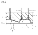
- the die has a portion, as required, electroplated through neutral-bathing to have a plating layer A of nickel-tungsten alloy having a thickness as required, as shown in Fig. 2.
- Plating layer A of nickel tungsten alloy is provided for example on the upper and lower cavities 3 and 4 internal surfaces, the resin channel 10 (cull 19 and runner and gate 20) internal surface, the air vent 18 surface, the concavity 7 surface, the pot 8 internal surface, the die's P. L plane, the plunger 9 external surface, the ejector pins 14 and 15 external surfaces, and the ejector pin fitting holes 16 and 17 internal surfaces.
- dies 1 and 2 are heated by heating means 11 and 12 to have a temperature at which resin is molded and also lead frame 6 having electronic component 5 molded thereto is fed to bottom die 2 and set at a predetermined position thereof and a resin material R is supplied into pot 8, and bottom die 2 is moved upward to close dies 1 and 2.
- upper and lower cavities 3 and 4 have electronic component 5 and lead frame 6 therearound fit therein.
- plunger 9 can apply pressure to the resin material heated and melted in pot 8, to inject the melted resin material into upper and lower cavities 3 and 4 and thus fill the cavities with the melted resin material and also to seal and thus mold electronic component 5 and lead frame 6 therearound in upper and lower cavities 3 and 4 to mold electronic component 5 and lead frame 6 therearound internal to resin-molded body 13 corresponding in geometry to upper and lower cavities 3 and 4.
- dies 1 and 2 are opened an ejector pins 14 and 15 are used to eject and thus release resin molded body 13 from upper and lower cavities 3 and 4.
- NiW nickel-tungsten alloy plating
- an initial, mold release force represents a minimal ejection force required to eject and thus release a resin-molded body from a die cavity.
- the die of the present embodiment is used for resin-sealing and molding, with a surface processed with NiW and thus allowing an initial, mold release force of an extremely small value, resin-molded body 13 can be efficiently released from die cavities 3 and 4 and the die can also be efficiently prevented from having resin flash adhering to its P.L plane and the like.
- resin molded body 13 can be efficiently released from die cavities 3 and 4 and resin flash remaining and thus adhering to the cavities can be removed readily and in a short period of time, a product can be produced at a high level of productivity.
- the die can be efficiently prevented from having resin flash adhering to its P.L plane and the like the aforementioned problems attributed to such resin flash (the resin flash affecting a size of a product and introduced into the product) can be resolved to provide a high quality product that is highly reliable.
- Table 2 represents a result of an experiment for microVickers hardness to estimate the hardness of a processed surface of each die that is obtained from the above experiment.
- microVickers hardness is an index representing a hardness of a die surface.
- a surface processed with HCr has a microVickers hardness of 1000 to 1100, whereas a surface processed with various NiW has a higher microVickers hardness.
- a surface processed with NiW with 40% by weight of W has a microVickers hardness of 1300 to 1400.
- the die of the present embodiment is used for resin-sealing and molding, it has a level of durability higher than a surface processed with HCr. As such, the die can be used for molding more frequently to produce products at a high level of productivity.
- plating layer A of nickel-tungsten alloy can be applied at least on the upper and lower cavities 3 and 4 internal surfaces.
- the pot 8 internal surface and the plunger 9 external surface are plated with nickel-tungsten alloy, there can be provided better releaseability between a surface processed with NiW and resin flash and the pot 8 internal surface and the plunger 9 external surface can thus be efficiently prevented from such resin flash from adhering thereto and the plunger can also be efficiently prevented from sliding improperly due to such resin flash.
- ejector pins 14 and 15 and the fitting holes 16 and 17 internal surfaces are plated with nickel-tungsten alloy, there can be provided better releaseability between a surface processed with NiW and resin flash and ejector pins 14 and 15 and the fitting holes 16 and 17 internal surfaces can thus be efficiently prevented from such resin flash adhering thereto and ejector pins 14 and 15 can also be efficiently prevented from sliding improperly due to such resin flash.
- the ejector pin can be dispensed with.
- the die provided with an ejector pin there can be provided better releaseability between a surface processed with NiW and a resin molded body or the like to readily extract the resin molded body from the die cavities.
- a high quality product that is highly reliable can be produced at a high level of productivity.
- thermosetting resin material it may alternatively use a thermoplastic resin material and various types of resin material.
- the present invention is applicable to a printed circuit board referred to as a so-called PC board of plastic and substrates of various types of material.
- a surface processed with HCr tends to have a dropping hardness
- a surface processed with NiW has a hardness with a low level of temperature dependency and it thus has a stable hardness.
- the surfaces were subjected to a scratching test, and a surface processed with HCr is readily abraded to expose a mother material of the die, whereas a surface processed with NiW, having a hard, intermediate diffusion layer, is not abraded to expose a mother material of the die so much as that processed with HCr.
- a surface processed with HCr readily cracks while the surface is thus processed, and in resin-molding, resin enters and cures for example in an undercut crack to degrade the releaseability of a resin-molded body.
- a surface processed with NiW hardly cracks and thus provides superior releaseability of a resin-molded body to a surface processed with HCr.
- a surface processed with NiW is higher in uniform electroconductivity than a surface processed with HCr. As such there can be reliably provided a plating layer having a uniform thickness for example of 5 ⁇ m.
- the embodiment employs a NiW layer having a thickness of 5 ⁇ m
- it can employ a NiW layer having a thickness no more than or no less than 5 ⁇ m.
- the NiW layer provided on the die surface (a die material) through electroplating is heated in the air and thus cured, although the NiW layer thus processed readily has a surface with an oxide film thereon and this requires a step of removing the oxide film.
- the heating and curing process is provided in a vacuum and gaseous nitrogen is also used to cool (the die material provided with the NiW layer) the die surface can be provided with a reliable NiW layer to eliminate the step of removing the oxide film.
- the surface can again be provided with a NiW layer and the die can also again provide resin-sealing and molding.
Landscapes
- Moulds For Moulding Plastics Or The Like (AREA)
- Encapsulation Of And Coatings For Semiconductor Or Solid State Devices (AREA)
- Electroplating And Plating Baths Therefor (AREA)
- Electroplating Methods And Accessories (AREA)
Abstract
Description
| i. | Die Temperature | 180°C |
| ii. | Injection Pressure | 9.807 MPa |
| iii. | Injection Rate | 21 mm/5 sec |
| iv. | Resin Material | epoxy resin (with no mold release agent added) |
| v. | Die Material | SKD-11 |
| vi. | Die Surface Processing | nickel-tungsten alloy plating (NiW), compared with hard chromium plating (HCr) |
| vii. | Thickness of the |
5 µm |


Claims (8)
- A die used for sealing and molding an electronic component (5) with a resin material (R), having a coating layer (A) of nickel-tungsten alloy on at least a surface thereof contacting a melted resin material when the resin is molded.
- The die of claim 1, wherein said coating layer (A) is a plating layer formed of a nickel-tungsten alloy containing at least 20% by weight of tungsten.
- The die of claim 2, wherein said coating layer (A) has a tungsten content of at most 60% by weight.
- The die of claim 1, wherein said coating layer (A) is 1 µm to 20 µm in thickness.
- The die of claim 1, comprising:wherein said coating layer (A) is provided on an internal surface of said upper and lower cavities, an internal surface of said resin channel, an internal surface of said concavity, an internal surface of said pot, the parting-line plane of each of said fixed die and said movable die, and an external surface of said plunger.a fixed die (1);a movable die (2) arranged opposite to the fixed die;upper and lower cavities (3, 4) provided in said fixed die and said movable die in their respective die planes to face each other along a parting-line plane of said fixed die and said movable die, for molding the resin;a concavity (7) receiving and setting a support (6) having the electronic component (5) mounted thereto;a pot (8) arranged at one of said fixed die and said movable die for supplying the resin material;a plunger (9) fit internal to the pot for applying pressure to the resin; anda resin channel (10) to allow said pot and said upper cavity (3) to communicate with each other for transporting the melted resin material,
- The die of claim 5, further comprising an ejector pin (14, 15) ejecting and releasing from said upper and lower cavities (3, 4) a resin-molded body (13) molded in said upper and lower cavities, and an ejector pin fitting hole (16, 17) fitting said ejector pin (14, 15) therein, wherein said ejector pin has an external surface provided with said coating layer (A) and/or said ejector pin fitting hole has an internal surface provided with said coating layer (A).
- The die of claim 5, wherein said resin channel (10) includes a cull (19) and a runner and gate (20) arranged opposite to said pot (8) for dispensing the melting resin, said cull and said runner and gate having an internal surface provided with said coating layer (A).
- The die of claim 5, further comprising an air vent (18) allowing said upper cavity (3) to communicate external to the die, said air vent having a surface provided with said coating layer (A).
Applications Claiming Priority (2)
| Application Number | Priority Date | Filing Date | Title |
|---|---|---|---|
| JP31759899A JP2001135659A (en) | 1999-11-09 | 1999-11-09 | Mold for resin molding of electronic parts |
| JP31759899 | 1999-11-09 |
Publications (2)
| Publication Number | Publication Date |
|---|---|
| EP1100122A2 true EP1100122A2 (en) | 2001-05-16 |
| EP1100122A3 EP1100122A3 (en) | 2004-01-21 |
Family
ID=18090010
Family Applications (1)
| Application Number | Title | Priority Date | Filing Date |
|---|---|---|---|
| EP00309855A Withdrawn EP1100122A3 (en) | 1999-11-09 | 2000-11-06 | Die used for resin-sealing and molding an electronic component |
Country Status (6)
| Country | Link |
|---|---|
| US (1) | US6773247B1 (en) |
| EP (1) | EP1100122A3 (en) |
| JP (1) | JP2001135659A (en) |
| KR (1) | KR20010070199A (en) |
| SG (1) | SG101432A1 (en) |
| TW (1) | TW518698B (en) |
Families Citing this family (18)
| Publication number | Priority date | Publication date | Assignee | Title |
|---|---|---|---|---|
| US6001672A (en) * | 1997-02-25 | 1999-12-14 | Micron Technology, Inc. | Method for transfer molding encapsulation of a semiconductor die with attached heat sink |
| AUPR244801A0 (en) * | 2001-01-10 | 2001-02-01 | Silverbrook Research Pty Ltd | A method and apparatus (WSM01) |
| US7220615B2 (en) * | 2001-06-11 | 2007-05-22 | Micron Technology, Inc. | Alternative method used to package multimedia card by transfer molding |
| US6969918B1 (en) * | 2001-08-30 | 2005-11-29 | Micron Technology, Inc. | System for fabricating semiconductor components using mold cavities having runners configured to minimize venting |
| JP5208500B2 (en) * | 2004-05-06 | 2013-06-12 | エヌエックスピー ビー ヴィ | Assembling method and assembly produced by this method |
| KR100661530B1 (en) | 2005-02-25 | 2006-12-27 | 대양전기공업 주식회사 | Electric Reflector Plating Method and Plating Equipment |
| JP4854493B2 (en) * | 2006-12-15 | 2012-01-18 | 日本プレーテック株式会社 | Injection mold |
| TW200830573A (en) * | 2007-01-03 | 2008-07-16 | Harvatek Corp | Mold structure for packaging light-emitting diode chip and method for packaging light-emitting diode chip |
| KR20090107686A (en) * | 2008-04-10 | 2009-10-14 | 삼성전자주식회사 | Injection molding machine |
| JP4789971B2 (en) * | 2008-05-08 | 2011-10-12 | 本田技研工業株式会社 | Mold and manufacturing method thereof |
| US8257075B2 (en) * | 2008-11-10 | 2012-09-04 | Apple Inc. | Carbon composite mold design |
| KR20110081634A (en) * | 2010-01-08 | 2011-07-14 | 삼성전자주식회사 | Semiconductor encapsulant forming apparatus and molding method |
| JP5583487B2 (en) * | 2010-06-14 | 2014-09-03 | 矢崎総業株式会社 | Fuse unit, mold structure, and molding method using mold structure |
| US20140275915A1 (en) * | 2013-03-13 | 2014-09-18 | Medtronic, Inc. | Implantable medical device including a molded planar transformer |
| JP2020536177A (en) | 2017-09-28 | 2020-12-10 | マクステリアル インコーポレイテッド | Articles containing surface coatings and methods for producing them |
| CN112476868B (en) * | 2020-10-27 | 2022-03-18 | 北京理工大学 | Method for controlling temperature and performance of precision mold and precision mold |
| EP4355933A4 (en) | 2021-06-18 | 2026-01-07 | Maxterial Inc | COATED SURFACES, COATINGS AND ITEMS WITH IT |
| KR20260012186A (en) * | 2022-12-16 | 2026-01-26 | 맥스터리얼, 인크. | Molds and dies including surface coatings |
Family Cites Families (9)
| Publication number | Priority date | Publication date | Assignee | Title |
|---|---|---|---|---|
| JPS56141922A (en) | 1980-04-04 | 1981-11-05 | World Metal:Kk | Metallic mold formed alloy layer for molding |
| JPS58212840A (en) * | 1982-06-03 | 1983-12-10 | Mishima Kosan Co Ltd | Casting mold for continuous casting |
| JP2649685B2 (en) | 1988-03-16 | 1997-09-03 | トーワ株式会社 | Mold for resin molding of electronic parts |
| JPH03104874A (en) | 1989-09-14 | 1991-05-01 | Toowa Kk | Method for constituting electroless nickel plating layer on metallic mold surface and metallic mold for resin sealing of electronic parts |
| KR920000977A (en) | 1990-06-18 | 1992-01-29 | 한형수 | Nickel-tungsten plating method of high temperature mold |
| JPH08309803A (en) | 1995-05-15 | 1996-11-26 | Towa Kk | Mold for resin molding |
| JPH10202698A (en) | 1997-01-29 | 1998-08-04 | Sekisui Chem Co Ltd | Injection mold |
| JPH10286845A (en) | 1997-04-15 | 1998-10-27 | Seiko Epson Corp | Resin sealing mold and method of manufacturing resin sealed semiconductor device |
| TW421833B (en) * | 1998-07-10 | 2001-02-11 | Apic Yamada Corp | Method of manufacturing semiconductor devices and resin molding machine |
-
1999
- 1999-11-09 JP JP31759899A patent/JP2001135659A/en not_active Withdrawn
-
2000
- 2000-11-02 US US09/705,237 patent/US6773247B1/en not_active Expired - Fee Related
- 2000-11-06 SG SG200006390A patent/SG101432A1/en unknown
- 2000-11-06 EP EP00309855A patent/EP1100122A3/en not_active Withdrawn
- 2000-11-08 TW TW089123635A patent/TW518698B/en not_active IP Right Cessation
- 2000-11-09 KR KR1020000066349A patent/KR20010070199A/en not_active Ceased
Also Published As
| Publication number | Publication date |
|---|---|
| TW518698B (en) | 2003-01-21 |
| JP2001135659A (en) | 2001-05-18 |
| US6773247B1 (en) | 2004-08-10 |
| KR20010070199A (en) | 2001-07-25 |
| EP1100122A3 (en) | 2004-01-21 |
| SG101432A1 (en) | 2004-01-30 |
Similar Documents
| Publication | Publication Date | Title |
|---|---|---|
| US6773247B1 (en) | Die used for resin-sealing and molding an electronic component | |
| KR100929054B1 (en) | Method of Resin Encapsulation, Apparatus for Resin Encapsulation, Method of Manufacturing Semiconductor Device, Semiconductor Device and Resin Material | |
| US6309916B1 (en) | Method of molding plastic semiconductor packages | |
| KR101311014B1 (en) | Compression molding method and compression mold for semiconductor chip | |
| EP1035572A3 (en) | Method of coating semiconductor wafer with resin and mold used therefor | |
| EP0713248A2 (en) | Molding method and apparatus | |
| EP2447986B1 (en) | Resin encapsulation molding method and apparatus for electrical circuit component | |
| CN100433280C (en) | Resin-sealed semiconductor package, method and apparatus for manufacturing the same | |
| JP2626971B2 (en) | Resin encapsulation molding method and mold for electronic parts | |
| EP1768168A2 (en) | Method of resin seal moulding electronic component and apparatus therefor | |
| CN100536100C (en) | Resin sealing shaping device for electronic parts | |
| EP1768167A2 (en) | Method of resin-seal molding electronic component and apparatus therefor. | |
| US6447707B1 (en) | Molding method of thermosetting resin and mold with unnecessary gap heating | |
| JPH0246134B2 (en) | ||
| JP4755068B2 (en) | Resin sealing mold for electronic parts | |
| JPH10272655A (en) | Resin sealing mold | |
| JP3444747B2 (en) | Resin sealing molding method for electronic parts | |
| JP2649685B2 (en) | Mold for resin molding of electronic parts | |
| JP3093899B2 (en) | Mold for resin molding of electronic parts | |
| JP2998077B2 (en) | Resin encapsulation molding method and mold for electronic parts | |
| JPH03104874A (en) | Method for constituting electroless nickel plating layer on metallic mold surface and metallic mold for resin sealing of electronic parts | |
| JPH11300781A (en) | Molding method for resin and mold equipment for molding | |
| JPH01299008A (en) | Molding device | |
| GB2155843A (en) | Promoting mold release of molded objects | |
| JPS6255112A (en) | Plunger for multi-plungers type resin molding apparatus |
Legal Events
| Date | Code | Title | Description |
|---|---|---|---|
| PUAI | Public reference made under article 153(3) epc to a published international application that has entered the european phase |
Free format text: ORIGINAL CODE: 0009012 |
|
| AK | Designated contracting states |
Kind code of ref document: A2 Designated state(s): AT BE CH CY DE DK ES FI FR GB GR IE IT LI LU MC NL PT SE TR |
|
| AX | Request for extension of the european patent |
Free format text: AL;LT;LV;MK;RO;SI |
|
| PUAL | Search report despatched |
Free format text: ORIGINAL CODE: 0009013 |
|
| AK | Designated contracting states |
Kind code of ref document: A3 Designated state(s): AT BE CH CY DE DK ES FI FR GB GR IE IT LI LU MC NL PT SE TR |
|
| AX | Request for extension of the european patent |
Extension state: AL LT LV MK RO SI |
|
| 17P | Request for examination filed |
Effective date: 20040213 |
|
| AKX | Designation fees paid |
Designated state(s): DE GB NL |
|
| STAA | Information on the status of an ep patent application or granted ep patent |
Free format text: STATUS: THE APPLICATION HAS BEEN WITHDRAWN |
|
| 18W | Application withdrawn |
Effective date: 20051021 |