EP1100113A2 - Lampe à décharge à barrière diélectrique - Google Patents
Lampe à décharge à barrière diélectrique Download PDFInfo
- Publication number
- EP1100113A2 EP1100113A2 EP00123542A EP00123542A EP1100113A2 EP 1100113 A2 EP1100113 A2 EP 1100113A2 EP 00123542 A EP00123542 A EP 00123542A EP 00123542 A EP00123542 A EP 00123542A EP 1100113 A2 EP1100113 A2 EP 1100113A2
- Authority
- EP
- European Patent Office
- Prior art keywords
- dielectric barrier
- discharge lamp
- barrier discharge
- casing
- lamp device
- Prior art date
- Legal status (The legal status is an assumption and is not a legal conclusion. Google has not performed a legal analysis and makes no representation as to the accuracy of the status listed.)
- Granted
Links
Images


Classifications
-
- H—ELECTRICITY
- H01—ELECTRIC ELEMENTS
- H01J—ELECTRIC DISCHARGE TUBES OR DISCHARGE LAMPS
- H01J65/00—Lamps without any electrode inside the vessel; Lamps with at least one main electrode outside the vessel
-
- H—ELECTRICITY
- H05—ELECTRIC TECHNIQUES NOT OTHERWISE PROVIDED FOR
- H05G—X-RAY TECHNIQUE
- H05G2/00—Apparatus or processes specially adapted for producing X-rays, not involving X-ray tubes, e.g. involving generation of a plasma
- H05G2/001—X-ray radiation generated from plasma
- H05G2/003—X-ray radiation generated from plasma being produced from a liquid or gas
-
- H—ELECTRICITY
- H01—ELECTRIC ELEMENTS
- H01J—ELECTRIC DISCHARGE TUBES OR DISCHARGE LAMPS
- H01J65/00—Lamps without any electrode inside the vessel; Lamps with at least one main electrode outside the vessel
- H01J65/04—Lamps in which a gas filling is excited to luminesce by an external electromagnetic field or by external corpuscular radiation, e.g. for indicating plasma display panels
-
- H—ELECTRICITY
- H01—ELECTRIC ELEMENTS
- H01L—SEMICONDUCTOR DEVICES NOT COVERED BY CLASS H10
- H01L21/00—Processes or apparatus adapted for the manufacture or treatment of semiconductor or solid state devices or of parts thereof
- H01L21/67—Apparatus specially adapted for handling semiconductor or electric solid state devices during manufacture or treatment thereof; Apparatus specially adapted for handling wafers during manufacture or treatment of semiconductor or electric solid state devices or components ; Apparatus not specifically provided for elsewhere
- H01L21/67005—Apparatus not specifically provided for elsewhere
- H01L21/67011—Apparatus for manufacture or treatment
- H01L21/67098—Apparatus for thermal treatment
- H01L21/67115—Apparatus for thermal treatment mainly by radiation
-
- H—ELECTRICITY
- H05—ELECTRIC TECHNIQUES NOT OTHERWISE PROVIDED FOR
- H05B—ELECTRIC HEATING; ELECTRIC LIGHT SOURCES NOT OTHERWISE PROVIDED FOR; CIRCUIT ARRANGEMENTS FOR ELECTRIC LIGHT SOURCES, IN GENERAL
- H05B3/00—Ohmic-resistance heating
- H05B3/02—Details
- H05B3/04—Waterproof or air-tight seals for heaters
Definitions
- This invention relates to a dielectric barrier discharge lamp device.
- a dielectric barrier discharge lamp 2 of a substantially hollow cylindrical shape is comprised of a discharge container 21 made of quartz having an entire length of about 300 mm.
- a discharge space is enclosed between an inner tube 22 and an outer tube 23 which are arranged coaxially.
- the inner tube 22 has an inner diameter D1 of 12 to 15 mm and the outer tube 23 has an outer diameter D2 of 24 to 27 mm.
- the outer surfaces of the inner tube 22 and the outer tube 23 are provided with electrodes 24, 25 made of a metallic net for allowing light to pass therethrough.
- a dielectric barrier discharge lamp device used in connection with such a dielectric barrier discharge lamp as described above is constructed such that a plurality of dielectric barrier discharge lamps 2 are arranged in one casing 10. Light radiated from each of the dielectric barrier discharge lamps 2 passes through a glass window 3 arranged in the casing 10 and is radiated onto a processed item W (hereinafter also called a workpiece).
- the dielectric barrier discharge lamps 2 are arranged in a space sealed hermetically by the casing 10 and the window 3.
- a cooling block 4 is used for cooling the dielectric barrier discharge lamps 2, and a cooling pipe 6 for cooling medium is used for cooling the cooling block 4. Further, mirrors 5 are arranged for reflecting light radiated from the dielectric barrier discharge lamps 2.
- the present invention has been made in view of the foregoing circumstances, and it is an object of the present invention to provide a dielectric barrier discharge lamp device for uniformly emitting ultraviolet rays on a processed item having an increased surface area. According to a further object, the dielectric barrier discharge lamp device should be easily adaptable to the size of the processed item by merely changing the number of casings containing the dielectric barrier discharge lamps in response to the size of the processed item.
- the dielectric barrier discharge lamp device of the invention is characterized in that at least one dielectric barrier discharge lamp is arranged in a hermetically sealed casing, said casing comprising a hollow longitudinally extending main part being closed at both ends by end parts, at least a portion of said main part of the casing defining a window allowing light radiated from the at least one dielectric barrier discharge lamp to pass therethrough onto the workpiece.
- At least one end part of the casing is provided with a passage allowing inert gas to be introduced into the casing. Further, at least one of the end parts is adapted such as to allow loading or unloading of the at least one dielectric barrier discharge lamp.
- a plurality of casings are arranged side by side with their windows facing the workpiece to be irradiated.
- the number of casings having the at least one dielectric barrier discharge lamp arranged therein is correspondingly increased so that a large-size integral window is not required and the size of the window of each of the casings need not be increased.
- a relatively small window having a high and uniform transmission factor can be used for each of the casings, and the intensity of ultraviolet rays on the processed item can be made uniform.
- the dielectric barrier discharge lamp device can be easily adapted to the size of the processed item by merely changing the number of casings.
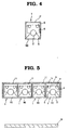
- Fig.3 is an illustrative view showing an example of a casing of the dielectric barrier discharge lamp device of the present invention.
- Fig.4 is a sectional view taken along line A-A shown in Fig.3.
- the dielectric barrier discharge lamp 2 is similar to that shown in Fig.1, wherein a discharge container 21 has a longitudinal length of about 600 mm and the remaining reference numerals denote the same elements as in Fig. 1.
- the mirror for reflecting light radiated from the dielectric barrier discharge lamp 2 is not shown in Fig. 3 for sake of clarity.
- the casing 1 is constituted by a longitudinally extending side wall 11 as the main part of the casing and end walls 12 as the end parts arranged at both ends of the side wall.
- the side wall 11 has a hollow pillar-like shape and is entirely made of quartz glass. It has a square cross-section and its outer shape is rectangular having a longitudinal size of 60 mm, a lateral size of 60 mm and a length of 650 mm.
- the end walls 12 are made of a metallic block of aluminum.
- a cooling pipe 6 for passage of cooling fluid for cooling the dielectric barrier discharge lamp 2 stored in the casing 1 extends through one end wall 12.
- This cooling pipe 6 is of a U-shape with the crossbeam arranged within the casing 1 and the shanks passing through the end wall 12.
- the cooling pipe 6 also passes through the cooling block 4 which is in contact with the outer tube 23 of the dielectric barrier discharge lamp 2 and so cools the cooling block 4 and also the dielectric barrier discharge lamp 2.
- the other end wall 12 is comprised of a cylindrical part 121 having substantially the same shape as the outer shape of the side wall 11 and an opening or closing part 122 which may function as a door for use in loading or unloading the dielectric barrier discharge lamp 2 into or out of the casing 1.
- cylindrical part 121 has a connector 9 connected to a lead wire 8 for applying a voltage to the dielectric barrier discharge lamp 2 at a location opposite to the window 110.
- the end walls 12 are fixed to the side wall 11 by O-rings 7 so that the end walls 12 are hermetically connected to both ends of the longitudinally extending side wall 11 resulting in a casing 1 which is hermetically sealed.
- end walls 12 of the casing 1 are provided with flow passages 12a for nitrogen gas or some other inert gas so that the inside of the casing 1 can be purged with nitrogen through the flow passages 12a.
- the flow passages 12a are provided with a coupler T and connected to a gas flow pipe not shown in the figure.
- the nitrogen gas introduced through one flow passage 12a is discharged out of the other flow passage 12a, the inside of the casing 1 is purged with nitrogen and vacuum ultraviolet light emitted by the dielectric barrier discharge lamp is radiated against the processed item without being absorbed in the casing 1.
- one dielectric barrier discharge lamp 2 is stored in the casing 1, and the entire side wall 11 is made of quartz glass for allowing ultraviolet rays to pass therethrough and one surface of the side wall 11 is used as a window 110.
- the side wall 11 may be made of metal or any other suitable material which does not allow ultraviolet rays to pass.
- a window for passage of the ultraviolet rays is arranged at one surface of the side wall 11.
- a glass component is applied as this window.
- a plurality of casings 1 having a dielectric barrier discharge lamp 2 arranged therein is combined to the dielectric barrier discharge lamp device of the invention in accordance with the size of the item W to be processed, i.e. the processing area of the processed item W, in such a way that the window 110 of the casing 1 faces toward the processed item W.
- four casings are arranged side by side in accordance with a common processing area of the processed item.
- a coupling case (or outer casing) K is applied as means for arranging the casings 1 side by side.
- the means for side-by-side assembly of the casings 1 within the coupling case K is not particularly limited, and any kind of suitable means may be applied.
- the dielectric barrier discharge lamp device when an item or workpiece W having a large surface area, respectively a large processing area, is to be processed, it is only necessary that the number of the casings 1 having a dielectric barrier discharge lamp 2 arranged therein be chosen in correspondence with this area. It is no longer necessary to prepare a large-size integral window as in the prior art.
- the size of the window 110 in each of the casings 1 need not be increased, and the window 110 of each of the casings can be prepared such as to have a uniform transmission factor resulting in a uniform illumination of the processed item even if the processing area is increased.
- the invention provides a dielectric barrier discharge lamp device capable of easily being adapted to the size of any workpiece to be processed.
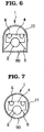
- Figs.6 and 7 illustrate another example of a casing in which a dielectric barrier discharge lamp is stored.
- Fig.6 shows a case in which the side wall 11 of the casing 1 is made of quartz glass and its sectional shape is dome-like (i.e., one side of the casing is planar and the other portions are curved and have an arcuate shape).
- Fig.7 shows an example in which the side wall 11 of the casing 1 is a quartz glass tube having a circular cross-section. A part of the side wall 11 is used as a window 110 through which light from the dielectric barrier discharge lamp permeates.
- the quartz glass pipe as such can be utilized as a casing so that the casing can be easily manufactured.
- each of the casings 1 has a cooling block 4 and a cooling pipe 6 for cooling the dielectric barrier discharge lamp 2 and a mirror 5 arranged therein.
- the invention is not limited to the specific casings described above but various modifications can be made. Further, although it is preferred to arrange only one lamp within each casing, more than one lamp per casing may be used as well and the invention is not limited to the lamps explicitly described in connection with Fig. 1.
Applications Claiming Priority (2)
| Application Number | Priority Date | Filing Date | Title |
|---|---|---|---|
| JP31215599A JP3591393B2 (ja) | 1999-11-02 | 1999-11-02 | 誘電体バリア放電ランプ装置 |
| JP31215599 | 1999-11-02 |
Publications (3)
| Publication Number | Publication Date |
|---|---|
| EP1100113A2 true EP1100113A2 (fr) | 2001-05-16 |
| EP1100113A3 EP1100113A3 (fr) | 2006-05-10 |
| EP1100113B1 EP1100113B1 (fr) | 2014-09-10 |
Family
ID=18025913
Family Applications (1)
| Application Number | Title | Priority Date | Filing Date |
|---|---|---|---|
| EP00123542.3A Expired - Lifetime EP1100113B1 (fr) | 1999-11-02 | 2000-10-27 | Lampe à décharge à barrière diélectrique |
Country Status (5)
| Country | Link |
|---|---|
| US (1) | US6657367B1 (fr) |
| EP (1) | EP1100113B1 (fr) |
| JP (1) | JP3591393B2 (fr) |
| KR (1) | KR100470934B1 (fr) |
| TW (1) | TW457513B (fr) |
Cited By (5)
| Publication number | Priority date | Publication date | Assignee | Title |
|---|---|---|---|---|
| US6501084B1 (en) * | 1999-03-31 | 2002-12-31 | Toyoda Gosei Co., Ltd. | Lamp unit using short-wave light emitting device |
| EP1298965A2 (fr) * | 2001-08-07 | 2003-04-02 | Nikon Corporation | Dispositifs d'émission de rayonnement utilisant plusieures sources à plasma de décharge et appareils et procédés pour microlithographie qui les utilisent |
| US20150274548A1 (en) * | 2012-10-19 | 2015-10-01 | Fraunhofer-Gesellschaft zur Förderung der angewandten Forschung e.V. | UV Light Source Having Combined Ionization and Formation of Excimers |
| KR20170140438A (ko) * | 2010-01-18 | 2017-12-20 | 엘지전자 주식회사 | 무선 통신 시스템에서 채널 품질 정보를 제공하는 방법 및 장치 |
| WO2019061547A1 (fr) * | 2017-09-30 | 2019-04-04 | 王恩珮 | Lampe à support imperméable cascadable |
Families Citing this family (2)
| Publication number | Priority date | Publication date | Assignee | Title |
|---|---|---|---|---|
| EP1873810A1 (fr) * | 2005-04-22 | 2008-01-02 | Hoya Candeo Optronics Corporation | Lampe a excimere |
| US8022377B2 (en) * | 2008-04-22 | 2011-09-20 | Applied Materials, Inc. | Method and apparatus for excimer curing |
Family Cites Families (16)
| Publication number | Priority date | Publication date | Assignee | Title |
|---|---|---|---|---|
| US3872349A (en) * | 1973-03-29 | 1975-03-18 | Fusion Systems Corp | Apparatus and method for generating radiation |
| US3994073A (en) * | 1975-04-08 | 1976-11-30 | Ppg Industries, Inc. | Air cooling means for UV processor |
| JP2693419B2 (ja) * | 1986-01-22 | 1997-12-24 | 株式会社東芝 | カラー受像装置 |
| US4933602A (en) * | 1987-03-11 | 1990-06-12 | Hitachi, Ltd. | Apparatus for generating light by utilizing microwave |
| US5051663A (en) * | 1990-03-26 | 1991-09-24 | Fusion Systems Corporation | Electrodeless lamp with improved bulb mounting arrangement |
| EP0482230B1 (fr) * | 1990-10-22 | 1995-06-21 | Heraeus Noblelight GmbH | Dispositif de rayonnement à haute puissance |
| US5751327A (en) * | 1993-06-18 | 1998-05-12 | Xeikon N.V. | Printer including temperature controlled LED recording heads |
| JP3025414B2 (ja) * | 1994-09-20 | 2000-03-27 | ウシオ電機株式会社 | 誘電体バリア放電ランプ装置 |
| JP3127750B2 (ja) * | 1994-10-25 | 2001-01-29 | ウシオ電機株式会社 | 誘電体バリア放電ランプ装置 |
| JPH08124540A (ja) * | 1994-10-25 | 1996-05-17 | Ushio Inc | キセノン照射装置とそれを用いた物体表面改質装置 |
| JP3502498B2 (ja) * | 1996-01-22 | 2004-03-02 | 大日本スクリーン製造株式会社 | 基板処理装置 |
| JP3526691B2 (ja) * | 1996-05-14 | 2004-05-17 | ウシオ電機株式会社 | 紫外線照射装置および紫外線処理装置 |
| JP3324428B2 (ja) * | 1996-11-20 | 2002-09-17 | ウシオ電機株式会社 | フォトレジストの表面処理装置 |
| JP3314656B2 (ja) * | 1997-04-11 | 2002-08-12 | ウシオ電機株式会社 | 光源装置 |
| JPH1144799A (ja) * | 1997-05-27 | 1999-02-16 | Ushio Inc | 光路分割型紫外線照射装置 |
| JP2000011960A (ja) * | 1998-06-18 | 2000-01-14 | Hooya Shot Kk | 誘電体バリア放電ランプを用いた表面処理装置及び方法 |
-
1999
- 1999-11-02 JP JP31215599A patent/JP3591393B2/ja not_active Expired - Lifetime
-
2000
- 2000-08-25 TW TW089117287A patent/TW457513B/zh not_active IP Right Cessation
- 2000-10-27 EP EP00123542.3A patent/EP1100113B1/fr not_active Expired - Lifetime
- 2000-11-02 KR KR10-2000-0064872A patent/KR100470934B1/ko active IP Right Grant
- 2000-11-02 US US09/703,596 patent/US6657367B1/en not_active Expired - Lifetime
Non-Patent Citations (1)
| Title |
|---|
| None |
Cited By (7)
| Publication number | Priority date | Publication date | Assignee | Title |
|---|---|---|---|---|
| US6501084B1 (en) * | 1999-03-31 | 2002-12-31 | Toyoda Gosei Co., Ltd. | Lamp unit using short-wave light emitting device |
| EP1298965A2 (fr) * | 2001-08-07 | 2003-04-02 | Nikon Corporation | Dispositifs d'émission de rayonnement utilisant plusieures sources à plasma de décharge et appareils et procédés pour microlithographie qui les utilisent |
| EP1298965A3 (fr) * | 2001-08-07 | 2004-07-28 | Nikon Corporation | Dispositifs d'émission de rayonnement utilisant plusieures sources à plasma de décharge et appareils et procédés pour microlithographie qui les utilisent |
| KR20170140438A (ko) * | 2010-01-18 | 2017-12-20 | 엘지전자 주식회사 | 무선 통신 시스템에서 채널 품질 정보를 제공하는 방법 및 장치 |
| US20150274548A1 (en) * | 2012-10-19 | 2015-10-01 | Fraunhofer-Gesellschaft zur Förderung der angewandten Forschung e.V. | UV Light Source Having Combined Ionization and Formation of Excimers |
| US9718705B2 (en) * | 2012-10-19 | 2017-08-01 | Fraunhofer-Gesellschaft zur Förderung der angewandten Forschung e.V. | UV light source having combined ionization and formation of excimers |
| WO2019061547A1 (fr) * | 2017-09-30 | 2019-04-04 | 王恩珮 | Lampe à support imperméable cascadable |
Also Published As
| Publication number | Publication date |
|---|---|
| US6657367B1 (en) | 2003-12-02 |
| JP3591393B2 (ja) | 2004-11-17 |
| EP1100113B1 (fr) | 2014-09-10 |
| EP1100113A3 (fr) | 2006-05-10 |
| TW457513B (en) | 2001-10-01 |
| KR20010051405A (ko) | 2001-06-25 |
| KR100470934B1 (ko) | 2005-02-21 |
| JP2001135279A (ja) | 2001-05-18 |
Similar Documents
| Publication | Publication Date | Title |
|---|---|---|
| EP3457430B1 (fr) | Lampe étanche avec doubles zones de focalisation commandée par un laser | |
| US5581152A (en) | Dielectric barrier discharge lamp | |
| US10504714B2 (en) | Dual parabolic laser driven sealed beam lamp | |
| EP3540760B1 (fr) | Tube mécaniquement scellé pour lampe à plasma maintenu par laser et son procédé de production | |
| US20020030453A1 (en) | High brightness microwave lamp | |
| EP1564851A1 (fr) | Laser excimère à halogénure de gaz rare avec déflecteurs de gaz | |
| US6657367B1 (en) | Dielectric barrier discharge lamp device | |
| JP7361748B2 (ja) | 安定性の改善されたレーザ駆動封止ビームランプ | |
| US10186416B2 (en) | Apparatus and a method for operating a variable pressure sealed beam lamp | |
| KR20020006033A (ko) | 고압 방전 램프와 점화 안테나를 포함하는 유닛 | |
| US20050236997A1 (en) | Dielectric barrier discharge lamp having outer electrodes and illumination system having this lamp | |
| EP0780881B1 (fr) | Lampe à décharge sans électrodes | |
| JP2934511B2 (ja) | コロナ放電光源セル及びコロナ放電光源装置 | |
| EP1047110B1 (fr) | Lampe fluorescente et procedé pour sa fabrication | |
| JP3533918B2 (ja) | 光源装置 | |
| WO2018081220A1 (fr) | Appareil et procédé permettant de faire fonctionner une lampe à faisceau scellée à pression variable | |
| JP2005019229A (ja) | 誘電体バリア放電ランプ |
Legal Events
| Date | Code | Title | Description |
|---|---|---|---|
| PUAI | Public reference made under article 153(3) epc to a published international application that has entered the european phase |
Free format text: ORIGINAL CODE: 0009012 |
|
| AK | Designated contracting states |
Kind code of ref document: A2 Designated state(s): AT BE CH CY DE DK ES FI FR GB GR IE IT LI LU MC NL PT SE |
|
| AX | Request for extension of the european patent |
Free format text: AL;LT;LV;MK;RO;SI |
|
| PUAL | Search report despatched |
Free format text: ORIGINAL CODE: 0009013 |
|
| AK | Designated contracting states |
Kind code of ref document: A3 Designated state(s): AT BE CH CY DE DK ES FI FR GB GR IE IT LI LU MC NL PT SE |
|
| AX | Request for extension of the european patent |
Extension state: AL LT LV MK RO SI |
|
| RIC1 | Information provided on ipc code assigned before grant |
Ipc: G21K 5/00 20060101ALI20060323BHEP Ipc: B01J 19/12 20060101ALI20060323BHEP Ipc: H01J 65/04 20060101AFI20010321BHEP Ipc: H01J 61/52 20060101ALI20060323BHEP Ipc: H01L 21/00 20060101ALI20060323BHEP |
|
| 17P | Request for examination filed |
Effective date: 20060502 |
|
| AKX | Designation fees paid |
Designated state(s): DE GB NL |
|
| 17Q | First examination report despatched |
Effective date: 20091005 |
|
| RIC1 | Information provided on ipc code assigned before grant |
Ipc: H05B 3/04 20060101ALI20140512BHEP Ipc: H05G 2/00 20060101ALI20140512BHEP Ipc: H01L 21/67 20060101ALI20140512BHEP Ipc: H01J 61/52 20060101ALI20140512BHEP Ipc: H01J 65/04 20060101AFI20140512BHEP Ipc: B01J 19/12 20060101ALI20140512BHEP Ipc: G21K 5/00 20060101ALI20140512BHEP |
|
| GRAP | Despatch of communication of intention to grant a patent |
Free format text: ORIGINAL CODE: EPIDOSNIGR1 |
|
| GRAS | Grant fee paid |
Free format text: ORIGINAL CODE: EPIDOSNIGR3 |
|
| INTG | Intention to grant announced |
Effective date: 20140707 |
|
| GRAA | (expected) grant |
Free format text: ORIGINAL CODE: 0009210 |
|
| AK | Designated contracting states |
Kind code of ref document: B1 Designated state(s): DE GB NL |
|
| REG | Reference to a national code |
Ref country code: GB Ref legal event code: FG4D |
|
| REG | Reference to a national code |
Ref country code: DE Ref legal event code: R096 Ref document number: 60048714 Country of ref document: DE Effective date: 20141023 |
|
| REG | Reference to a national code |
Ref country code: NL Ref legal event code: T3 |
|
| REG | Reference to a national code |
Ref country code: DE Ref legal event code: R097 Ref document number: 60048714 Country of ref document: DE |
|
| PLBE | No opposition filed within time limit |
Free format text: ORIGINAL CODE: 0009261 |
|
| STAA | Information on the status of an ep patent application or granted ep patent |
Free format text: STATUS: NO OPPOSITION FILED WITHIN TIME LIMIT |
|
| 26N | No opposition filed |
Effective date: 20150611 |
|
| PGFP | Annual fee paid to national office [announced via postgrant information from national office to epo] |
Ref country code: NL Payment date: 20160913 Year of fee payment: 17 |
|
| PGFP | Annual fee paid to national office [announced via postgrant information from national office to epo] |
Ref country code: GB Payment date: 20161026 Year of fee payment: 17 |
|
| REG | Reference to a national code |
Ref country code: NL Ref legal event code: MM Effective date: 20171101 |
|
| GBPC | Gb: european patent ceased through non-payment of renewal fee |
Effective date: 20171027 |
|
| PG25 | Lapsed in a contracting state [announced via postgrant information from national office to epo] |
Ref country code: GB Free format text: LAPSE BECAUSE OF NON-PAYMENT OF DUE FEES Effective date: 20171027 Ref country code: NL Free format text: LAPSE BECAUSE OF NON-PAYMENT OF DUE FEES Effective date: 20171101 |
|
| PGFP | Annual fee paid to national office [announced via postgrant information from national office to epo] |
Ref country code: DE Payment date: 20191015 Year of fee payment: 20 |
|
| REG | Reference to a national code |
Ref country code: DE Ref legal event code: R071 Ref document number: 60048714 Country of ref document: DE |