EP1099952A1 - Schaltungszelle mit eingebauter Selbsttestfunktion und Verfahren zum Testen hierfür - Google Patents
Schaltungszelle mit eingebauter Selbsttestfunktion und Verfahren zum Testen hierfür Download PDFInfo
- Publication number
- EP1099952A1 EP1099952A1 EP00121371A EP00121371A EP1099952A1 EP 1099952 A1 EP1099952 A1 EP 1099952A1 EP 00121371 A EP00121371 A EP 00121371A EP 00121371 A EP00121371 A EP 00121371A EP 1099952 A1 EP1099952 A1 EP 1099952A1
- Authority
- EP
- European Patent Office
- Prior art keywords
- test
- circuit
- memory control
- control unit
- test pattern
- Prior art date
- Legal status (The legal status is an assumption and is not a legal conclusion. Google has not performed a legal analysis and makes no representation as to the accuracy of the status listed.)
- Granted
Links
Images


Classifications
-
- G—PHYSICS
- G06—COMPUTING OR CALCULATING; COUNTING
- G06F—ELECTRIC DIGITAL DATA PROCESSING
- G06F11/00—Error detection; Error correction; Monitoring
- G06F11/22—Detection or location of defective computer hardware by testing during standby operation or during idle time, e.g. start-up testing
- G06F11/2205—Detection or location of defective computer hardware by testing during standby operation or during idle time, e.g. start-up testing using arrangements specific to the hardware being tested
- G06F11/2236—Detection or location of defective computer hardware by testing during standby operation or during idle time, e.g. start-up testing using arrangements specific to the hardware being tested to test CPU or processors
-
- G—PHYSICS
- G01—MEASURING; TESTING
- G01R—MEASURING ELECTRIC VARIABLES; MEASURING MAGNETIC VARIABLES
- G01R31/00—Arrangements for testing electric properties; Arrangements for locating electric faults; Arrangements for electrical testing characterised by what is being tested not provided for elsewhere
- G01R31/28—Testing of electronic circuits, e.g. by signal tracer
- G01R31/317—Testing of digital circuits
- G01R31/3181—Functional testing
- G01R31/3185—Reconfiguring for testing, e.g. LSSD, partitioning
- G01R31/318505—Test of Modular systems, e.g. Wafers, MCM's
Definitions
- the invention relates to a method for testing circuit cells, through which a self-test circuit is modular can be, and circuit cells with built-in Self test function.
- the test procedure can be used for modular systems Circuits are used.
- US 5,422,643 describes a printed circuit board with several integrated circuits and a method mounted thereon for testing the integrated on the printed circuit board Circuits.
- the integrated circuits have one main circuit component each, test circuits, a latch circuit and a system interface, which the data input and the data output to the test circuits controls.
- the test circuits are circuitry-related identical to the main circuit component and with this and the system interface each via one Bus connected.
- Integrated circuits are made after manufacturing one Test procedure for testing the logical and dynamic behavior subjected to faulty circuits on the one hand recognize and on the other hand the performance based on the test results the integrated circuits.
- the Integrated circuits consist of a large number of logic Components that in turn consist of switching elements or Transistors exist. Highly complex integrated circuits have up to 100,000,000 switching elements or transistors on.
- Known test methods use stimulation test patterns through a test machine to the integrated circuit created and response test patterns at the outputs of the integrated Circuit read out by the test machine and with compared to a target response.
- the test response pattern created by the circuit to be examined (DUT: Device under Test) must agree with the target test answer, so that the integrated circuit is recognized as error-free.
- Integrated circuits are increasingly using BIST structures (BIST: Built-in Self Test), structures with built-in Self-test, set up, i.e. into the integrated circuit additionally implemented logic, the test pattern generators and comprises test data evaluation modules.
- BIST Built-in Self Test
- the test machine only provides a clock signal for the patient to be examined integrated circuit and determined on the basis of data read out from the test data evaluation modules as to whether the integrated Circuit is faulty or not.
- the memory unit of the circuit cell usually exists from a BILBO register (BILBO: Built-in Logic Block Observation).
- a BILBO register is a register that is independent Can generate test patterns and / or compress test pattern data can.
- a BILBO register generally has four operating states on, namely a normal operating state as a register, an operating state for test pattern generation and test pattern transmission, an operating state for test data reception and for test data compression and an operating state as a serial shift register for initialization and reading or reading in the test data.
- Fig. 2 shows two interconnected circuit cells in the Detail during a test run.
- the circuit SZ1 contains a combinatorial circuit K1 for data processing, a storage unit S1 for storage of data, such as a BILBO register, and a memory controller SSE1 to control the storage unit S1.
- the second memory cell SZ2 contains a combinatorial one Circuit K2 for data processing, a storage unit S2 for storing data, for example a BILBO register, and a memory control unit SSE2 for controlling the memory unit S2.
- the memory control units SSE1 and SSE2 are connected via several control lines SL1 and SL2 the storage units S1, S2 connected.
- the control lines SL1, SL2 each consist essentially of three control lines.
- the first control line is used to issue a test pattern generation command from the memory controller (SSE) to the associated storage unit S.
- the second control line is used to issue a test pattern compression command from the storage control unit (SSE) the storage unit S.
- the third control line delivers Synchronization signal from the memory control unit (SSE) to the Storage unit S
- a test machine TA controls via control lines SL3, SL4 the local memory control units SSE1, SSE2 of the circuit cells and outputs via synchronization signal lines SSL1, SSL2 a synchronization signal S to the memory control units SSE1 and SSE2.
- the synchronization signal S is in the memory control units SSE1, SSE2 to the associated one Storage unit S1, S2 switched through for synchronization.
- a disadvantage with such a test procedure is that that the plurality of memory control units SSE over a Large number of synchronization signal lines SSL on the test machines TA must be connected. Providing one such clock system, which is integrated on the test under test Circuit must be provided for testing is due to the Differences in signal propagation times can only be realized with great effort. By providing inverter chains with different Transit times can the signal synchronization lines SSL be designed so that the transit times of the signals balanced the different memory control units SSE become. The additional inverter chains in turn form additional sources of error and lead to a significant higher power consumption of the integrated circuit.
- Synchronous circuits are generated by a centrally Clock signal synchronized.
- the distribution of a synchronous Clock signal on an integrated circuit is due to the Signal runtimes can only be implemented with great effort. this happens in the prior art, for example by inverter chains with different runtimes and driver lines.
- Asynchronous circuits are therefore increasingly being used. These can be implemented in a modularized circuit concept become.
- At the lowest level there is modular constructed asynchronous circuit from circuit cells, each a combinatorial circuit for data processing, have a storage unit and a storage control unit.
- the memory control units of the circuit cells are via communication lines with the memory control units other circuit cells connected and exchange request signals (Request) and acknowledgment signals (Acknowledge).
- Each circuit cell can be used as a transmission circuit cell on the data output side or as a receiving circuit cell operated on the data input side.
- Fig. 1 shows a block diagram of an asynchronous circuit with three circuit cells, each as a transmit or receive circuit cell are switchable.
- the circuit cells are via data transmission request lines (R: Request) and Data reception confirmation lines (A: Acknowledge) with each other connected.
- R Request
- A Acknowledge
- the invention provides a method for testing circuit cells, each of which contains a combinatorial circuit for data processing, a memory unit and a memory control unit, the synchronization between the circuit cells and the test pattern generation and / or test pattern evaluation being carried out decentrally by the memory control units contained in the circuit cells, the Method comprising the following steps, namely: initializing the circuit cell as a test pattern transmission circuit cell and test pattern reception circuit cell, Sending a command signal from the memory control unit of the test pattern transmission circuit cell to the associated memory unit for generating a test pattern, Sending the generated test pattern from the memory unit of the test pattern transmission circuit cell to the combinatorial circuit for data processing, Sending a request signal from the memory control unit of the test pattern transmission circuit cell to the memory control unit of the test pattern reception circuit cell, Sending a command from the memory control unit of the test pattern receiving circuit cell to the associated memory unit for test pattern compression, Sending an acknowledgment signal from the memory control unit of the test pattern reception circuit cell to the memory control unit of the test pattern transmission circuit cell, Switching the
- the read test data are preferably with a Target response compared.
- a synchronizing signal synchronized by the associated Memory control unit depending on communication signals is generated which the memory control unit exchanged with memory control units from other standard cells.
- the method of exchanging the memory control units of the various Standard cells send data request signals and Data reception confirmation signals with each other as communication signals out.
- the invention also provides an integrated circuit cell Circuit with built - in self test function for a modular circuit with: a storage unit for storing data from a combinatorial Circuit for data processing is followed, a memory control unit to control the storage unit, the memory control unit being configurable in this way in test mode is that it is the memory unit in a transmit mode as a test pattern generator and in a receiving operation as Test Pattern Compressor, and the memory control unit a synchronization signal for synchronization the storage unit depending on communication signals generated with the memory control unit Memory control units from further circuit cells of the integrated Circuit exchanged.
- the memory control unit is preferably via communication line pairs to memory control units from others Circuit cells connectable, each pair of communication lines a data transmission request line and a data reception confirmation line having.
- the memory control unit is via a pair of communication lines to a test machine connectable, the memory control unit via an initialization line can be initialized by the test machine and the memory control unit via a status message line internal status data on the test machines sends.
- the storage unit is preferably a BILBO register.
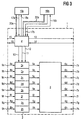
- the circuit cell 1 has a storage unit 2 for storage of data, a combinatorial circuit 3 for data processing and a memory control unit 4 for control the storage unit 2.
- the memory unit 2 contains a plurality of memory cells 2a, 2b, 2c, 2d, 2e, 2f, 2g, 2h for the temporary storage of data.
- the Storage unit 2 is preferably a BILBO register that is in different operating modes can be operated. It preferably points four operating modes, with the BILBO register in Normal operation as a register or buffer works, generated test patterns in a second operating mode and sends, receives test pattern data in a third operating mode and compressed and in a fourth mode of operation as serial Shift register is initialized by reading data or provides data for reading test data.
- the memory cells 2a-2h are each connected to the via internal data lines 5a-5h combinatorial circuit 3 connected.
- the combinatorial Circuit 3 performs data processing on the lines 5a-5h due data.
- the combinatorial circuit 3 is preferably a logic circuit made up of a plurality consists of gates.
- the combinatorial circuit 3 processes the data and outputs output data via lines 6a-6h on output data connections 7a-7h.
- the storage unit 2 is via internal data lines 8a-8h with data input connections 9a-9h connected.
- the one shown in Fig. 3 Embodiment corresponds to the number of output data connections 7a-7h of a circuit cell 1 according to the invention Number of input connections 9a-9h of the invention Circuit cell 1. This facilitates systolic construction with further circuit cells 1.
- the circuit cells 1 can in such a way in an overall circuit are distributed that between a transmission circuit cell and any number of a receiving circuit cell Data registers is provided.
- the storage unit 2 is connected via control lines 10, 11 the memory control unit 4 controls and receives in test mode a clock signal via a synchronization line 12. about the control lines 10, 11 becomes the operating mode of the storage unit 2 set.
- Via the control line 10 is a Command for generating the test pattern TMG and via the control line 11, a test pattern compression command TMK is sent.
- the four operating modes of the BILBO register 2 are set according to the following table. Operating mode TMK TMG Normal operation 0 0 Test pattern compression 1 0 Test pattern generation (shift register operation) 0 1 initialization 1 1
- the memory control unit 4 transmits via the synchronization line 12 a synchronization signal S for synchronization of the Storage unit 2 as a function of communication signals, the memory control unit 4 with memory control units other circuit cells.
- the memory controller is via communication line pairs 13, 14; 15, 16 on Memory control units can be connected by other circuit cells.
- Each communication line pair has a data transmission request line 13 for sending a request signal or request signals and a data reception
- the memory control unit 4 receives when the circuit cell 1 is a test pattern receiving circuit cell is configured, via the data transmission request line 15 a request signal for data transmission from a test pattern transmission circuit cell and sends an acknowledgment signal via the data reception confirmation line 16 to this test pattern transmit circuit cell data transfer back.
- the memory control unit 4 is in test mode via a communication line pair 17a, 18a; 17b, 18b to external test machines 19a, 19b connectable.
- the memory control unit 4 via an initialization line 17a through the Automatic test machine 19a initializes and sends during the test process internal status data via a status reporting line 18a on the test machines 19a.
- the test machine 19a has Initialization module on.
- the test machine 19b evaluates as Evaluation unit the test results.
- the test machines 19a, 19b are each in test operation via data lines 20a, 20b connected to the memory control unit 4.
- synchronization line 12 That via the synchronization line 12 to the storage unit 2 for synchronization of the storage unit during the test process sent synchronization signal S is by the memory control unit 4 depending on the communication signal lines 13, 14 and 15, 16 of further circuit cells exchanged communication signals formed.
- the synchronization signal S is not in the test machines 19a, 19b generated, but independently decentrally in the memory control unit 4 of the circuit cell 1.
- FIG. 4 shows a flow chart of the method according to the invention for testing circuit cells with integrated self-test function.
- step S1 the test machine 19a initializes a first one Standard cell 1 as a test pattern transmitter circuit cell and one second standard cell 1 as a test pattern receiving circuit cell.
- the associated Memory control units 4 initialized.
- Step S1 determines the number of test pattern loops N. The initialization takes place via a serial test path or resetting the registers.
- step S2 the local memory control unit 4 outputs the Transmitter circuit cell of the associated memory unit 2 the control lines issue a command to generate a test pattern.
- step S3 the storage unit 2 sets the generated test pattern via lines 5a-5h to the combinatorial circuit 3 for data processing.
- the combinatorial circuit 3 performs the test data processing and transfers the output lines 6a-6h a processed test data pattern to the downstream receiving circuit cell 1.
- step S4 the memory control unit 4 transmits the transmitter circuit cell a prompt signal over the communication line 13 to a memory control unit 4 of the downstream Receiving circuit cell.
- the memory control unit 4 After the memory control unit 4 receives the prompt signal or receive signal from the transmitter circuit cell in step S5, it gives the associated storage unit 2 a command for test pattern compression via the control lines.
- step S6 the memory controller sends the receiving circuit cell a confirmation signal or acknowledgment signal to the transmitter circuit cell.
- step S7 a counter n is incremented or checked whether that End of test pattern generation is reached.
- step S8 it is checked whether the number N of the set Test pattern loops is reached. If determined in step S8 will have to go through more test loops the flow returns to step S2.
- step S9 in which the memory control unit 4 of the receiving circuit cell the associated memory unit 2 in the test data evaluation mode switches.
- the memory control unit 4 sends the receiving circuit cell in step S10 a request signal to the Automatic test machines 19b for reading out on the associated memory unit 2 compressed test data.
- the read test data are then provided with a test data target response compared and determined whether the circuit cells the integrated circuit under test is faulty are or not.
- test pattern transmit circuit cell The synchronization between the test pattern transmit circuit cell and the test pattern receiving circuit cell, test pattern generation and / or Test pattern evaluation takes place in the case of the invention shown in FIG. 4 Process decentrally through that in the circuit cells included memory control units 4.
- the test machine 19a only provides initialization commands and no synchronization signals to the memory control units 4.
- Inverter chains to compensate for runtime differences even synchronization of the on the integrated circuit existing circuit cells are in the invention Test procedure not necessary. This will make the global Synchronization network of the integrated to be tested Circuit no longer needed and its power consumption is considerable reduced.
- the power supply lines and ground lines of the integrated circuit considerably be reduced because the different circuit units of the circuit cells at different times switch. This also increases the complexity of the integrated Circuit significantly reduced overall.
- the invention Test procedure also enables performance or performance of the integrated circuit reliably to determine.
- test method adapts when cooling the Switch to the speed increases.
- the test modules with local memory control unit 4 can also by Test procedures are tested using a global controller be synchronized.
- a test machine generates the necessary test response that the test transmission circuit cell from the Test receive circuit cell expected.
Landscapes
- Engineering & Computer Science (AREA)
- General Engineering & Computer Science (AREA)
- Physics & Mathematics (AREA)
- General Physics & Mathematics (AREA)
- Theoretical Computer Science (AREA)
- Computer Hardware Design (AREA)
- Quality & Reliability (AREA)
- Tests Of Electronic Circuits (AREA)
Abstract
Description

Senden eines Befehlssignals von der Speichersteuereinheit der Testmuster-Sendeschaltungszelle zu der zugehörigen Speichereinheit zum Generieren eines Testmuster,
Senden des generierten Testmusters von der Speichereinheit der Testmuster-Sendeschaltungszelle an die kombinatorische Schaltung zur Datenverarbeitung,
Senden eines Aufforderungssignals von der Speichersteuereinheit der Testmuster-Sendeschaltungszelle an die Speichersteuereinheit der Testmuster-Empfangsschaltungszelle,
Senden eines Befehls von der Speichersteuereinheit der Testmuster-Empfangsschaltungszelle an die zugehörige Speichereinheit zur Testmusterkomprimierung,
Senden eines Bestätigungssignals von der Speichersteuereinheit der Testmuster-Empfangsschaltungszelle an die Speichersteuereinheit der Testmuster-Sendeschaltungszelle,
Schalten der Speichereinheit der Testmuster-Empfangsschaltungszelle in den Testdaten-Auswertebetrieb durch die Speichersteuereinheit der Testmuster-Empfangsschaltungszelle,
Senden eines Aufforderungssignals an den Testautomaten zum Auslesen der Testdaten durch die Speichersteuereinheit der Testmuster-Empfangsschaltungszelle,
Auslesen der Testdaten durch den Testautomaten aus der Speichereinheit der Testmuster-Empfangsschaltungszelle.
| Betriebsart | TMK | TMG |
| Normalbetrieb | 0 | 0 |
| Testmusterkomprimierung | 1 | 0 |
| Testmustergenerierung (Schieberegisterbetrieb) | 0 | 1 |
| Initialisierung | 1 | 1 |
- 1
- Schaltungszelle
- 2
- Speichereinheit
- 3
- kombinatorische Schaltung
- 4
- Speichersteuerungseinheit
- 5
- Datenleitungen
- 6
- Datenleitungen
- 7
- Datenausgangsanschlüsse
- 8
- Datenleitungen
- 9
- Dateneingangsanschlüsse
- 10
- Steuerleitung
- 11
- Steuerleitung
- 12
- Synchronisierleitung
- 13
- Anforderungsleitung
- 14
- Bestätigungsleitung
- 15
- Anforderungsleitung
- 16
- Bestätigungsleitung
- 17a, 18b
- Initialisierungsleitungen
- 18a, 17b
- Zustandsmeldeleitungen
- 19a, 19b
- Testautomaten
- 20a, 20b
- Datenleitungen
Claims (11)
- Verfahren zum Testen von Schaltungszellen(1) einer integrierten Schaltung, wobei eine Schaltungszelle (1) jeweils eine kombinatorische Schaltung (3) zur Datenverarbeitung, eine Speichereinheit (2) und eine Speichersteuereinheit (4) enthält, wobei die Synchronisation zwischen den Schaltungszellen (1), die Testmustergenerierung und die Testmusterauswertung dezentral durch die in den Schaltungszellen (1) enthaltenen Speichersteuerungseinheiten (4) erfolgt und das Verfahren die folgenden Schritte aufweist:(a) Initialisieren (S1) einer Schaltungszelle als Testmuster-Sendeschaltungszelle und einer Schaltungszelle als Testmuster-Empfangsschaltungszelle;(b) Senden (S2) eines Befehlssignals von der Speichersteuereinheit (4) der Testmuster-Sendeschaltungszelle an die zugehörige Speichereinheit (2) zum Generieren eines Testmusters;(c) Anlegen (S3) des generierten Testmusters an die kombinatorische Schaltung (3) zur Datenverarbeitung durch die Speichereinheit der Testmuster-Sendeschaltungszelle;(d) Senden (S4) eines Anforderungssignals (R) durch die Speichersteuereinheit (4) der Testmuster-Sendeschaltungszelle an die Speichersteuereinheit (4) der Testmuster-Empfangsschaltungszelle;(e) Senden (S5) eines Befehls zur Testmusterkomprimierung an die Speichereinheit (2) der Testmuster-Empfangsschaltungszelle durch die Speichersteuereinheit (4) der Empfangsschaltungszelle;(f) Senden (S6)eines Bestätigungssignals (A) von der Speichersteuereinheit (4) der Testmuster-Empfangsschaltungszelle an die Speichersteuereinheit der Testmuster-Sendeschaltungszelle;(g) Schalten der Speichereinheit (2) der Testmuster-Empfangsschaltungszelle in einen Testdaten-Auswertungsbetrieb durch die Speichersteuereinheit (4) der Testmuster-Empfangsschaltungszelle;(h) Senden (S10) eines Aufforderungssignals an den Testautomaten (19) zum Auslesen der komprimierten Testdaten durch die Speichersteuereinheit (4) der Testmuster-Empfangsschaltungszelle;(i) Auslesen der Testdaten aus der Speichereinheit (2) der Testmuster-Empfangsschaltungszelle durch den Testautomaten (19).
- Verfahren nach Anspruch 1,
dadurch gekennzeichnet,
daß die ausgelesenen Testdaten mit einer Testdaten-Sollantwort verglichen werden. - Verfahren nach einem der vorangehenden Ansprüche,
dadurch gekennzeichnet,
daß die Speichereinheit (2) der Schaltungszelle durch ein Synchronisiersignal synchronisiert wird, das durch die zugehörige Speichersteuereinheit (4) in Abhängigkeit von Kommunikationssignalen erzeugt wird, welche die Speichersteuereinheit (4) mit Speichersteuereinheiten von weiteren Standardzellen austauscht. - Verfahren nach einem der vorangehenden Ansprüche,
dadurch gekennzeichnet,
daß die Speichersteuereinheiten (4) der verschiedenen Schaltungszellen Datensende-Aufforderungssignale und Datenempfangs-Bestätigungssignale untereinander als Kommunikationssignale austauschen. - Verfahren nach einem der vorangehenden Ansprüche,
dadurch gekennzeichnet,
daß die dezentrale Synchronisation über Handshake-Signale erfolgt. - Schaltungszelle in einer integrierten Schaltung mit eingebauter Selbsttestfunktion für eine modular aufgebaute Schaltung mit:(a) einer Speichereinheit (2) zum Speichern von Daten;(b) einer kombinatorischen Schaltung (3) zur Datenverarbeitung;(c) einer Speichersteuereinheit (4) zur Steuerung der Speichereinheit (2),
wobei die Speichersteuereinheit (4) derart konfigurierbar ist, daß sie in einem Sendebetrieb die Speichereinheit (2) als Testmustergenerator und in einem Empfangsbetrieb als Testmuster-Komprimierungseinrichtung einstellt, und die Speichersteuereinheit (4) ein Synchronisiersignal zur Synchronisation der Speichereinheit (2) in Abhängigkeit von Kommunikationssignalen erzeugt, die die Speichersteuereinheit (4) mit Speichersteuereinheiten von weiteren Schaltungszellen der integrierten Schaltung austauscht. - Schaltungszelle nach Anspruch 6,
dadurch gekennzeichnet,
daß die Speichersteuereinheit (4) über mindestens zwei Kommunikationsleitungspaare (13, 14; 15, 16) an Speichersteuereinheiten von weiteren Schaltungszellen (1) anschließbar ist, wobei jedes Kommunikationsleitungspaar eine Datensende-Aufforderungsleitung (13, 15) und eine Datenempfangs-Bestätigungsleitung (14, 16) aufweist. - Schaltungszelle nach einem der vorangehenden Ansprüche,
dadurch gekennzeichnet,
daß die Speichersteuereinheit (4) über ein Kommunikationsleitungspaar (17, 18) an mindestens einen Testautomaten (19) anschließbar ist, wobei die Speichersteuereinheit (4) über eine Initialisierungsleitung (17) durch den Testautomaten (19) mit Hilfe von dezentralen Synchronisierungssignalen initialisierbar ist und die Speichersteuereinheit (4) über eine Zustandsmeldeleitung (18) interne Zustandsdaten an den Testautomaten (19) sendet. - Schaltungszelle nach einem der vorangehenden Ansprüche,
dadurch gekennzeichnet,
daß die Speichereinheit (2) ein Register ist, das zwischen den verschiedenen Betriebsarten schaltbar ist. - Schaltungszelle nach Anspruch 9,
dadurch gekennzeichnet,
daß das Register zwischen einem normalen Datenspeicherbetrieb, einem Betrieb als serielles Schieberegister, einem Testkomprimierungsbetrieb und einen Initialisierungsbetrieb umschaltbar ist. - Schaltungszelle nach Anspruch 6,
dadurch gekennzeichnet,
daß die kombinatorische Schaltung (3) aus Signalleitungen besteht.
Applications Claiming Priority (2)
| Application Number | Priority Date | Filing Date | Title |
|---|---|---|---|
| DE19948904A DE19948904C1 (de) | 1999-10-11 | 1999-10-11 | Schaltungszelle mit eingebauter Selbsttestfunktion und Verfahren zum Testen hierfür |
| DE19948904 | 1999-10-11 |
Publications (2)
| Publication Number | Publication Date |
|---|---|
| EP1099952A1 true EP1099952A1 (de) | 2001-05-16 |
| EP1099952B1 EP1099952B1 (de) | 2004-12-29 |
Family
ID=7925216
Family Applications (1)
| Application Number | Title | Priority Date | Filing Date |
|---|---|---|---|
| EP00121371A Expired - Lifetime EP1099952B1 (de) | 1999-10-11 | 2000-10-11 | Schaltungszelle mit eingebauter Selbsttestfunktion und Verfahren zum Testen hierfür |
Country Status (3)
| Country | Link |
|---|---|
| US (1) | US6662326B1 (de) |
| EP (1) | EP1099952B1 (de) |
| DE (1) | DE19948904C1 (de) |
Cited By (1)
| Publication number | Priority date | Publication date | Assignee | Title |
|---|---|---|---|---|
| CN105438105A (zh) * | 2014-09-19 | 2016-03-30 | 英飞凌科技股份有限公司 | 针对电池和测试电路的系统和方法 |
Families Citing this family (5)
| Publication number | Priority date | Publication date | Assignee | Title |
|---|---|---|---|---|
| DE19948902C1 (de) * | 1999-10-11 | 2001-07-12 | Infineon Technologies Ag | Schaltungszelle zur Testmuster-Generierung und Testmuster-Kompression |
| US6934900B1 (en) * | 2001-06-25 | 2005-08-23 | Global Unichip Corporation | Test pattern generator for SRAM and DRAM |
| CN1695067A (zh) * | 2001-12-17 | 2005-11-09 | 皇家飞利浦电子股份有限公司 | 梯度线圈装置 |
| US8612815B2 (en) * | 2011-12-16 | 2013-12-17 | International Business Machines Corporation | Asynchronous circuit with an at-speed built-in self-test (BIST) architecture |
| US10473717B2 (en) * | 2016-11-09 | 2019-11-12 | Texas Instruments Incorporated | Methods and apparatus for test insertion points |
Citations (1)
| Publication number | Priority date | Publication date | Assignee | Title |
|---|---|---|---|---|
| US5173904A (en) * | 1987-06-02 | 1992-12-22 | Texas Instruments Incorporated | Logic circuits systems, and methods having individually testable logic modules |
Family Cites Families (5)
| Publication number | Priority date | Publication date | Assignee | Title |
|---|---|---|---|---|
| GB8432533D0 (en) * | 1984-12-21 | 1985-02-06 | Plessey Co Plc | Integrated circuits |
| JPH0682325B2 (ja) * | 1990-05-29 | 1994-10-19 | 株式会社東芝 | 情報処理装置のテスト容易化回路 |
| JP3377225B2 (ja) * | 1992-04-07 | 2003-02-17 | 富士写真フイルム株式会社 | チェック回路を含む集積回路 |
| DE69502827T2 (de) * | 1995-08-10 | 1998-10-15 | Hewlett Packard Gmbh | Elektronischer Schaltungs- oder Kartenprüfer und Verfahren zur Prüfung einer elektronischen Vorrichtung |
| JPH10319095A (ja) * | 1997-05-22 | 1998-12-04 | Mitsubishi Electric Corp | 半導体テスト装置 |
-
1999
- 1999-10-11 DE DE19948904A patent/DE19948904C1/de not_active Expired - Fee Related
-
2000
- 2000-10-11 EP EP00121371A patent/EP1099952B1/de not_active Expired - Lifetime
- 2000-10-11 US US09/686,834 patent/US6662326B1/en not_active Expired - Lifetime
Patent Citations (1)
| Publication number | Priority date | Publication date | Assignee | Title |
|---|---|---|---|---|
| US5173904A (en) * | 1987-06-02 | 1992-12-22 | Texas Instruments Incorporated | Logic circuits systems, and methods having individually testable logic modules |
Cited By (3)
| Publication number | Priority date | Publication date | Assignee | Title |
|---|---|---|---|---|
| CN105438105A (zh) * | 2014-09-19 | 2016-03-30 | 英飞凌科技股份有限公司 | 针对电池和测试电路的系统和方法 |
| CN105438105B (zh) * | 2014-09-19 | 2018-03-30 | 英飞凌科技股份有限公司 | 针对电池和测试电路的系统和方法 |
| US9995793B2 (en) | 2014-09-19 | 2018-06-12 | Infineon Technologies Ag | System and method for a built-in-self-test of a battery |
Also Published As
| Publication number | Publication date |
|---|---|
| EP1099952B1 (de) | 2004-12-29 |
| US6662326B1 (en) | 2003-12-09 |
| DE19948904C1 (de) | 2001-07-05 |
Similar Documents
| Publication | Publication Date | Title |
|---|---|---|
| DE3709032C2 (de) | ||
| DE69107463T2 (de) | Integrierte Schaltung, System und Verfahren zur Fehlererzeugung. | |
| DE3130714C2 (de) | ||
| DE69713084T2 (de) | Verfahren und vorrichtung zur erzeugung einer programmierbaren verzögerung | |
| DE19815263C2 (de) | Vorrichtung zur fehlertoleranten Ausführung von Programmen | |
| DE102010012904B4 (de) | Systeme zum Durchführen eines Tests | |
| DE3606650A1 (de) | Hardware logik-simulator | |
| DE69314683T2 (de) | Verfahren und Gerät zum Prüfen von Ein-/Ausgabeverbindungen des Randsteckverbinders einer Schaltkreiskarte mit Boundary Scan | |
| DE69003891T2 (de) | Testvorrichtung für gedruckte Schaltungskarten und ihre Anwendung für das Testen von gedruckten Schaltungskarten, in Form einer Multiplex-Demultiplexeinrichtung für numerische Signale. | |
| DE69321663T2 (de) | Hierarchisches Verbindungsverfahren, -gerät und -protokoll | |
| DE60010614T2 (de) | On-line Prüfung des programmierbaren Verbindungsnetzwerks in einer feldprogrammierbaren Gatteranordnung | |
| EP3149710B1 (de) | Fahrzeugdiagnosevorrichtung und datenübertragungsvorrichtung | |
| DE2813418A1 (de) | Einrichtung in einer elektronischen datenverarbeitungsanlage zur meldung von fehler- und betriebszustaenden | |
| DE69028498T2 (de) | Datenübertragungssystem und -verfahren | |
| DE3751083T2 (de) | Schnittstelle für seriellen Bus, fähig für den Datentransfer in verschiedenen Formaten. | |
| DE69211862T2 (de) | Zellenvermittlungsmodul und -netz mit vereinfachtem Prüfverfahren | |
| EP1099952B1 (de) | Schaltungszelle mit eingebauter Selbsttestfunktion und Verfahren zum Testen hierfür | |
| DE2641700C2 (de) | ||
| DE69315364T2 (de) | Verfahren zum Testen einer integrierten Schaltung und eine integrierte Schaltung mit einer Vielzahl von Funktionskomponenten und Verbindungs- und Schalter-Testkomponenten in verbindenden Kanälen zwischen Funktionskomponenten | |
| EP0265837A2 (de) | Schaltungsanordnung, deren Verwendung und Prüfverfahren für ein Nachrichtennetzwerk | |
| DE69031676T2 (de) | Architektur des Abtastpfads eines Systems | |
| DE112008001143T5 (de) | Serialisierung von Daten in einer Multi-Chip-Busimplementierung | |
| DE69130079T2 (de) | Datenverarbeitungsvorrichtung mit Prüfschaltung | |
| DE60315922T2 (de) | Scan-Path-Flip-Flop-Schaltung für eine integrierte Speicherschaltung | |
| DE3838939C2 (de) |
Legal Events
| Date | Code | Title | Description |
|---|---|---|---|
| PUAI | Public reference made under article 153(3) epc to a published international application that has entered the european phase |
Free format text: ORIGINAL CODE: 0009012 |
|
| AK | Designated contracting states |
Kind code of ref document: A1 Designated state(s): FR GB |
|
| AX | Request for extension of the european patent |
Free format text: AL;LT;LV;MK;RO;SI |
|
| 17P | Request for examination filed |
Effective date: 20010712 |
|
| AKX | Designation fees paid |
Free format text: FR GB |
|
| REG | Reference to a national code |
Ref country code: DE Ref legal event code: 8566 |
|
| GRAP | Despatch of communication of intention to grant a patent |
Free format text: ORIGINAL CODE: EPIDOSNIGR1 |
|
| GRAS | Grant fee paid |
Free format text: ORIGINAL CODE: EPIDOSNIGR3 |
|
| GRAA | (expected) grant |
Free format text: ORIGINAL CODE: 0009210 |
|
| AK | Designated contracting states |
Kind code of ref document: B1 Designated state(s): FR GB |
|
| REG | Reference to a national code |
Ref country code: GB Ref legal event code: FG4D Free format text: NOT ENGLISH |
|
| GBT | Gb: translation of ep patent filed (gb section 77(6)(a)/1977) |
Effective date: 20050321 |
|
| PLBE | No opposition filed within time limit |
Free format text: ORIGINAL CODE: 0009261 |
|
| STAA | Information on the status of an ep patent application or granted ep patent |
Free format text: STATUS: NO OPPOSITION FILED WITHIN TIME LIMIT |
|
| 26N | No opposition filed |
Effective date: 20050930 |
|
| ET | Fr: translation filed | ||
| PGFP | Annual fee paid to national office [announced via postgrant information from national office to epo] |
Ref country code: GB Payment date: 20061023 Year of fee payment: 7 |
|
| GBPC | Gb: european patent ceased through non-payment of renewal fee |
Effective date: 20071011 |
|
| PG25 | Lapsed in a contracting state [announced via postgrant information from national office to epo] |
Ref country code: GB Free format text: LAPSE BECAUSE OF NON-PAYMENT OF DUE FEES Effective date: 20071011 |
|
| REG | Reference to a national code |
Ref country code: FR Ref legal event code: PLFP Year of fee payment: 16 |
|
| PGFP | Annual fee paid to national office [announced via postgrant information from national office to epo] |
Ref country code: FR Payment date: 20151023 Year of fee payment: 16 |
|
| REG | Reference to a national code |
Ref country code: FR Ref legal event code: ST Effective date: 20170630 |
|
| PG25 | Lapsed in a contracting state [announced via postgrant information from national office to epo] |
Ref country code: FR Free format text: LAPSE BECAUSE OF NON-PAYMENT OF DUE FEES Effective date: 20161102 |