EP1098385A2 - Dielectric filter, composite dielectric filter, dielectric duplexer, dielectric diplexer, and communication apparatus incorporating the same - Google Patents
Dielectric filter, composite dielectric filter, dielectric duplexer, dielectric diplexer, and communication apparatus incorporating the same Download PDFInfo
- Publication number
- EP1098385A2 EP1098385A2 EP00122899A EP00122899A EP1098385A2 EP 1098385 A2 EP1098385 A2 EP 1098385A2 EP 00122899 A EP00122899 A EP 00122899A EP 00122899 A EP00122899 A EP 00122899A EP 1098385 A2 EP1098385 A2 EP 1098385A2
- Authority
- EP
- European Patent Office
- Prior art keywords
- dielectric
- filter
- coupling
- filters
- resonators
- Prior art date
- Legal status (The legal status is an assumption and is not a legal conclusion. Google has not performed a legal analysis and makes no representation as to the accuracy of the status listed.)
- Granted
Links
Images


Classifications
-
- H—ELECTRICITY
- H01—ELECTRIC ELEMENTS
- H01P—WAVEGUIDES; RESONATORS, LINES, OR OTHER DEVICES OF THE WAVEGUIDE TYPE
- H01P1/00—Auxiliary devices
- H01P1/20—Frequency-selective devices, e.g. filters
-
- H—ELECTRICITY
- H01—ELECTRIC ELEMENTS
- H01P—WAVEGUIDES; RESONATORS, LINES, OR OTHER DEVICES OF THE WAVEGUIDE TYPE
- H01P1/00—Auxiliary devices
- H01P1/20—Frequency-selective devices, e.g. filters
- H01P1/207—Hollow waveguide filters
- H01P1/208—Cascaded cavities; Cascaded resonators inside a hollow waveguide structure
- H01P1/2084—Cascaded cavities; Cascaded resonators inside a hollow waveguide structure with dielectric resonators
- H01P1/2086—Cascaded cavities; Cascaded resonators inside a hollow waveguide structure with dielectric resonators multimode
Definitions
- the present invention relates to filters incorporating dielectric resonators, composite dielectric filters such as duplexers, and communication apparatuses incorporating the same.
- cellular base stations in mobile communication systems have used composite dielectric filters formed by a plurality of dielectric resonators, such as diplexers used for transmission and duplexers used for transmission and reception.
- Japanese Unexamined Patent Application Publication No. 10-75104 provides a dielectric filter formed by using a plurality of TM double-mode dielectric resonators.
- this dielectric filter the opening faces of the TM double-mode dielectric resonators are aligned flush with each other.
- a metal panel is disposed to cover the opening faces.
- coupling loops are formed for inputting/outputting signals and performing coupling between the resonators.
- a plurality of the dielectric filters are arranged in parallel to each other to form a composite dielectric filter.
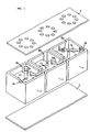
- Fig. 8 shows a structural example of the composite dielectric filter according to the conventional art.
- the reference numeral 9 denotes coaxial connectors for inputting the signals of three channels ch1, ch2, and ch3.
- the reference numeral 8 denotes a coaxial connector for power-synthesizing and outputting the three inputted signals.
- the reference characters R1a to R3c are TM double-mode dielectric resonators. These TM double-mode dielectric resonators serve as two-stage resonators by coupling between the resonance modes.
- coupling loops are used for performing the coupling between predetermined resonance modes of the adjacent dielectric resonators and performing the coupling between the predetermined resonance modes and the coaxial connectors.
- a coupling loop 3a couples to one of the resonance modes of each of the resonators R1a, R2a, and R3a.
- a coupling loop 3c couples to one of the resonance modes of each of the resonators R1c, R2c, and R3c.
- a coupling loop 3ab performs coupling between the predetermined resonance modes of the resonators R1a and R1b, coupling between the predetermined resonance modes of the resonators R2a and R2b, and coupling between the predetermined resonance modes of the resonators R3a and R3b.
- a coupling loop 3bc performs coupling between the predetermined resonance modes of the resonators R1b and R1c, coupling between the predetermined resonance modes of the resonators R2b and R2c, and coupling between the predetermined resonance modes of the resonators R3b and R3c.
- the above arrangement permits three dielectric filters F1, F2, and F3 to be constituted.
- a cutting jig is inserted through adjusting holes disposed in the metal panel, and a predetermined part of a dielectric core is cut off.
- a composite dielectric filter including a dielectric resonator formed by disposing a dielectric core in a cavity, a coupling loop for coupling to a predetermined resonance mode of the dielectric resonator, and a plurality of dielectric filters, each of the dielectric filters including the dielectric resonator and the coupling loop.
- the dielectric resonator and coupling loop of the dielectric filters are arranged in such a manner that the directions of the adjacent coupling loops between the dielectric filters are substantially vertical to each other.
- a dielectric filter including a plurality of dielectric resonators formed by disposing dielectric cores in cavities, and coupling loops for coupling to predetermined resonance modes of the dielectric resonators.
- the plurality of dielectric resonators is arranged in such a manner that a signal flowing from a signal input portion to a signal output portion is returned on its way, and, with the arrangement of the dielectric resonators, the coupling loops are arranged in such a manner that the directions of the adjacent coupling loops are substantially vertical to each other.
- a dielectric duplexer including the composite dielectric filter or two dielectric filters that are the same as the above dielectric filter, a first-filter input port used as a transmitted-signal input port, a second-filter output port used as a received-signal output port, and an input/output port common to the first filter and the second filter used as an antenna port.
- a dielectric diplexer including the composite dielectric filter or a plurality of dielectric filters that is the same as the above dielectric filter, used as a plurality of transmission filters passing signals transmitted from predetermined frequency channels, and an output port common to the transmission filters used as an antenna port.
- a communication apparatus including one of the composite dielectric filter, the dielectric filter, the dielectric duplexer, and the dielectric diplexer, which are described above.
- a dielectric diplexer according to a first embodiment of the present invention will be illustrated by referring to Figs. 1 to 4.
- Fig. 1 is an exploded perspective view showing the structure of one of a plurality of dielectric filters forming the dielectric diplexer.
- the reference numeral 1 denotes each rectangular-tube-shaped cavity whose upper and lower surfaces are open. Inside the cavity 1, a cross-shaped dielectric core 2 is integrally formed with the cavity 1. On the outer surface of each cavity 1, a conductor film of a silver electrode or the like is formed.
- the reference numeral 5 denotes a lower cavity cover for covering the lower surface of the cavity 1
- the reference numeral 6 denotes an upper cavity cover for covering the upper part of the cavity 1. Both covers are formed of metal plates.
- the reference characters Ra, Rb, and Rc denote dielectric resonators, each of which is formed by a cavity as a unit. As will be described below, each of the dielectric resonators Ra, Rb, and Rc forms a two-stage TM mode dielectric resonator.
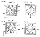
- Figs. 4A to 4D show examples of the electromagnetic distributions of the resonance modes of the dielectric resonator.
- a solid-line arrow represents an electric-field vector
- a broken-line arrow represents a magnetic-field vector.
- Each of Figs. 4A and 4B shows a fundamental mode used as a resonator. Since the mode shown in Fig. 4A is a mode whose electric field orients to a x + y direction, this mode is referred to as a TM 110 x+y mode. Similarly, since the mode shown in Fig. 4B is a mode whose electric field orients to a x - y direction, this mode is referred to as a TM 110 x-y mode.
- Figs. 4C and 4D show coupling modes obtained when the above two modes are fundamental modes. Fig. 4C shows an odd mode, and Fig. 4D shows an even mode.
- the resonance frequency of the TM 110 x+y mode can be adjusted.
- the resonance frequency of the TM 110 x+y mode can be adjusted.
- the sizes of holes hy1 and hy2 disposed in the axial directions of two dielectric pillars the frequencies of odd modes can be changed.
- the even-mode resonance frequencies can be changed.
- the resonance frequency of each stage and the coupling coefficient between the doubled resonators can be adjusted.
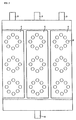
- Fig. 2 shows the top view of a dielectric diplexer formed by disposing three dielectric filters that are the same as the dielectric filter shown in Fig. 1, in which the upper cavity cover of the dielectric diplexer is removed.
- Fig. 3 shows the top view of the dielectric diplexer, in which the upper cavity cover thereof is disposed.
- the reference numeral 9 denotes coaxial connectors for inputting signals transmitted from three transmission channels ch1, ch2, and ch3, and the reference numerals 8 denotes a coaxial connector for outputting signals obtained by power-synthesizing the transmitted signals to an antenna.
- the reference number 7 denotes a power synthesizer for power-synthesizing the signals transmitted from three transmission filters.
- a dielectric filter F1 constituted of three dielectric resonators R1a, R1b, and R1c serves as a transmission filter for the channel ch1.
- a dielectric filter F2 constituted of three dielectric resonators R2a, R2b, and R2c serves as a transmission filter for the channel ch2.
- a dielectric filter F3 constituted of three dielectric resonators R3a, R3b, and R3c serves as a transmission filter for the channel ch3.
- the reference numeral 3a denotes a coupling loop connected to a central conductor of the coaxial connector 9
- the reference numeral 3c denotes a coupling loop connected to the power synthesizer 7.
- the reference numerals 3ab and 3bc denote coupling loops coupling to predetermined resonance modes of the adjacent dielectric resonators.
- the coupling loop 3a of the dielectric filter F1 performs magnetic-field coupling to the TM 110 x+y mode of the dielectric resonator R1a.
- the coupling loop 3c of the dielectric filter F1 performs magnetic-field coupling to the TM 110 x+y mode of the dielectric resonator R1c.
- the coupling loop 3ab of the dielectric filter F1 performs magnetic-field coupling to the TM 110 x+y mode of the dielectric resonator R1a, and, at the same time, performs magnetic-field coupling to the TM 110 x+y mode of the dielectric resonator R1b.
- the coupling loop 3bc of the dielectric filter F1 performs magnetic-field coupling to the TM 110 x+y mode of the dielectric resonator R1b, and, at the same time, performs magnetic-field coupling to the TM 110 x+y mode of the dielectric resonator R1c.
- the dielectric filter F1 serves as a filter having band pass characteristics constituted of a six-stage resonator.
- the dielectric filters F2 and F3 serve as filters having band pass characteristics constituted of a six-stage resonator, respectively.
- coupling loops are disposed in such a manner that the directions of the adjacent coupling loops are substantially vertical to each other.
- predetermined parts of the dielectric cores inside the cavities are cut off via adjusting holes H disposed in the upper cavity cover 6.
- the adjacent coupling loops of the adjacent dielectric filters hardly perform magnetic-field coupling therebetween, since the directions of the coupling loops are vertical to each other.
- leakage and interference of signals hardly occur. That is, in Fig. 2, for example, since the coupling loops 3a of the dielectric filters F1 and F2 do not perform magnetic-field coupling at the parts, since the directions of the loops are vertical to each other.
- the coupling loops 3c of the dielectric filters F1 and F2 do not perform magnetic-field coupling at the parts, since the directions of the loops are vertical to each other.
- the coupling loops 3ab of the dielectric filters F1 and F2 since the directions of the adjacent loops are vertical to each other, the coupling loops 3ab and the coupling loops 3bc, respectively, do not perform magnetic-field coupling. These relationships also apply to cases between the dielectric filters F2 and F3. As a result, even when the dielectric filters are close to each other and the characteristics-adjusting holes in the cavity cover are open, the coupling loops of the mutually adjacent dielectric filters hardly perform magnetic-field coupling. Thus, leakage and interference of signals hardly occur.
- d dielectric duplexer according to a second embodiment of the present invention.
- Fig. 5 shows a top view of the dielectric duplexer, in which the upper cavity cover of the dielectric duplexer is removed.
- the reference numeral 10 denotes a coaxial connector for inputting a transmitted signal Tx, and the coaxial connector 10 is connected from a transmitter.
- the reference numeral 12 denotes a coaxial connector for outputting a received signal, and the coaxial connector 12 is connected to a reception circuit.
- the reference numeral 11 denotes a coaxial connector for outputting a transmitted signal and inputting a received signal, and the coaxial connector 11 is connected to an antenna.
- a part indicated by the reference numeral 15 constitutes a branching unit for branching transmitted/received signals.
- a dielectric filter Ft constituted of three dielectric resonators Rta, Rtb, and Rtc serves as a transmission filter.
- a dielectric filter Fr constituted of three dielectric resonators Rra, Rrb, and Rrc serves as a reception filter.
- the reference numeral 3a denotes a coupling loop connected to a central conductor of the coaxial connector 10
- the reference numeral 3c denotes a coupling loop connected to the branching unit 15.
- the reference numerals 3ab and 3bc denote coupling loops for coupling to predetermined resonance modes of the adjacent dielectric resonators.
- the coupling loop 3a of the dielectric filter Ft performs magnetic-field coupling to the TM 110 x+y mode of the dielectric resonator Rta.
- the coupling loop 3c of the dielectric filter Ft performs magnetic-field coupling to the TM 110 x+y mode of the dielectric resonator Rtc.
- the coupling loop 3ab of the dielectric filter Ft performs magnetic-field coupling to the TM 110 x+y mode of the dielectric resonator Rta, and at the same time, performs magnetic-field coupling to the TM 110 x+y mode of the dielectric resonator Rtb.
- the coupling loop 3bc of the dielectric filter Ft performs magnetic-field coupling to the TM 110 x+y mode of the dielectric resonator Rtb, and at the same time, performs magnetic-field coupling to the TM 110 x+y mode of the dielectric resonator Rtc.
- the dielectric filter Ft serves as a filter having band pass characteristics constituted of a six-stage resonator.
- the dielectric filter Fr serves as a filter having band pass characteristics formed of a six-stage resonator.
- coupling loops are disposed in such a manner that the directions of the adjacent coupling loops are substantially vertical to each other.
- predetermined parts of the dielectric cores inside the cavities are cut off via the adjusting holes H disposed in the upper cavity cover.
- the adjacent coupling loops hardly perform magnetic-field coupling therebetween, since the directions of the loops are vertical to each other. Thus, leakage and interference of signals hardly occur.
- the magnetic-fields of both loops leaking from the adjusting holes perform coupling therebetween.
- the resonator of TM 110 x+y mode as the resonance mode of the dielectric resonator Rrc coupling to the coupling loop 3bc is not the last-stage resonator of the reception filter.
- the TM 110 x+y mode resonator coupling to the coupling loop 3c of the dielectric filter Fr is the last-stage resonator.
- Fig. 6 shows the top view of the dielectric filter in which the upper cavity cover of the filter is removed.
- the reference numeral 13 denotes a signal input coaxial connector
- the reference numeral 14 denotes a signal output coaxial connector.
- the reference characters Ra, Rb, Rc, and Rd denote TM double-mode dielectric resonators.
- the structures of these dielectric resonators are the same as those of the dielectric resonators used in the first and second embodiments.
- the reference numeral 3a denotes a coupling loop connected to a central conductor of the coaxial connector 13.
- the reference numeral 3d denotes a coupling loop connected to a central conductor of the coaxial connector 14.
- the reference characters 3ab, 3bc, and 3cd denote coupling loops for coupling to predetermined resonance modes of the adjacent dielectric resonators.
- the coupling loop 3a performs magnetic-field coupling to the TM 110 x+y mode of the dielectric resonator Ra.
- the coupling loop 3d performs magnetic-field coupling to the TM 110 x+y mode of the dielectric resonator Rd.
- the coupling loop 3ab performs magnetic-field coupling to the TM 110 x+y mode of the dielectric resonator Ra, and at the same time, performs magnetic-field coupling to the TM 110 x+y mode of the dielectric resonator Rb.
- the coupling loop 3bc performs magnetic-field coupling to the TM 110 x+y mode of the dielectric resonator Rb, and at the same time, performs magnetic-field coupling to the TM 110 x+y mode of the dielectric resonator Rc.
- the coupling loop 3cd performs mantic-field coupling to the TM 110 x+y mode of the dielectric resonator Rc, and, at the same time, performs magnetic-field coupling to the TM 110 x+y mode of the dielectric resonator Rd.
- the dielectric filter serves as a filter having band pass characteristics constituted of an eight-stage resonator.
- the adjacent coupling loops hardly perform magnetic-field coupling therebetween, since the directions of the loops are vertical to each other. Thus, leakage and interference of signals hardly occur.
- Fig. 7 shows a communication apparatus used in a base station in a cellular-type mobile communication system.
- a diplexer shown in Fig. 7 is equivalent to the dielectric diplexer shown in the first embodiment.
- the dielectric duplexer shown in the second embodiment is used.
- the dielectric filter shown in the third embodiment is used.
- the diplexer power-synthesizes transmitted signals Tx1, Tx2, and Tx3 of three channels output from the transmission circuit to supply to a transmitted signal input port of the duplexer.
- the duplexer outputs the transmitted signal to the antenna, and then supplies the signal received from the antenna to the reception filter.
- the reception filter supplies a signal Rx of a reception frequency band to the reception circuit.
- the coupling loops of the mutually adjacent dielectric filters hardly couple to each other.
- the isolation between the adjacent dielectric filters can be obtained. As a result, deterioration of filter characteristics can be prevented.
- the third aspect of the invention when the first filter as a transmission filter and the second filter as a reception filter are close to each other, since the isolation between both filters can be obtained, the entire size of the dielectric duplexer can be reduced.
- the fourth aspect of the invention when the signals of the plurality of channels are dealt with, even when the filters are disposed closely to each other, since the isolation therebetween can be secured, the entire size of the dielectric diplexer can be reduced.
- the entire size of the communication apparatus can be reduced.
Landscapes
- Control Of Motors That Do Not Use Commutators (AREA)
Abstract
Description
- The present invention relates to filters incorporating dielectric resonators, composite dielectric filters such as duplexers, and communication apparatuses incorporating the same.
- Conventionally, for example, cellular base stations in mobile communication systems have used composite dielectric filters formed by a plurality of dielectric resonators, such as diplexers used for transmission and duplexers used for transmission and reception.
- For example, Japanese Unexamined Patent Application Publication No. 10-75104 provides a dielectric filter formed by using a plurality of TM double-mode dielectric resonators. In this dielectric filter, the opening faces of the TM double-mode dielectric resonators are aligned flush with each other. A metal panel is disposed to cover the opening faces. In the panel, coupling loops are formed for inputting/outputting signals and performing coupling between the resonators. A plurality of the dielectric filters are arranged in parallel to each other to form a composite dielectric filter.
- Fig. 8 shows a structural example of the composite dielectric filter according to the conventional art. In Fig. 8, the
reference numeral 9 denotes coaxial connectors for inputting the signals of three channels ch1, ch2, and ch3. Thereference numeral 8 denotes a coaxial connector for power-synthesizing and outputting the three inputted signals. The reference characters R1a to R3c are TM double-mode dielectric resonators. These TM double-mode dielectric resonators serve as two-stage resonators by coupling between the resonance modes. In addition, coupling loops are used for performing the coupling between predetermined resonance modes of the adjacent dielectric resonators and performing the coupling between the predetermined resonance modes and the coaxial connectors. Specifically, acoupling loop 3a couples to one of the resonance modes of each of the resonators R1a, R2a, and R3a. Acoupling loop 3c couples to one of the resonance modes of each of the resonators R1c, R2c, and R3c. In addition, a coupling loop 3ab performs coupling between the predetermined resonance modes of the resonators R1a and R1b, coupling between the predetermined resonance modes of the resonators R2a and R2b, and coupling between the predetermined resonance modes of the resonators R3a and R3b. Similarly, a coupling loop 3bc performs coupling between the predetermined resonance modes of the resonators R1b and R1c, coupling between the predetermined resonance modes of the resonators R2b and R2c, and coupling between the predetermined resonance modes of the resonators R3b and R3c. The above arrangement permits three dielectric filters F1, F2, and F3 to be constituted. - When the characteristics of the dielectric filter are adjusted, a cutting jig is inserted through adjusting holes disposed in the metal panel, and a predetermined part of a dielectric core is cut off.
- However, in the composite dielectric filter according to the conventional art as shown in Fig. 8, when the plurality of dielectric filters is arranged close to each other, the electric-fields of the coupling loops leaking from the adjusting holes are likely to easily couple to each other, whereby isolation between the adjacent filters is reduced, with the result that attenuation characteristics are deteriorated.
- Accordingly, it is an object of the present invention to provide a dielectric filter, a composite dielectric filter, a dielectric duplexer, and a dielectric diplexer, in which isolation between adjacent filters can be obtained, and deterioration of filter characteristics can thereby be prevented. It is another object of the present invention to provide a communication apparatus incorporating one of the dielectric filter, the composite dielectric filter, the dielectric duplexer, and the dielectric diplexer.
- According to a first aspect of the present invention, there is provided a composite dielectric filter including a dielectric resonator formed by disposing a dielectric core in a cavity, a coupling loop for coupling to a predetermined resonance mode of the dielectric resonator, and a plurality of dielectric filters, each of the dielectric filters including the dielectric resonator and the coupling loop. In the above composite dielectric filter, the dielectric resonator and coupling loop of the dielectric filters are arranged in such a manner that the directions of the adjacent coupling loops between the dielectric filters are substantially vertical to each other.
- With this structure, even when the dielectric filters are close to each other, the adjacent coupling loops between the dielectric filters hardly couple to each other.
- According to a second aspect of the present invention, there is provided a dielectric filter including a plurality of dielectric resonators formed by disposing dielectric cores in cavities, and coupling loops for coupling to predetermined resonance modes of the dielectric resonators. In this dielectric filter, the plurality of dielectric resonators is arranged in such a manner that a signal flowing from a signal input portion to a signal output portion is returned on its way, and, with the arrangement of the dielectric resonators, the coupling loops are arranged in such a manner that the directions of the adjacent coupling loops are substantially vertical to each other.
- With this arrangement, even in places where the dielectric resonators are adjacent to each other in the arrangement of the dielectric resonators, the coupling loops of the adjacent dielectric resonators hardly couple to each other.
- According to a third aspect of the present invention, there is provided a dielectric duplexer including the composite dielectric filter or two dielectric filters that are the same as the above dielectric filter, a first-filter input port used as a transmitted-signal input port, a second-filter output port used as a received-signal output port, and an input/output port common to the first filter and the second filter used as an antenna port.
- According to a fourth aspect of the present invention, there is provided a dielectric diplexer including the composite dielectric filter or a plurality of dielectric filters that is the same as the above dielectric filter, used as a plurality of transmission filters passing signals transmitted from predetermined frequency channels, and an output port common to the transmission filters used as an antenna port.
- According to a fifth aspect of the present invention, there is provided a communication apparatus including one of the composite dielectric filter, the dielectric filter, the dielectric duplexer, and the dielectric diplexer, which are described above.
-
- Fig. 1 is an exploded perspective view showing the structure of a dielectric filter of a dielectric diplexer according to a first embodiment of the present invention;
- Fig. 2 is a top view of the dielectric diplexer in which the upper cavity cover of the diplexer is removed;
- Fig. 3 is a top view of the dielectric diplexer in which the upper cavity cover of the diplexer is disposed;
- Figs. 4A, 4B, 4C, and 4D show examples of the electric-field distributions of the resonance modes of the dielectric resonator used in the dielectric diplexer;
- Fig. 5 shows the structure of a dielectric duplexer according to a second embodiment of the present invention;
- Fig. 6 shows the structure of a dielectric filter according to a third embodiment of the present invention;
- Fig. 7 shows the structure of a communication apparatus according to a fourth embodiment of the present invention; and
- Fig. 8 shows a view of the structural example of a composite dielectric filter according to a conventional art.
-
- The structure of a dielectric diplexer according to a first embodiment of the present invention will be illustrated by referring to Figs. 1 to 4.
- Fig. 1 is an exploded perspective view showing the structure of one of a plurality of dielectric filters forming the dielectric diplexer. In Fig. 1, the reference numeral 1 denotes each rectangular-tube-shaped cavity whose upper and lower surfaces are open. Inside the cavity 1, a cross-shaped
dielectric core 2 is integrally formed with the cavity 1. On the outer surface of each cavity 1, a conductor film of a silver electrode or the like is formed. Thereference numeral 5 denotes a lower cavity cover for covering the lower surface of the cavity 1, and thereference numeral 6 denotes an upper cavity cover for covering the upper part of the cavity 1. Both covers are formed of metal plates. - The reference characters Ra, Rb, and Rc denote dielectric resonators, each of which is formed by a cavity as a unit. As will be described below, each of the dielectric resonators Ra, Rb, and Rc forms a two-stage TM mode dielectric resonator.
- Figs. 4A to 4D show examples of the electromagnetic distributions of the resonance modes of the dielectric resonator. In these figures, a solid-line arrow represents an electric-field vector, and a broken-line arrow represents a magnetic-field vector. Each of Figs. 4A and 4B shows a fundamental mode used as a resonator. Since the mode shown in Fig. 4A is a mode whose electric field orients to a x + y direction, this mode is referred to as a TM110 x+y mode. Similarly, since the mode shown in Fig. 4B is a mode whose electric field orients to a x - y direction, this mode is referred to as a TM110 x-y mode. In addition, Figs. 4C and 4D show coupling modes obtained when the above two modes are fundamental modes. Fig. 4C shows an odd mode, and Fig. 4D shows an even mode.
- With the above relationship, of holes ha1, ha2, hb1, and hb2 disposed at corners of the cross-shaped
dielectric core 2, by the sizes of the holes hb1 and hb2, the resonance frequency of the TM110 x+y mode can be adjusted. Similarly, by the sizes of the holes ha1 and ha2, the resonance frequency of the TM110 x+y mode can be adjusted. In addition, by the sizes of holes hy1 and hy2 disposed in the axial directions of two dielectric pillars, the frequencies of odd modes can be changed. By changing the sizes of holes hx1 and hx2, the even-mode resonance frequencies can be changed. With this arrangement, the coupling strength between the TM110 x+y mode and the TM110 x+y mode can be adjusted. - By cutting a predetermined hole of the dielectric core via the holes disposed in the
upper cavity cover 6 shown in Fig. 1, the resonance frequency of each stage and the coupling coefficient between the doubled resonators can be adjusted. - Fig. 2 shows the top view of a dielectric diplexer formed by disposing three dielectric filters that are the same as the dielectric filter shown in Fig. 1, in which the upper cavity cover of the dielectric diplexer is removed. Fig. 3 shows the top view of the dielectric diplexer, in which the upper cavity cover thereof is disposed.
- In each of Figs. 2 and 3, the
reference numeral 9 denotes coaxial connectors for inputting signals transmitted from three transmission channels ch1, ch2, and ch3, and thereference numerals 8 denotes a coaxial connector for outputting signals obtained by power-synthesizing the transmitted signals to an antenna. The reference number 7 denotes a power synthesizer for power-synthesizing the signals transmitted from three transmission filters. A dielectric filter F1 constituted of three dielectric resonators R1a, R1b, and R1c serves as a transmission filter for the channel ch1. Similarly, a dielectric filter F2 constituted of three dielectric resonators R2a, R2b, and R2c serves as a transmission filter for the channel ch2. A dielectric filter F3 constituted of three dielectric resonators R3a, R3b, and R3c serves as a transmission filter for the channel ch3. - In the three transmission filters, the
reference numeral 3a denotes a coupling loop connected to a central conductor of thecoaxial connector 9, and thereference numeral 3c denotes a coupling loop connected to the power synthesizer 7. In addition, the reference numerals 3ab and 3bc denote coupling loops coupling to predetermined resonance modes of the adjacent dielectric resonators. - With the above arrangement, the
coupling loop 3a of the dielectric filter F1 performs magnetic-field coupling to the TM110 x+y mode of the dielectric resonator R1a. Thecoupling loop 3c of the dielectric filter F1 performs magnetic-field coupling to the TM110 x+y mode of the dielectric resonator R1c. In addition, the coupling loop 3ab of the dielectric filter F1 performs magnetic-field coupling to the TM110 x+y mode of the dielectric resonator R1a, and, at the same time, performs magnetic-field coupling to the TM110 x+y mode of the dielectric resonator R1b. Furthermore, the coupling loop 3bc of the dielectric filter F1 performs magnetic-field coupling to the TM110 x+y mode of the dielectric resonator R1b, and, at the same time, performs magnetic-field coupling to the TM110 x+y mode of the dielectric resonator R1c. In this way, the dielectric filter F1 serves as a filter having band pass characteristics constituted of a six-stage resonator. - Similarly, the dielectric filters F2 and F3 serve as filters having band pass characteristics constituted of a six-stage resonator, respectively. In this case, between the dielectric filters F1 and F2, and between the dielectric filters F2 and F3, coupling loops are disposed in such a manner that the directions of the adjacent coupling loops are substantially vertical to each other.
- In order to adjust the characteristics of the dielectric filters, as shown in Fig. 3, predetermined parts of the dielectric cores inside the cavities are cut off via adjusting holes H disposed in the
upper cavity cover 6. - With the above arrangement, the adjacent coupling loops of the adjacent dielectric filters hardly perform magnetic-field coupling therebetween, since the directions of the coupling loops are vertical to each other. Thus, between the adjacent coupling loops, leakage and interference of signals hardly occur. That is, in Fig. 2, for example, since the
coupling loops 3a of the dielectric filters F1 and F2 do not perform magnetic-field coupling at the parts, since the directions of the loops are vertical to each other. In addition, since thecoupling loops 3c of the dielectric filters F1 and F2 do not perform magnetic-field coupling at the parts, since the directions of the loops are vertical to each other. Also, regarding the coupling loops 3ab of the dielectric filters F1 and F2, and regarding the coupling loops 3bc thereof, since the directions of the adjacent loops are vertical to each other, the coupling loops 3ab and the coupling loops 3bc, respectively, do not perform magnetic-field coupling. These relationships also apply to cases between the dielectric filters F2 and F3. As a result, even when the dielectric filters are close to each other and the characteristics-adjusting holes in the cavity cover are open, the coupling loops of the mutually adjacent dielectric filters hardly perform magnetic-field coupling. Thus, leakage and interference of signals hardly occur. - Next, referring to Fig. 5, a description will be given of d dielectric duplexer according to a second embodiment of the present invention.
- Fig. 5 shows a top view of the dielectric duplexer, in which the upper cavity cover of the dielectric duplexer is removed. In Fig. 5, the
reference numeral 10 denotes a coaxial connector for inputting a transmitted signal Tx, and thecoaxial connector 10 is connected from a transmitter. Thereference numeral 12 denotes a coaxial connector for outputting a received signal, and thecoaxial connector 12 is connected to a reception circuit. Thereference numeral 11 denotes a coaxial connector for outputting a transmitted signal and inputting a received signal, and thecoaxial connector 11 is connected to an antenna. A part indicated by thereference numeral 15 constitutes a branching unit for branching transmitted/received signals. A dielectric filter Ft constituted of three dielectric resonators Rta, Rtb, and Rtc serves as a transmission filter. A dielectric filter Fr constituted of three dielectric resonators Rra, Rrb, and Rrc serves as a reception filter. - In the dielectric filter Ft, the
reference numeral 3a denotes a coupling loop connected to a central conductor of thecoaxial connector 10, and thereference numeral 3c denotes a coupling loop connected to the branchingunit 15. In addition, the reference numerals 3ab and 3bc denote coupling loops for coupling to predetermined resonance modes of the adjacent dielectric resonators. - With the above arrangement, the
coupling loop 3a of the dielectric filter Ft performs magnetic-field coupling to the TM110 x+y mode of the dielectric resonator Rta. Thecoupling loop 3c of the dielectric filter Ft performs magnetic-field coupling to the TM110 x+y mode of the dielectric resonator Rtc. The coupling loop 3ab of the dielectric filter Ft performs magnetic-field coupling to the TM110 x+y mode of the dielectric resonator Rta, and at the same time, performs magnetic-field coupling to the TM110 x+y mode of the dielectric resonator Rtb. In addition, the coupling loop 3bc of the dielectric filter Ft performs magnetic-field coupling to the TM110 x+y mode of the dielectric resonator Rtb, and at the same time, performs magnetic-field coupling to the TM110 x+y mode of the dielectric resonator Rtc. In this way, the dielectric filter Ft serves as a filter having band pass characteristics constituted of a six-stage resonator. - Similarly, the dielectric filter Fr serves as a filter having band pass characteristics formed of a six-stage resonator. In this case, between the dielectric filters Ft and Fr, coupling loops are disposed in such a manner that the directions of the adjacent coupling loops are substantially vertical to each other.
- In order to adjust the characteristics of the dielectric filters, as in the case of the first embodiment, predetermined parts of the dielectric cores inside the cavities are cut off via the adjusting holes H disposed in the upper cavity cover.
- With the above arrangement, the adjacent coupling loops hardly perform magnetic-field coupling therebetween, since the directions of the loops are vertical to each other. Thus, leakage and interference of signals hardly occur.
- As indicated by a broken line L1 in Fig. 5, since the direction of the
coupling loop 3a of the dielectric filter Ft and the direction of a part of the coupling loop 3bc of the dielectric filter Fr are in a parallel relationship, the magnetic-fields of both loops leaking from the adjusting holes perform coupling therebetween. However, the resonator of TM110 x+y mode as the resonance mode of the dielectric resonator Rrc coupling to the coupling loop 3bc is not the last-stage resonator of the reception filter. The TM110 x+y mode resonator coupling to thecoupling loop 3c of the dielectric filter Fr is the last-stage resonator. Thus, with the last-stage resonator, a transmitted signal leaking from thecoupling loop 3a of the dielectric filter Ft to the coupling loop 3bc of the dielectric filter Fr is attenuated. As a result, the transmitted signal has no influence on the receiver. In addition, as indicated by a broken line L2 in Fig. 5, since the direction of thecoupling loop 3c of the dielectric filter Fr and the direction of a part of the coupling loop 3ab of the dielectric filter Ft are also parallel, the leaking waves of both loops perform magnetic-field coupling to each other. However, since the amount of coupling is very little, there is almost no influence on the reception circuit. - Next, referring to Fig. 6, a description will be given of the structural example of a dielectric filter according to a third embodiment of the present invention.
- Fig. 6 shows the top view of the dielectric filter in which the upper cavity cover of the filter is removed. In Fig. 6, the
reference numeral 13 denotes a signal input coaxial connector, and thereference numeral 14 denotes a signal output coaxial connector. The reference characters Ra, Rb, Rc, and Rd denote TM double-mode dielectric resonators. The structures of these dielectric resonators are the same as those of the dielectric resonators used in the first and second embodiments. - The
reference numeral 3a denotes a coupling loop connected to a central conductor of thecoaxial connector 13. The reference numeral 3d denotes a coupling loop connected to a central conductor of thecoaxial connector 14. In addition, the reference characters 3ab, 3bc, and 3cd denote coupling loops for coupling to predetermined resonance modes of the adjacent dielectric resonators. - The
coupling loop 3a performs magnetic-field coupling to the TM110 x+y mode of the dielectric resonator Ra. The coupling loop 3d performs magnetic-field coupling to the TM110 x+y mode of the dielectric resonator Rd. The coupling loop 3ab performs magnetic-field coupling to the TM110 x+y mode of the dielectric resonator Ra, and at the same time, performs magnetic-field coupling to the TM110 x+y mode of the dielectric resonator Rb. In addition, the coupling loop 3bc performs magnetic-field coupling to the TM110 x+y mode of the dielectric resonator Rb, and at the same time, performs magnetic-field coupling to the TM110 x+y mode of the dielectric resonator Rc. The coupling loop 3cd performs mantic-field coupling to the TM110 x+y mode of the dielectric resonator Rc, and, at the same time, performs magnetic-field coupling to the TM110 x+y mode of the dielectric resonator Rd. In this way, the dielectric filter serves as a filter having band pass characteristics constituted of an eight-stage resonator. - With the above arrangement, the adjacent coupling loops hardly perform magnetic-field coupling therebetween, since the directions of the loops are vertical to each other. Thus, leakage and interference of signals hardly occur.
- Next, referring to Fig. 7, a description will be given of the structural example of a communication apparatus according to the present invention.
- Fig. 7 shows a communication apparatus used in a base station in a cellular-type mobile communication system. A diplexer shown in Fig. 7 is equivalent to the dielectric diplexer shown in the first embodiment. As a duplexer, the dielectric duplexer shown in the second embodiment is used. Furthermore, as a reception filter, the dielectric filter shown in the third embodiment is used. The diplexer power-synthesizes transmitted signals Tx1, Tx2, and Tx3 of three channels output from the transmission circuit to supply to a transmitted signal input port of the duplexer. The duplexer outputs the transmitted signal to the antenna, and then supplies the signal received from the antenna to the reception filter. The reception filter supplies a signal Rx of a reception frequency band to the reception circuit.
- As described above, according to the first and second aspects of the invention, even when the dielectric filters are close to each other, the coupling loops of the mutually adjacent dielectric filters hardly couple to each other. Thus, while reducing the size of the entire structure of the dielectric filter, the isolation between the adjacent dielectric filters can be obtained. As a result, deterioration of filter characteristics can be prevented.
- According to the third aspect of the invention, when the first filter as a transmission filter and the second filter as a reception filter are close to each other, since the isolation between both filters can be obtained, the entire size of the dielectric duplexer can be reduced.
- According to the fourth aspect of the invention, when the signals of the plurality of channels are dealt with, even when the filters are disposed closely to each other, since the isolation therebetween can be secured, the entire size of the dielectric diplexer can be reduced.
- According to the fifth aspect of the invention, since a compact dielectric filter and a compact composite dielectric filter having predetermined filter characteristics are used, the entire size of the communication apparatus can be reduced.
- While the preferred embodiments of the present invention have been described above, it is to be understood that various modifications and changes will be made without departing the scope and spirit of the invention.
Claims (5)
- A composite dielectric filter comprising:a dielectric resonator (Ra, Rb, Rc) formed by disposing a dielectric core (2) in a cavity (1);a coupling loop (3a, 3c, 3ab, 3bc) for coupling to a predetermined resonance mode of the dielectric resonator; anda plurality of dielectric filters (F1, F2, F3), each of the dielectric filters including the dielectric resonator (Ra, Rb, Rc) and the coupling loop (3a, 3c, 3ab, 3bc);
wherein the dielectric resonator (Ra, Rb, Rc) and the coupling loop (3a, 3c, 3ab, 3bc) included in each of the dielectric filters (F1, F2, F3) are arranged in such a manner that the directions of adjacent coupling loops between the dielectric filters (F1, F2, F3) are substantially vertical to each other. - A dielectric filter comprising:a plurality of dielectric resonators (Ra, Rb, Rc; Ra, Rb, Rc, Rd) formed by disposing dielectric cores in cavities; andcoupling loops (3a, 3c, 3ab, 3bc; 3a, 3d, 3ab, 3bc, 3cd) for coupling to predetermined resonance modes of the dielectric resonators (Ra, Rb, Rc; Ra, Rb, Rc, Rd);
wherein the plurality of dielectric resonators (Ra, Rb, Rc; Ra, Rb, Rc, Rd) is arranged in such a manner that a signal flowing from a signal input portion (13) to a signal output portion (14) is returned on its way, and, with the arrangement of the dielectric resonators (Ra, Rb, Rc; Ra, Rb, Rc, Rd), the coupling loops (3a, 3c, 3ab, 3bc; 3a, 3d, 3ab, 3bc, 3cd) are arranged in such a manner that the directions of the adjacent coupling loops (3a, 3c, 3ab, 3bc; 3a, 3d, 3ab, 3bc, 3cd) are substantially vertical to each other. - A dielectric duplexer comprising:the composite dielectric filter according to Claim 1 or two dielectric filters that are the same as the dielectric filter according to Claim 2;a first-filter input port (10) used as a transmitted-signal input port;a second-filter output port (12) used as a received-signal output port; andan input/output port (11) common to the first filter and the second filter used as an antenna port.
- A dielectric diplexer comprising:the composite dielectric filter according to Claim 1 or a plurality of dielectric filters that is the same as the dielectric filter according to Claim 2, used as a plurality of transmission filters passing signals transmitted from predetermined frequency channels (9); andan output port (8) common to the transmission filters, which is used as an antenna port.
- A communication apparatus comprising one of the composite dielectric filter according to Claim 1, the dielectric filter according to Claim 2, the dielectric duplexer according to Claim 3, and the dielectric diplexer according to Claim 4.
Applications Claiming Priority (2)
| Application Number | Priority Date | Filing Date | Title |
|---|---|---|---|
| JP31309799 | 1999-11-02 | ||
| JP31309799A JP3567827B2 (en) | 1999-11-02 | 1999-11-02 | Dielectric filter, composite dielectric filter, dielectric duplexer, dielectric diplexer, and communication device |
Publications (3)
| Publication Number | Publication Date |
|---|---|
| EP1098385A2 true EP1098385A2 (en) | 2001-05-09 |
| EP1098385A3 EP1098385A3 (en) | 2002-03-20 |
| EP1098385B1 EP1098385B1 (en) | 2008-03-26 |
Family
ID=18037134
Family Applications (1)
| Application Number | Title | Priority Date | Filing Date |
|---|---|---|---|
| EP00122899A Expired - Lifetime EP1098385B1 (en) | 1999-11-02 | 2000-10-20 | Dielectric filter, composite dielectric filter, dielectric duplexer, dielectric diplexer, and communication apparatus incorporating the same |
Country Status (6)
| Country | Link |
|---|---|
| US (1) | US6552627B1 (en) |
| EP (1) | EP1098385B1 (en) |
| JP (1) | JP3567827B2 (en) |
| KR (1) | KR100352234B1 (en) |
| CN (1) | CN1178330C (en) |
| DE (1) | DE60038426T2 (en) |
Cited By (2)
| Publication number | Priority date | Publication date | Assignee | Title |
|---|---|---|---|---|
| EP1458051A1 (en) * | 2003-03-12 | 2004-09-15 | Murata Manufacturing Co., Ltd. | Dielectric resonator device, dielectric filter, composite dielectric filter, and communication apparatus |
| EP3991244A4 (en) * | 2019-06-28 | 2022-10-26 | Telefonaktiebolaget Lm Ericsson (Publ) | Resonator apparatus, filter apparatus as well as radio frequency and microwave device |
Families Citing this family (9)
| Publication number | Priority date | Publication date | Assignee | Title |
|---|---|---|---|---|
| US6624723B2 (en) * | 2001-07-10 | 2003-09-23 | Radio Frequency Systems, Inc. | Multi-channel frequency multiplexer with small dimension |
| KR100498041B1 (en) * | 2003-04-18 | 2005-07-01 | 삼성전자주식회사 | One-Chip Duplexer fabrication method using substrate bonding and One-Chip Duplexer fabricated by the same |
| GB2432727B (en) * | 2004-09-09 | 2008-11-26 | Filtronic Pty Ltd | Multiband filter |
| US8723722B2 (en) * | 2008-08-28 | 2014-05-13 | Alliant Techsystems Inc. | Composites for antennas and other applications |
| CN102136971A (en) * | 2011-03-07 | 2011-07-27 | 华为技术有限公司 | Loopback detection device and method |
| CN104201448A (en) * | 2014-09-10 | 2014-12-10 | 江苏贝孚德通讯科技股份有限公司 | Inductive coupling structure of dielectric filter |
| CN108110386B (en) * | 2017-09-27 | 2019-12-13 | 波达通信设备(广州)有限公司 | Bidirectional output waveguide duplexer |
| CN113036333B (en) * | 2021-03-27 | 2022-03-22 | 南通大学 | Dual-mode dual-passband dielectric filter power divider capable of generating out-of-band zero |
| KR102361896B1 (en) * | 2021-06-14 | 2022-02-14 | 주식회사 이너트론 | Wide band diplexer including ground pillar for spurious adjustment |
Citations (4)
| Publication number | Priority date | Publication date | Assignee | Title |
|---|---|---|---|---|
| US4480238A (en) * | 1981-09-18 | 1984-10-30 | Takeda Riken Co. Ltd. | YIG Tuned filter having coupling loops formed from conductively layered insulated plates |
| JPH0888503A (en) * | 1994-09-19 | 1996-04-02 | Murata Mfg Co Ltd | Dielectric resonator device |
| EP0817303A2 (en) * | 1996-06-25 | 1998-01-07 | Murata Manufacturing Co., Ltd. | Dielectric filter and dielectric duplexer |
| JPH1084201A (en) * | 1996-09-10 | 1998-03-31 | Murata Mfg Co Ltd | Dielectric resonator device |
Family Cites Families (1)
| Publication number | Priority date | Publication date | Assignee | Title |
|---|---|---|---|---|
| US5841330A (en) * | 1995-03-23 | 1998-11-24 | Bartley Machines & Manufacturing | Series coupled filters where the first filter is a dielectric resonator filter with cross-coupling |
-
1999
- 1999-11-02 JP JP31309799A patent/JP3567827B2/en not_active Expired - Fee Related
-
2000
- 2000-10-20 DE DE60038426T patent/DE60038426T2/en not_active Expired - Lifetime
- 2000-10-20 EP EP00122899A patent/EP1098385B1/en not_active Expired - Lifetime
- 2000-11-01 KR KR1020000064630A patent/KR100352234B1/en active IP Right Grant
- 2000-11-02 CN CNB001323385A patent/CN1178330C/en not_active Expired - Lifetime
- 2000-11-02 US US09/705,182 patent/US6552627B1/en not_active Expired - Lifetime
Patent Citations (4)
| Publication number | Priority date | Publication date | Assignee | Title |
|---|---|---|---|---|
| US4480238A (en) * | 1981-09-18 | 1984-10-30 | Takeda Riken Co. Ltd. | YIG Tuned filter having coupling loops formed from conductively layered insulated plates |
| JPH0888503A (en) * | 1994-09-19 | 1996-04-02 | Murata Mfg Co Ltd | Dielectric resonator device |
| EP0817303A2 (en) * | 1996-06-25 | 1998-01-07 | Murata Manufacturing Co., Ltd. | Dielectric filter and dielectric duplexer |
| JPH1084201A (en) * | 1996-09-10 | 1998-03-31 | Murata Mfg Co Ltd | Dielectric resonator device |
Non-Patent Citations (2)
| Title |
|---|
| PATENT ABSTRACTS OF JAPAN vol. 1996, no. 08, 30 August 1996 (1996-08-30) -& JP 08 088503 A (MURATA MFG CO LTD), 2 April 1996 (1996-04-02) * |
| PATENT ABSTRACTS OF JAPAN vol. 1998, no. 08, 30 June 1998 (1998-06-30) -& JP 10 084201 A (MURATA MFG CO LTD), 31 March 1998 (1998-03-31) * |
Cited By (3)
| Publication number | Priority date | Publication date | Assignee | Title |
|---|---|---|---|---|
| EP1458051A1 (en) * | 2003-03-12 | 2004-09-15 | Murata Manufacturing Co., Ltd. | Dielectric resonator device, dielectric filter, composite dielectric filter, and communication apparatus |
| US7138891B2 (en) | 2003-03-12 | 2006-11-21 | Murata Manufacturing Co., Ltd. | Dielectric resonator device, dielectric filter, composite dielectric filter, and communication apparatus |
| EP3991244A4 (en) * | 2019-06-28 | 2022-10-26 | Telefonaktiebolaget Lm Ericsson (Publ) | Resonator apparatus, filter apparatus as well as radio frequency and microwave device |
Also Published As
| Publication number | Publication date |
|---|---|
| JP2001136004A (en) | 2001-05-18 |
| JP3567827B2 (en) | 2004-09-22 |
| DE60038426D1 (en) | 2008-05-08 |
| CN1294421A (en) | 2001-05-09 |
| EP1098385B1 (en) | 2008-03-26 |
| EP1098385A3 (en) | 2002-03-20 |
| KR100352234B1 (en) | 2002-09-12 |
| CN1178330C (en) | 2004-12-01 |
| US6552627B1 (en) | 2003-04-22 |
| DE60038426T2 (en) | 2009-04-23 |
| KR20010051385A (en) | 2001-06-25 |
Similar Documents
| Publication | Publication Date | Title |
|---|---|---|
| US6262639B1 (en) | Bandpass filter with dielectric resonators | |
| EP1098385B1 (en) | Dielectric filter, composite dielectric filter, dielectric duplexer, dielectric diplexer, and communication apparatus incorporating the same | |
| US20080122559A1 (en) | Microwave Filter Including an End-Wall Coupled Coaxial Resonator | |
| KR101919456B1 (en) | Dielectric ceramic waveguide duplexer | |
| KR100313717B1 (en) | Band Pass Filter of Dielectric Resonator Type Having Symmetrically Upper and Lower Notch Points | |
| US11158918B2 (en) | Band-stop filter, transmission line for band-stop filter and multiplexer | |
| EP1237223B1 (en) | Filter apparatus, duplexer, and communication apparatus | |
| US6157274A (en) | Band elimination filter and duplexer | |
| US6756865B2 (en) | Resonator device, filter, duplexer, and communication apparatus using the same | |
| US6867663B2 (en) | Dielectric duplexer | |
| JP2001085908A (en) | Multimode resonator device, filter, composite filter device, duplexer and communication equipment | |
| JP2000244205A (en) | Dielectric filter, dielectric duplexer and communication apparatus | |
| KR100586321B1 (en) | Transceiver combined duplexer for superconducting filter subsystem | |
| Konpang et al. | Four-port dual-mode diplexer with high signal isolation | |
| US6137382A (en) | Dielectric duplexer and a communication device including such dielectric duplexer | |
| KR100305182B1 (en) | High-q band pass filter having stepped dielectric resonator | |
| Wang et al. | The Design of a Duplex Feed Antenna in SATCOM on-the-Move System | |
| Widaa et al. | Very Compact Diplexer Based on Dual-Mode Dielectric TM-Mode Resonators | |
| ISHIZAKI et al. | An excellent cost-performance antenna duplexer for 26 GHz FWA systems | |
| CN117013231A (en) | Reconfigurable duplexer supporting frequency division duplex, time division duplex and full duplex | |
| CN113725574A (en) | Communication equipment and filter | |
| CN113725575A (en) | Communication equipment and filter | |
| CN113675555A (en) | Communication device and filter thereof | |
| JP2002100911A (en) | Dielectric resonator, dielectric filter, dielectric duplexer, high-frequency module, and communications equipment | |
| JP2001267808A (en) | Antenna sharing equipment |
Legal Events
| Date | Code | Title | Description |
|---|---|---|---|
| PUAI | Public reference made under article 153(3) epc to a published international application that has entered the european phase |
Free format text: ORIGINAL CODE: 0009012 |
|
| 17P | Request for examination filed |
Effective date: 20001020 |
|
| AK | Designated contracting states |
Kind code of ref document: A2 Designated state(s): DE FR GB Kind code of ref document: A2 Designated state(s): AT BE CH CY DE DK ES FI FR GB GR IE IT LI LU MC NL PT SE |
|
| AX | Request for extension of the european patent |
Free format text: AL;LT;LV;MK;RO;SI |
|
| PUAL | Search report despatched |
Free format text: ORIGINAL CODE: 0009013 |
|
| AK | Designated contracting states |
Kind code of ref document: A3 Designated state(s): AT BE CH CY DE DK ES FI FR GB GR IE IT LI LU MC NL PT SE |
|
| AX | Request for extension of the european patent |
Free format text: AL;LT;LV;MK;RO;SI |
|
| AKX | Designation fees paid |
Free format text: DE FR GB |
|
| RAP1 | Party data changed (applicant data changed or rights of an application transferred) |
Owner name: MURATA MANUFACTURING CO., LTD. |
|
| GRAP | Despatch of communication of intention to grant a patent |
Free format text: ORIGINAL CODE: EPIDOSNIGR1 |
|
| GRAS | Grant fee paid |
Free format text: ORIGINAL CODE: EPIDOSNIGR3 |
|
| GRAA | (expected) grant |
Free format text: ORIGINAL CODE: 0009210 |
|
| AK | Designated contracting states |
Kind code of ref document: B1 Designated state(s): DE FR GB |
|
| REG | Reference to a national code |
Ref country code: GB Ref legal event code: FG4D |
|
| REF | Corresponds to: |
Ref document number: 60038426 Country of ref document: DE Date of ref document: 20080508 Kind code of ref document: P |
|
| EN | Fr: translation not filed | ||
| PLBE | No opposition filed within time limit |
Free format text: ORIGINAL CODE: 0009261 |
|
| STAA | Information on the status of an ep patent application or granted ep patent |
Free format text: STATUS: NO OPPOSITION FILED WITHIN TIME LIMIT |
|
| 26N | No opposition filed |
Effective date: 20081230 |
|
| PG25 | Lapsed in a contracting state [announced via postgrant information from national office to epo] |
Ref country code: FR Free format text: LAPSE BECAUSE OF FAILURE TO SUBMIT A TRANSLATION OF THE DESCRIPTION OR TO PAY THE FEE WITHIN THE PRESCRIBED TIME-LIMIT Effective date: 20090116 |
|
| GBPC | Gb: european patent ceased through non-payment of renewal fee |
Effective date: 20081020 |
|
| PG25 | Lapsed in a contracting state [announced via postgrant information from national office to epo] |
Ref country code: GB Free format text: LAPSE BECAUSE OF NON-PAYMENT OF DUE FEES Effective date: 20081020 |
|
| PGFP | Annual fee paid to national office [announced via postgrant information from national office to epo] |
Ref country code: DE Payment date: 20191021 Year of fee payment: 20 |
|
| REG | Reference to a national code |
Ref country code: DE Ref legal event code: R071 Ref document number: 60038426 Country of ref document: DE |