EP1096563A2 - Semiconductor package with premolded parts - Google Patents
Semiconductor package with premolded parts Download PDFInfo
- Publication number
- EP1096563A2 EP1096563A2 EP00122170A EP00122170A EP1096563A2 EP 1096563 A2 EP1096563 A2 EP 1096563A2 EP 00122170 A EP00122170 A EP 00122170A EP 00122170 A EP00122170 A EP 00122170A EP 1096563 A2 EP1096563 A2 EP 1096563A2
- Authority
- EP
- European Patent Office
- Prior art keywords
- resin
- resin cap
- resin substrate
- protrusion
- positioning
- Prior art date
- Legal status (The legal status is an assumption and is not a legal conclusion. Google has not performed a legal analysis and makes no representation as to the accuracy of the status listed.)
- Withdrawn
Links
Images




Classifications
-
- H—ELECTRICITY
- H01—ELECTRIC ELEMENTS
- H01R—ELECTRICALLY-CONDUCTIVE CONNECTIONS; STRUCTURAL ASSOCIATIONS OF A PLURALITY OF MUTUALLY-INSULATED ELECTRICAL CONNECTING ELEMENTS; COUPLING DEVICES; CURRENT COLLECTORS
- H01R4/00—Electrically-conductive connections between two or more conductive members in direct contact, i.e. touching one another; Means for effecting or maintaining such contact; Electrically-conductive connections having two or more spaced connecting locations for conductors and using contact members penetrating insulation
- H01R4/26—Connections in which at least one of the connecting parts has projections which bite into or engage the other connecting part in order to improve the contact
-
- H—ELECTRICITY
- H10—SEMICONDUCTOR DEVICES; ELECTRIC SOLID-STATE DEVICES NOT OTHERWISE PROVIDED FOR
- H10W—GENERIC PACKAGES, INTERCONNECTIONS, CONNECTORS OR OTHER CONSTRUCTIONAL DETAILS OF DEVICES COVERED BY CLASS H10
- H10W76/00—Containers; Fillings or auxiliary members therefor; Seals
- H10W76/10—Containers or parts thereof
- H10W76/12—Containers or parts thereof characterised by their shape
-
- H—ELECTRICITY
- H03—ELECTRONIC CIRCUITRY
- H03H—IMPEDANCE NETWORKS, e.g. RESONANT CIRCUITS; RESONATORS
- H03H9/00—Networks comprising electromechanical or electro-acoustic elements; Electromechanical resonators
- H03H9/02—Details
- H03H9/05—Holders or supports
- H03H9/10—Mounting in enclosures
- H03H9/1064—Mounting in enclosures for surface acoustic wave [SAW] devices
- H03H9/1071—Mounting in enclosures for surface acoustic wave [SAW] devices the enclosure being defined by a frame built on a substrate and a cap, the frame having no mechanical contact with the SAW device
-
- H—ELECTRICITY
- H10—SEMICONDUCTOR DEVICES; ELECTRIC SOLID-STATE DEVICES NOT OTHERWISE PROVIDED FOR
- H10W—GENERIC PACKAGES, INTERCONNECTIONS, CONNECTORS OR OTHER CONSTRUCTIONAL DETAILS OF DEVICES COVERED BY CLASS H10
- H10W70/00—Package substrates; Interposers; Redistribution layers [RDL]
- H10W70/60—Insulating or insulated package substrates; Interposers; Redistribution layers
- H10W70/67—Insulating or insulated package substrates; Interposers; Redistribution layers characterised by their insulating layers or insulating parts
- H10W70/68—Shapes or dispositions thereof
- H10W70/682—Shapes or dispositions thereof comprising holes having chips therein
-
- H—ELECTRICITY
- H10—SEMICONDUCTOR DEVICES; ELECTRIC SOLID-STATE DEVICES NOT OTHERWISE PROVIDED FOR
- H10W—GENERIC PACKAGES, INTERCONNECTIONS, CONNECTORS OR OTHER CONSTRUCTIONAL DETAILS OF DEVICES COVERED BY CLASS H10
- H10W72/00—Interconnections or connectors in packages
- H10W72/50—Bond wires
- H10W72/551—Materials of bond wires
- H10W72/552—Materials of bond wires comprising metals or metalloids, e.g. silver
-
- H—ELECTRICITY
- H10—SEMICONDUCTOR DEVICES; ELECTRIC SOLID-STATE DEVICES NOT OTHERWISE PROVIDED FOR
- H10W—GENERIC PACKAGES, INTERCONNECTIONS, CONNECTORS OR OTHER CONSTRUCTIONAL DETAILS OF DEVICES COVERED BY CLASS H10
- H10W76/00—Containers; Fillings or auxiliary members therefor; Seals
- H10W76/60—Seals
- H10W76/63—Seals characterised by their shape or disposition, e.g. between cap and walls of a container
-
- H—ELECTRICITY
- H10—SEMICONDUCTOR DEVICES; ELECTRIC SOLID-STATE DEVICES NOT OTHERWISE PROVIDED FOR
- H10W—GENERIC PACKAGES, INTERCONNECTIONS, CONNECTORS OR OTHER CONSTRUCTIONAL DETAILS OF DEVICES COVERED BY CLASS H10
- H10W90/00—Package configurations
- H10W90/701—Package configurations characterised by the relative positions of pads or connectors relative to package parts
- H10W90/751—Package configurations characterised by the relative positions of pads or connectors relative to package parts of bond wires
- H10W90/756—Package configurations characterised by the relative positions of pads or connectors relative to package parts of bond wires between a chip and a stacked lead frame, conducting package substrate or heat sink
Definitions
- the present invention relates to a molded package, and more particularly to a molded package comprising a pre-molded resin substrate and a resin cap adhered thereto, which protects the surface of a chip mounted on the resin substrate, and mounted inside a hollow portion formed by the pre-molded resin substrate and a resin cap.
- a molded package for a surface acoustic wave device disclosed in above -mentioned Japanese Patent No.2600689 is one in which a resin substrate 1 and a resin cap 5 are adhered on a plane by the adhesive 7, thereby achieving airtight seal therebetween.
- the reference numeral 2 denotes a lead
- 3 is a surface acoustic wave device chip
- 4 is a metal wire
- 6 is a hollow portion formed inside a package.
- the first problem is poor positioning accuracy at the adhering plane of the adhesive 7.
- the reason for this is that, because the positioning plane is flat, it is difficult to establish a positioning reference when the two elements 1,5 are mated together.
- the second problem is that of a shift between the resin cap 5 and the resin substrate 1.
- the reason for this is that the positioning surfaces are flat, the flow of the adhesive 7 causes a shift when holding in place and, as a result, a fixture is required for holding, thereby increasing the manufacturing process steps.
- the present invention has the following basic technical constitution.
- the first aspect of present invention is a molded package comprising a resin substrate 1, a resin cap 5 adhered thereto and a hollow portion 6 formed by the resin substrate 1 and the resin cap 5, so as to protect a surface 3a of a chip 3 mounted onto the resin substrate 1 by the hollow portion 6, wherein a protrusion 5a(or 1a) for positioning the resin substrate 1 and the resin cap 5 is provided on at least one adhering surface of the resin substrate 1 and the resin cap 5.
- the positioning protrusion 5a is provided so that a surface 5a' of the protrusion 5 makes contact with an inner surface of one of the resin substrate and the resin cap.
- the positioning protrusion is provided so that a surface of the protrusion makes contact with an outer surface of one of the resin substrate and the resin cap.
- the protrusion is provided along an outer edge of the adhering surface.
- the protrusion is provided along an inner edge of the adhering surface.
- the action of the present invention is as follows. By providing a protrusion for positioning on an adhering surface of the resin cap or resin substrate, it is possible to position the two elements using the protrusion as a reference. By doing this, it is possible to reduce the positioning shift when holding the elements in place, and to achieve a good production yield.
- Fig. 1 is a cross-sectional view showing an embodiment of the present invention, in which elements corresponding to elements in Fig. 11 are assigned the same reference numerals.
- a resin substrate 1 pre-molded with a lead frame with a plurality of leads 2 and a resin cap 5 for protecting the surface of a surface acoustic wave chip 3 by a hollow part 6 and having positioning protrusions 5a provided along by an inner edge of the adhering surface are adhered together by an adhesive 7, thereby achieving an airtight construction.
- Other aspects of the configuration are the same as the example of Fig. 11, and are therefore not explicitly described herein.
- the action of the protrusions 5a causes a mating between the two elements 1,5, so that there is correct joining therebetween, without a mutual shifting of the adhering surfaces.
- the protrusions 5a are provided along the peripheral edge of the adhering surface, the protrusions are provided at locations so that when fitting the two elements together, the surfaces 5a' of the protrusions 5a come into contact with the inner peripheral surface 1a' of the resin substrate 1.
- Fig. 2 shows another embodiment of the present invention, in which the same elements as shown in Fig. 11 are assigned the same reference numerals.
- positioning protrusions 1a are provided on the resin substrate 1.
- the protrusions 1a are provided along the outer edge of the adhering surface, at locations such that when the two elements are fitted together the protrusions 1a come into contact with the outer peripheral surface of the resin cap 5.
- Other aspects of the configuration are the same as the embodiment shown in Fig. 1, and are not explicitly described herein.
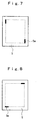
- Fig. 3 is a plan view of a resin cap 5 of the embodiment shown in Fig. 1, in which a protrusion 5a is provided so as to extend over the entire inner edge of the adhering surface of the resin cap 5.
- the cross-sectional view would be the same as Fig. 1.
- Fig. 4 is a plan view of a variation of the resin cap 5, in which protrusions 5a are provided so as to extend over the entire of the long sides and parts of the short sides of the resin cap 5.
- Fig. 5 is a plan view of another variation of the resin cap 5, in which protrusions 5a are provided at each corner of the resin cap 5.
- Fig. 6 is a plan view of a different variation of the resin cap 5, in which protrusions 5a are provided at the center parts of each of the sides of the resin cap 5.
- Fig. 7 is yet another variation of the resin cap 5, wherein protrusions 5a are provided at diagonally opposed positions on the long sides of the resin cap 5.
- Fig. 8 is yet another variation of the resin cap 5, wherein protrusions 5a are provided at diagonally opposite positions on the short sides of the resin cap 5.
- Fig. 9 is another variation of the present invention.
- protrusions 5a are provided along the outer edge of the adhering surface of the resin cap 5.
- Fig. 10 is another variation of the present invention.
- protrusions 1a are provided along the inner edge of the adhering surface of the resin substrate 5.
- the protrusions 5a shown in Fig. 3 to Fig. 8 can, if necessary, be provided in different positions than the positions shown in these drawings. While in the above-noted examples, the protrusions are provided along the outer edge or inner edge of the adhering surface, the protrusions can alternately be provided in the substantially center part of the adhering surface, in which case on the adhering surface a protruding part is provided on one side and a depression part is provided on the other side, these parts being provided at locations that enable the protruding part and the depression part to mutually fit together.
- the present invention achieves several effects, one of which is that, by providing a protrusion for positioning when fitting the resin cap and resin substrate together, the adhering positioning accuracy is improved.
- the reason for this is that it is possible to perform positioning by means of the protrusions.
- Another effect achieved by the present invention is that of eliminating shifting in position when the resin cap and the resin substrate are adhered and held together. The reason for this is that, in the same manner, positioning is possible by means of the protrusions.
Landscapes
- Physics & Mathematics (AREA)
- Acoustics & Sound (AREA)
- Surface Acoustic Wave Elements And Circuit Networks Thereof (AREA)
- Encapsulation Of And Coatings For Semiconductor Or Solid State Devices (AREA)
- Wire Bonding (AREA)
Abstract
Description
Claims (6)
- A molded package comprising a resin substrate (1), a resin cap (5) adhered thereto and a hollow portion (6) formed by said resin substrate and said resin cap, so as to protect a surface of a chip mounted onto said resin substrate by said hollow portion, wherein a protrusion (5a) for positioning said resin substrate and said resin cap is provided on at least one adhering surface of said resin substrate and said resin cap.
- A molded package according to claim 1, wherein said positioning protrusion (5a) is provided so that a surface of said protrusion makes contact with an inner surface of one of said resin substrate and said resin cap.
- A molded package according to claim 1, wherein said positioning protrusion (5a) is provided so that a surface of said protrusion makes contact with an outer surface of one of said resin substrate and said resin cap.
- A molded package according to claim 1, wherein said protrusion is provided along an outer edge of said adhering surface.
- A molded package according to claim 1, wherein said protrusion is provided along an inner edge of said adhering surface.
- A molded package according to claim 1, wherein said chip is a surface acoustic wave device.
Applications Claiming Priority (2)
| Application Number | Priority Date | Filing Date | Title |
|---|---|---|---|
| JP30500599A JP3430204B2 (en) | 1999-10-27 | 1999-10-27 | Hollow mold package equipment |
| JP30500599 | 1999-10-27 |
Publications (2)
| Publication Number | Publication Date |
|---|---|
| EP1096563A2 true EP1096563A2 (en) | 2001-05-02 |
| EP1096563A3 EP1096563A3 (en) | 2006-05-24 |
Family
ID=17939945
Family Applications (1)
| Application Number | Title | Priority Date | Filing Date |
|---|---|---|---|
| EP20000122170 Withdrawn EP1096563A3 (en) | 1999-10-27 | 2000-10-12 | Semiconductor package with premolded parts |
Country Status (3)
| Country | Link |
|---|---|
| EP (1) | EP1096563A3 (en) |
| JP (1) | JP3430204B2 (en) |
| KR (1) | KR100360783B1 (en) |
Cited By (1)
| Publication number | Priority date | Publication date | Assignee | Title |
|---|---|---|---|---|
| US7004325B2 (en) | 2001-05-08 | 2006-02-28 | Nec Compound Semiconductor Devices, Ltd. | Resin-molded package with cavity structure |
Families Citing this family (2)
| Publication number | Priority date | Publication date | Assignee | Title |
|---|---|---|---|---|
| WO2016067664A1 (en) * | 2014-10-28 | 2016-05-06 | 株式会社村田製作所 | Electronic device and method for producing same |
| JP2017147280A (en) * | 2016-02-15 | 2017-08-24 | 株式会社デンソー | Electronic circuit components |
Family Cites Families (4)
| Publication number | Priority date | Publication date | Assignee | Title |
|---|---|---|---|---|
| JPS6237950A (en) * | 1985-08-12 | 1987-02-18 | Matsushita Electronics Corp | Electronic-part mounting package |
| CA2047486C (en) * | 1990-07-21 | 2002-03-05 | Shigeru Katayama | Semiconductor device and method for manufacturing the same |
| US5436492A (en) * | 1992-06-23 | 1995-07-25 | Sony Corporation | Charge-coupled device image sensor |
| JPH06188672A (en) * | 1992-12-21 | 1994-07-08 | Toshiba Corp | Electronic component |
-
1999
- 1999-10-27 JP JP30500599A patent/JP3430204B2/en not_active Expired - Fee Related
-
2000
- 2000-10-12 EP EP20000122170 patent/EP1096563A3/en not_active Withdrawn
- 2000-10-26 KR KR1020000063070A patent/KR100360783B1/en not_active Expired - Fee Related
Cited By (2)
| Publication number | Priority date | Publication date | Assignee | Title |
|---|---|---|---|---|
| US7004325B2 (en) | 2001-05-08 | 2006-02-28 | Nec Compound Semiconductor Devices, Ltd. | Resin-molded package with cavity structure |
| US7187073B2 (en) | 2001-05-08 | 2007-03-06 | Nec Electronics Corporation | Resin-molded package with cavity structure |
Also Published As
| Publication number | Publication date |
|---|---|
| JP2001127184A (en) | 2001-05-11 |
| KR20010051250A (en) | 2001-06-25 |
| JP3430204B2 (en) | 2003-07-28 |
| EP1096563A3 (en) | 2006-05-24 |
| KR100360783B1 (en) | 2002-11-13 |
Similar Documents
| Publication | Publication Date | Title |
|---|---|---|
| KR100591375B1 (en) | Solid-state imaging device and method for manufacturing the same | |
| EP1494291A2 (en) | Solid-state imaging device and method for manufacturing the same | |
| KR100572388B1 (en) | Solid-state imaging device and its manufacturing method | |
| JP2002520627A (en) | Biometric sensor and method of manufacturing the sensor | |
| US20070018309A1 (en) | Image sensor package, optical glass used therein, and processing method of the optical glass | |
| KR20130083249A (en) | Semiconductor apparatus, image sensor package using the same | |
| EP1096563A2 (en) | Semiconductor package with premolded parts | |
| JPH10247695A (en) | Semiconductor device | |
| JPS63271969A (en) | Solid-state image sensor | |
| JPH0915074A (en) | Semiconductor pressure detecting device and manufacturing method thereof | |
| JP2006319130A (en) | Semiconductor device | |
| JPH08122179A (en) | Semiconductor pressure sensor and its production | |
| US20030122249A1 (en) | Semiconductor package with a sensor having a fastening insert | |
| JPH03104148A (en) | Package for semiconductor integrated circuit | |
| US20050104170A1 (en) | Semiconductor device and manufacturing method thereof | |
| JP2966746B2 (en) | Semiconductor device and manufacturing method thereof | |
| JP2851991B2 (en) | Optical coupling device | |
| JPS6223096Y2 (en) | ||
| JPH0428279A (en) | Semiconductor laser | |
| JP2002223003A (en) | Package molded body, manufacturing method thereof, and light emitting device | |
| JP2002162309A (en) | Pressure sensor | |
| KR20050109139A (en) | Method for assembling camera module | |
| JPWO2024203110A5 (en) | ||
| JPH0462478B2 (en) | ||
| US20030047815A1 (en) | Resin mold semiconductor device |
Legal Events
| Date | Code | Title | Description |
|---|---|---|---|
| PUAI | Public reference made under article 153(3) epc to a published international application that has entered the european phase |
Free format text: ORIGINAL CODE: 0009012 |
|
| AK | Designated contracting states |
Kind code of ref document: A2 Designated state(s): AT BE CH CY DE DK ES FI FR GB GR IE IT LI LU MC NL PT SE |
|
| AX | Request for extension of the european patent |
Free format text: AL;LT;LV;MK;RO;SI |
|
| RAP1 | Party data changed (applicant data changed or rights of an application transferred) |
Owner name: NIHON DEMPA KOGYO CO., LTD. |
|
| PUAL | Search report despatched |
Free format text: ORIGINAL CODE: 0009013 |
|
| AK | Designated contracting states |
Kind code of ref document: A3 Designated state(s): AT BE CH CY DE DK ES FI FR GB GR IE IT LI LU MC NL PT SE |
|
| AX | Request for extension of the european patent |
Extension state: AL LT LV MK RO SI |
|
| 17P | Request for examination filed |
Effective date: 20061025 |
|
| AKX | Designation fees paid |
Designated state(s): DE FI FR SE |
|
| 17Q | First examination report despatched |
Effective date: 20070425 |
|
| STAA | Information on the status of an ep patent application or granted ep patent |
Free format text: STATUS: THE APPLICATION IS DEEMED TO BE WITHDRAWN |
|
| 18D | Application deemed to be withdrawn |
Effective date: 20071105 |