EP1096548A2 - Semiconductor wafer processing apparatus comprising a wafer presence detector and method - Google Patents
Semiconductor wafer processing apparatus comprising a wafer presence detector and method Download PDFInfo
- Publication number
- EP1096548A2 EP1096548A2 EP00309089A EP00309089A EP1096548A2 EP 1096548 A2 EP1096548 A2 EP 1096548A2 EP 00309089 A EP00309089 A EP 00309089A EP 00309089 A EP00309089 A EP 00309089A EP 1096548 A2 EP1096548 A2 EP 1096548A2
- Authority
- EP
- European Patent Office
- Prior art keywords
- wafer
- cooling chamber
- chamber
- processing
- sensor
- Prior art date
- Legal status (The legal status is an assumption and is not a legal conclusion. Google has not performed a legal analysis and makes no representation as to the accuracy of the status listed.)
- Withdrawn
Links
Images


Classifications
-
- H—ELECTRICITY
- H10—SEMICONDUCTOR DEVICES; ELECTRIC SOLID-STATE DEVICES NOT OTHERWISE PROVIDED FOR
- H10P—GENERIC PROCESSES OR APPARATUS FOR THE MANUFACTURE OR TREATMENT OF DEVICES COVERED BY CLASS H10
- H10P72/00—Handling or holding of wafers, substrates or devices during manufacture or treatment thereof
- H10P72/04—Apparatus for manufacture or treatment
- H10P72/0451—Apparatus for manufacturing or treating in a plurality of work-stations
- H10P72/0452—Apparatus for manufacturing or treating in a plurality of work-stations characterised by the layout of the process chambers
- H10P72/0454—Apparatus for manufacturing or treating in a plurality of work-stations characterised by the layout of the process chambers surrounding a central transfer chamber
-
- H—ELECTRICITY
- H10—SEMICONDUCTOR DEVICES; ELECTRIC SOLID-STATE DEVICES NOT OTHERWISE PROVIDED FOR
- H10P—GENERIC PROCESSES OR APPARATUS FOR THE MANUFACTURE OR TREATMENT OF DEVICES COVERED BY CLASS H10
- H10P72/00—Handling or holding of wafers, substrates or devices during manufacture or treatment thereof
- H10P72/06—Apparatus for monitoring, sorting, marking, testing or measuring
- H10P72/0606—Position monitoring, e.g. misposition detection or presence detection
Definitions
- the present invention relates to the field of semiconductor fabrication and, more particularly, to a semiconductor wafer processing apparatus having a wafer presence detector.
- Chip production involves many steps of semiconductor wafer processing, including several steps in which metals are deposited onto the wafers in vacuum deposition chambers.
- Multiple chamber semiconductor wafer processing machines are in use in the industry for various processing steps in the fabrication of semiconductors. These machines may include several evacuable chambers, including processing chambers, transfer chambers, and loadlock chambers. The machines may perform several processes simultaneously on different wafers or sequentially on the same wafer.
- Such an apparatus as disclosed, for example, in U.S. Patent No. 5,882,165 to Maydan et al ., generally includes a mechanical transfer arm positioned in a transfer chamber for moving a wafer sequentially through several processing modules. At times, however, the transfer arm may fail to pick up the wafer to be transferred, or the wafer breaks during the transfer. Unfortunately, such accidental events may go undetected until the processing cycle is completed and an operator unloads wafers from the machine. Failure to notice a missing or broken wafer potentially results in contamination of an entire lot of wafers as they continue to be processed through the apparatus.
- the present invention advantageously provides a semiconductor wafer processing apparatus which can detect wafer status in the cooling chamber.
- an apparatus preferably comprising an optical sensor positioned adjacent the cooling chamber window and directed toward the wafer support for sensing wafer status.
- the apparatus also preferably includes a wafer processing chamber, a wafer transfer module positioned adjacent the processing chamber, a wafer cooling chamber having a window and a wafer support therein.
- the wafer cooling chamber is adjacent the wafer transfer module for receiving and cooling wafers downstream from the processing chamber.
- the optical sensor preferably includes an optical source and optical receiver.
- An aspect of the invention includes a method for semiconductor processing in a semiconductor wafer processing apparatus comprising at least one wafer processing chamber, a wafer transfer module positioned adjacent the at least one processing chamber, and a wafer cooling chamber adjacent the wafer transfer module.
- the method preferably comprises the steps of processing a wafer in the processing chamber, transferring the wafer from the processing chamber to the cooling chamber using the transfer module, and providing and using a sensor associated with the wafer cooling chamber for sensing wafer status in the cooling chamber.
- the apparatus 5 comprises at least one wafer processing chamber 21 , and five such chambers 21 , 23 , 25 , 27 and 29 in the illustrated embodiment
- the processing chambers may be for the deposition of materials, such as metals, as will be readily understood by those skilled in the art.
- a wafer transfer module 19 is positioned adjacent the processing chambers for transferring wafers from one chamber to another.
- the further operation of the wafer transfer module 19 will also be readily understood by those skilled in the art and requires no further discussion herein.
- a wafer cooling chamber 17 is positioned adjacent the wafer transfer module 19 for receiving and cooling wafers downstream from the processing chambers 29 .
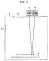
- the wafer cooling chamber 17 comprises a wafer support 31 and a window 33 adjacent the wafer support and in spaced apart relation therefrom.
- an optical sensor 35 is positioned adjacent the window 33 on the outside thereof, and is directed toward the wafer support 31 for sensing wafer 7 status.
- the sensor 35 is preferably positioned to sense wafer 7 status through the window 33 , wherein the wafer status includes at least one of presence, absence and breakage of the wafer 7 within the cooling chamber 17 .
- the optical sensor 35 preferably generates a signal responsive to wafer status.
- the apparatus 5 includes a controller 37 for controlling operation of the apparatus 5 . Accordingly, the optical sensor 35 is connected to the controller 37 for interrupting operation responsive to the wafer status signal.
- the cooling chamber 17 preferably also includes a cooling gas inlet port 39 for admitting cooling gas to cool the wafer 7 .
- the apparatus further comprises at least one load lock chamber 11 downstream from the cooling chamber 17 .
- Loadlock chambers 11 may function as both wafer inlet and wafer outlet chambers for the apparatus, as will be readily appreciated by those skilled in the art.
- Chamber 13 is also a wafer transfer chamber associated with the loadlock chambers 11 .
- the processing chambers are arranged about a portion of an imaginary circle so that a wafer 7 may be transferred from one chamber to another sequentially by the transfer module 19 for processing, such as cleaning or metal deposition, and finally transferred for cooling in the cooling chamber 17 .
- the optical sensor 35 preferably includes an optical source 41 and an optical receiver 43 cooperating therewith for sensing wafer 7 status.
- the optical sensor 35 may also include a plurality of optical sources and optical receivers cooperating to sense wafer status. Such a plurality of optical sources and optical receivers would be particularly useful in sensing a greater area of the wafer 7 to improve detection of breakage.
- the optical sensor 35 may also be positioned within the cooling chamber 17 itself.
- the cooling chamber 17 also further comprises an access port 45 for allowing operator access to the chamber. Skilled artisans will appreciate that such an access port may be positioned on the cooling chamber as practicable.
- Another aspect of the invention is directed to a method for semiconductor processing in a semiconductor wafer processing apparatus comprising at least one wafer processing chamber, a wafer transfer module positioned adjacent the at least one processing chamber, and a wafer cooling chamber adjacent the wafer transfer module.
- the method starts (Block 50) by the step of processing a wafer in the processing chamber (Block 52), transferring the wafer from the processing chamber to the cooling chamber (Block 54) using the transfer module, and providing and using a sensor associated with the wafer cooling chamber for sensing wafer status in the cooling chamber (Block 56).
- wafer status monitored includes at least one of presence or absence of the wafer (Block 58), and breakage of the wafer (Block 60) within said cooling chamber. Responsive to the sensing step, the sensor generates a wafer status signal. If the sensing step indicates a missing wafer, or a broken wafer (Block 63), the appropriate trouble signal is generated, operation is interrupted (Block 65), and the method stops (Block 66). If the sensing step indicates a wafer is present and unbroken, the appropriate signal is generated (Block 62), and processing continues until finished (Block 64), whereupon the method stops (Block 66).
Landscapes
- Chemical Vapour Deposition (AREA)
- Container, Conveyance, Adherence, Positioning, Of Wafer (AREA)
Abstract
An apparatus for processing semiconductor wafers
includes at least one wafer processing chamber, a wafer
transfer module positioned adjacent the processing chamber,
and a wafer cooling chamber having a window and a wafer
support therein and being adjacent the wafer transfer
module for receiving and cooling wafers downstream from the
processing chamber. The apparatus also includes an optical
sensor positioned adjacent the cooling chamber window and
directed toward the wafer support for sensing wafer status.
The sensor generates a signal responsive to sensed wafer
status, and operation is interrupted if the wafer is
missing or broken.
Description
- The present invention relates to the field of semiconductor fabrication and, more particularly, to a semiconductor wafer processing apparatus having a wafer presence detector.
- Processing of semiconductor wafers is an essential step in the manufacture of integrated circuits, also known as ICs or simply, chips. A number of ICs may be manufactured on a semiconductor wafer, which is then cut into individual chips. Chip production involves many steps of semiconductor wafer processing, including several steps in which metals are deposited onto the wafers in vacuum deposition chambers.
- Multiple chamber semiconductor wafer processing machines are in use in the industry for various processing steps in the fabrication of semiconductors. These machines may include several evacuable chambers, including processing chambers, transfer chambers, and loadlock chambers. The machines may perform several processes simultaneously on different wafers or sequentially on the same wafer. Such an apparatus as disclosed, for example, in U.S. Patent No. 5,882,165 to Maydan et al., generally includes a mechanical transfer arm positioned in a transfer chamber for moving a wafer sequentially through several processing modules. At times, however, the transfer arm may fail to pick up the wafer to be transferred, or the wafer breaks during the transfer. Unfortunately, such accidental events may go undetected until the processing cycle is completed and an operator unloads wafers from the machine. Failure to notice a missing or broken wafer potentially results in contamination of an entire lot of wafers as they continue to be processed through the apparatus.
- With the foregoing in mind, the present invention advantageously provides a semiconductor wafer processing apparatus which can detect wafer status in the cooling chamber.
- This and other objects, features and advantages in accordance with the present invention are provided by an apparatus preferably comprising an optical sensor positioned adjacent the cooling chamber window and directed toward the wafer support for sensing wafer status. The apparatus also preferably includes a wafer processing chamber, a wafer transfer module positioned adjacent the processing chamber, a wafer cooling chamber having a window and a wafer support therein. The wafer cooling chamber is adjacent the wafer transfer module for receiving and cooling wafers downstream from the processing chamber. The optical sensor preferably includes an optical source and optical receiver.
- An aspect of the invention includes a method for semiconductor processing in a semiconductor wafer processing apparatus comprising at least one wafer processing chamber, a wafer transfer module positioned adjacent the at least one processing chamber, and a wafer cooling chamber adjacent the wafer transfer module. The method preferably comprises the steps of processing a wafer in the processing chamber, transferring the wafer from the processing chamber to the cooling chamber using the transfer module, and providing and using a sensor associated with the wafer cooling chamber for sensing wafer status in the cooling chamber.
- Some of the features, advantages, and benefits of the present invention having been stated, others will become apparent as the description proceeds when taken in conjunction with the accompanying drawings in which:
- FIG. 1 is a schematic top plan view of the apparatus; and
- FIG. 2 is a schematic cross sectional view of the cooling chamber as shown in FIG. 1; and
- FIG. 3 is a flow chart illustrating the method according to an embodiment of the present invention.
-
- The present invention will now be described more fully hereinafter with reference to the accompanying drawings, in which preferred embodiments of the invention are shown. This invention may, however, be embodied in many different forms and should not be construed as limited to the illustrated embodiments set forth herein. Rather, these illustrated embodiments are provided so that this disclosure will be thorough and complete, and will fully convey the scope of the invention to those skilled in the art.
- Referring to FIGS. 1 and 2, an
apparatus 5 for processing asemiconductor wafer 7 is initially described. Theapparatus 5 comprises at least onewafer processing chamber 21, and fivesuch chambers - A
wafer transfer module 19 is positioned adjacent the processing chambers for transferring wafers from one chamber to another. The further operation of thewafer transfer module 19 will also be readily understood by those skilled in the art and requires no further discussion herein. - A
wafer cooling chamber 17 is positioned adjacent thewafer transfer module 19 for receiving and cooling wafers downstream from theprocessing chambers 29. Thewafer cooling chamber 17 comprises awafer support 31 and awindow 33 adjacent the wafer support and in spaced apart relation therefrom. In addition, anoptical sensor 35 is positioned adjacent thewindow 33 on the outside thereof, and is directed toward thewafer support 31 for sensingwafer 7 status. - The
sensor 35, is preferably positioned to sensewafer 7 status through thewindow 33, wherein the wafer status includes at least one of presence, absence and breakage of thewafer 7 within thecooling chamber 17. Theoptical sensor 35 preferably generates a signal responsive to wafer status. In a preferred embodiment, theapparatus 5 includes acontroller 37 for controlling operation of theapparatus 5. Accordingly, theoptical sensor 35 is connected to thecontroller 37 for interrupting operation responsive to the wafer status signal. Thecooling chamber 17 preferably also includes a coolinggas inlet port 39 for admitting cooling gas to cool thewafer 7. - In a preferred embodiment the apparatus further comprises at least one
load lock chamber 11 downstream from thecooling chamber 17.Loadlock chambers 11, however, may function as both wafer inlet and wafer outlet chambers for the apparatus, as will be readily appreciated by those skilled in the art. -
Chamber 13 is also a wafer transfer chamber associated with theloadlock chambers 11. In the illustrated embodiment it is also noted that the processing chambers are arranged about a portion of an imaginary circle so that awafer 7 may be transferred from one chamber to another sequentially by thetransfer module 19 for processing, such as cleaning or metal deposition, and finally transferred for cooling in thecooling chamber 17. - As shown schematically in FIG. 2, the
optical sensor 35 preferably includes anoptical source 41 and anoptical receiver 43 cooperating therewith for sensingwafer 7 status. Those skilled in the art will understand that theoptical sensor 35 may also include a plurality of optical sources and optical receivers cooperating to sense wafer status. Such a plurality of optical sources and optical receivers would be particularly useful in sensing a greater area of thewafer 7 to improve detection of breakage. In an alternate embodiment of the invention, theoptical sensor 35 may also be positioned within thecooling chamber 17 itself. As also shown in FIG. 2, thecooling chamber 17 also further comprises anaccess port 45 for allowing operator access to the chamber. Skilled artisans will appreciate that such an access port may be positioned on the cooling chamber as practicable. - Another aspect of the invention, explained with reference to the flow chart of FIG. 3, is directed to a method for semiconductor processing in a semiconductor wafer processing apparatus comprising at least one wafer processing chamber, a wafer transfer module positioned adjacent the at least one processing chamber, and a wafer cooling chamber adjacent the wafer transfer module. The method starts (Block 50) by the step of processing a wafer in the processing chamber (Block 52), transferring the wafer from the processing chamber to the cooling chamber (Block 54) using the transfer module, and providing and using a sensor associated with the wafer cooling chamber for sensing wafer status in the cooling chamber (Block 56). In the method, wafer status monitored includes at least one of presence or absence of the wafer (Block 58), and breakage of the wafer (Block 60) within said cooling chamber. Responsive to the sensing step, the sensor generates a wafer status signal. If the sensing step indicates a missing wafer, or a broken wafer (Block 63), the appropriate trouble signal is generated, operation is interrupted (Block 65), and the method stops (Block 66). If the sensing step indicates a wafer is present and unbroken, the appropriate signal is generated (Block 62), and processing continues until finished (Block 64), whereupon the method stops (Block 66).
- Many modifications and other embodiments of the invention will come to the mind of one skilled in the art having the benefit of the teachings presented in the foregoing descriptions and the associated drawings. Therefore, it is to be understood that the invention is not to be limited to the specific embodiments disclosed.
Claims (20)
- A semiconductor wafer processing apparatus comprising:at least one wafer processing chamber;a wafer transfer module positioned adjacent said at least one processing chamber;a wafer cooling chamber adjacent said wafer transfer module for receiving and cooling wafers downstream from said at least one processing chamber; anda sensor associated with said wafer cooling chamber for sensing wafer status.
- The apparatus of claim 1 wherein the wafer status includes at least one of presence, absence and breakage of the wafer within said cooling chamber.
- The apparatus of claim 1 or claim 2 wherein said sensor comprises an optical source and an optical receiver cooperating therewith for sensing wafer status.
- The apparatus of any of the preceding claims wherein said sensor generates a wafer status signal.
- The apparatus of claim 4 further comprising a controller for controlling operation of the apparatus, and wherein said sensor is connected to said controller for interrupting operation responsive to the wafer status signal.
- The apparatus of any of the preceding claims wherein said sensor is positioned within said cooling chamber.
- The apparatus of any of claims 1 to 5 wherein said cooling chamber includes a window, and wherein said sensor is positioned outside said cooling chamber adjacent said window.
- The apparatus of claim 3 wherein said optical source and said optical receiver are positioned outside said cooling chamber.
- The apparatus of any of claims 1 to 5 wherein:said wafer cooling chamber includes a wafer support and a window adjacent said wafer support; andsaid sensor is an optical sensor positioned outside said window and directed toward said wafer support.
- The apparatus of any of the preceding claims wherein said cooling chamber includes a cooling gas inlet port for admitting cooling gas to cool the wafer.
- The apparatus of any of the preceding claims further comprising at least one load lock chamber downstream from said cooling chamber.
- The apparatus of any of the preceding claims wherein said at least one processing chamber comprises at least one metal deposition chamber.
- The apparatus of any of the preceding claims wherein said cooling chamber further comprises an access port for allowing operator access.
- The apparatus of any of the preceding claims wherein:there is a plurality of said wafer processing chambers having respective wafer receiving openings arranged about at least a portion of an imaginary circle; andsaid wafer transfer module is positioned within the imaginary circle.
- A method for semiconductor processing in a semiconductor wafer processing apparatus comprising at least one wafer processing chamber, a wafer transfer module positioned adjacent the at least one processing chamber, and a wafer cooling chamber adjacent the wafer transfer module, the method comprising the steps of:processing a wafer in the at least one processing chamber;transferring the wafer from the at least one processing chamber to the cooling chamber using the transfer module; andproviding and using a sensor associated with the wafer cooling chamber for sensing wafer status in the cooling chamber.
- The method of claim 15 wherein the wafer status includes at least one of presence, absence and breakage of the wafer within said cooling chamber.
- The method of claim 15 or claim 16 wherein the sensor generates a wafer status signal.
- The method of claim 17 further comprising the step of interrupting operation of the apparatus responsive to the wafer status signal.
- The method of any of claims 15 to 18 wherein the cooling chamber includes a window, and wherein the step of providing the sensor comprises positioning the sensor outside the cooling chamber adjacent the window.
- The method of any of claims 15 to 19 wherein the step of providing the sensor comprises providing an optical sensor including an optical source and an optical receiver cooperating therewith for sensing wafer status.
Applications Claiming Priority (2)
| Application Number | Priority Date | Filing Date | Title |
|---|---|---|---|
| US430768 | 1989-10-31 | ||
| US43076899A | 1999-10-29 | 1999-10-29 |
Publications (1)
| Publication Number | Publication Date |
|---|---|
| EP1096548A2 true EP1096548A2 (en) | 2001-05-02 |
Family
ID=23708946
Family Applications (1)
| Application Number | Title | Priority Date | Filing Date |
|---|---|---|---|
| EP00309089A Withdrawn EP1096548A2 (en) | 1999-10-29 | 2000-10-16 | Semiconductor wafer processing apparatus comprising a wafer presence detector and method |
Country Status (1)
| Country | Link |
|---|---|
| EP (1) | EP1096548A2 (en) |
Cited By (3)
| Publication number | Priority date | Publication date | Assignee | Title |
|---|---|---|---|---|
| KR100454393B1 (en) * | 2001-12-18 | 2004-10-26 | 코스텍시스템(주) | Multi Vertical-type Single wafer-System apparatus for processing semiconductor wafer |
| TWI549218B (en) * | 2015-02-17 | 2016-09-11 | 力鼎精密股份有限公司 | Semiconductor apparatus and the processing chamber and the wafer transfer method thereof |
| CN112233992A (en) * | 2020-09-10 | 2021-01-15 | 上海华力集成电路制造有限公司 | Wafer fragment detection device and method of using the same |
-
2000
- 2000-10-16 EP EP00309089A patent/EP1096548A2/en not_active Withdrawn
Cited By (3)
| Publication number | Priority date | Publication date | Assignee | Title |
|---|---|---|---|---|
| KR100454393B1 (en) * | 2001-12-18 | 2004-10-26 | 코스텍시스템(주) | Multi Vertical-type Single wafer-System apparatus for processing semiconductor wafer |
| TWI549218B (en) * | 2015-02-17 | 2016-09-11 | 力鼎精密股份有限公司 | Semiconductor apparatus and the processing chamber and the wafer transfer method thereof |
| CN112233992A (en) * | 2020-09-10 | 2021-01-15 | 上海华力集成电路制造有限公司 | Wafer fragment detection device and method of using the same |
Similar Documents
| Publication | Publication Date | Title |
|---|---|---|
| US8588950B2 (en) | Substrate processing apparatus | |
| US6424733B2 (en) | Method and apparatus for inspecting wafers | |
| US20120226475A1 (en) | Substrate processing system, management apparatus, data analysis method | |
| US8126588B2 (en) | Method and system for controlling transport sequencing in a process tool by a look-ahead mode | |
| CN110858555B (en) | Substrate transfer module and substrate transfer method | |
| JP2014060412A (en) | Semiconductor manufacturing device | |
| WO2005010978A1 (en) | Method and apparatus for performing metrology dispatching based upon fault detection | |
| JP4068404B2 (en) | Substrate processing system, substrate processing apparatus, substrate processing method, program, and recording medium | |
| TW202209535A (en) | Wafer cassette device, semiconductor processing machine and wafer detecting method characterized by identifying in real time the abnormal conditions of the wafer in the wafer cassette to reduce the crash rate and greatly improving the yield of wafers | |
| US20240175788A1 (en) | Method for detecting environmental parameter in semiconductor fabrication facility | |
| US7130762B2 (en) | Method and system for handling substrates in a production line including a cluster tool and a metrology tool | |
| EP1082755A1 (en) | A wafer buffer station and a method for a per-wafer transfer between work stations | |
| JPH085542A (en) | Method and device for manufacturing semiconductor device | |
| US12224199B2 (en) | Semiconductor manufacturing apparatus and method for manufacturing semiconductor device | |
| JP2005286102A (en) | Vacuum processing apparatus and vacuum processing method | |
| JP4302491B2 (en) | Single wafer vacuum processing equipment | |
| EP1098351A2 (en) | Apparatus detecting misalignment of processing semiconductor wafers in a cassette and associated methods | |
| US20020028131A1 (en) | Vacuum processing apparatus and semiconductor manufacturing line using the same | |
| EP1747575B1 (en) | Inter-process sensing of wafer outcome | |
| US5604134A (en) | Particle monitoring method for plasma reactors with moving gas distribution housings | |
| KR20060084926A (en) | Wafer processing equipment | |
| KR20050045339A (en) | Apparatus for transporting wafer | |
| JPH03257945A (en) | Manufacture device for semiconductor | |
| KR100495419B1 (en) | Semiconductor manufacturing device | |
| KR20060121331A (en) | Semiconductor manufacturing equipment having one fork robot arm and wafer transfer method thereof |
Legal Events
| Date | Code | Title | Description |
|---|---|---|---|
| PUAI | Public reference made under article 153(3) epc to a published international application that has entered the european phase |
Free format text: ORIGINAL CODE: 0009012 |
|
| AK | Designated contracting states |
Kind code of ref document: A2 Designated state(s): AT BE CH CY DE DK ES FI FR GB GR IE IT LI LU MC NL PT SE |
|
| AX | Request for extension of the european patent |
Free format text: AL;LT;LV;MK;RO;SI |
|
| STAA | Information on the status of an ep patent application or granted ep patent |
Free format text: STATUS: THE APPLICATION HAS BEEN WITHDRAWN |
|
| 18W | Application withdrawn |
Withdrawal date: 20010717 |