EP1096321A1 - Light exposure method - Google Patents
Light exposure method Download PDFInfo
- Publication number
- EP1096321A1 EP1096321A1 EP00402998A EP00402998A EP1096321A1 EP 1096321 A1 EP1096321 A1 EP 1096321A1 EP 00402998 A EP00402998 A EP 00402998A EP 00402998 A EP00402998 A EP 00402998A EP 1096321 A1 EP1096321 A1 EP 1096321A1
- Authority
- EP
- European Patent Office
- Prior art keywords
- high molecular
- compound
- resist layer
- light exposure
- resist
- Prior art date
- Legal status (The legal status is an assumption and is not a legal conclusion. Google has not performed a legal analysis and makes no representation as to the accuracy of the status listed.)
- Withdrawn
Links
Images
Classifications
-
- G—PHYSICS
- G03—PHOTOGRAPHY; CINEMATOGRAPHY; ANALOGOUS TECHNIQUES USING WAVES OTHER THAN OPTICAL WAVES; ELECTROGRAPHY; HOLOGRAPHY
- G03F—PHOTOMECHANICAL PRODUCTION OF TEXTURED OR PATTERNED SURFACES, e.g. FOR PRINTING, FOR PROCESSING OF SEMICONDUCTOR DEVICES; MATERIALS THEREFOR; ORIGINALS THEREFOR; APPARATUS SPECIALLY ADAPTED THEREFOR
- G03F7/00—Photomechanical, e.g. photolithographic, production of textured or patterned surfaces, e.g. printing surfaces; Materials therefor, e.g. comprising photoresists; Apparatus specially adapted therefor
- G03F7/20—Exposure; Apparatus therefor
- G03F7/2037—Exposure with X-ray radiation or corpuscular radiation, through a mask with a pattern opaque to that radiation
- G03F7/2039—X-ray radiation
-
- H—ELECTRICITY
- H10—SEMICONDUCTOR DEVICES; ELECTRIC SOLID-STATE DEVICES NOT OTHERWISE PROVIDED FOR
- H10P—GENERIC PROCESSES OR APPARATUS FOR THE MANUFACTURE OR TREATMENT OF DEVICES COVERED BY CLASS H10
- H10P76/00—Manufacture or treatment of masks on semiconductor bodies, e.g. by lithography or photolithography
-
- G—PHYSICS
- G03—PHOTOGRAPHY; CINEMATOGRAPHY; ANALOGOUS TECHNIQUES USING WAVES OTHER THAN OPTICAL WAVES; ELECTROGRAPHY; HOLOGRAPHY
- G03F—PHOTOMECHANICAL PRODUCTION OF TEXTURED OR PATTERNED SURFACES, e.g. FOR PRINTING, FOR PROCESSING OF SEMICONDUCTOR DEVICES; MATERIALS THEREFOR; ORIGINALS THEREFOR; APPARATUS SPECIALLY ADAPTED THEREFOR
- G03F7/00—Photomechanical, e.g. photolithographic, production of textured or patterned surfaces, e.g. printing surfaces; Materials therefor, e.g. comprising photoresists; Apparatus specially adapted therefor
- G03F7/004—Photosensitive materials
- G03F7/075—Silicon-containing compounds
- G03F7/0757—Macromolecular compounds containing Si-O, Si-C or Si-N bonds
-
- Y—GENERAL TAGGING OF NEW TECHNOLOGICAL DEVELOPMENTS; GENERAL TAGGING OF CROSS-SECTIONAL TECHNOLOGIES SPANNING OVER SEVERAL SECTIONS OF THE IPC; TECHNICAL SUBJECTS COVERED BY FORMER USPC CROSS-REFERENCE ART COLLECTIONS [XRACs] AND DIGESTS
- Y10—TECHNICAL SUBJECTS COVERED BY FORMER USPC
- Y10S—TECHNICAL SUBJECTS COVERED BY FORMER USPC CROSS-REFERENCE ART COLLECTIONS [XRACs] AND DIGESTS
- Y10S430/00—Radiation imagery chemistry: process, composition, or product thereof
- Y10S430/167—X-ray
-
- Y—GENERAL TAGGING OF NEW TECHNOLOGICAL DEVELOPMENTS; GENERAL TAGGING OF CROSS-SECTIONAL TECHNOLOGIES SPANNING OVER SEVERAL SECTIONS OF THE IPC; TECHNICAL SUBJECTS COVERED BY FORMER USPC CROSS-REFERENCE ART COLLECTIONS [XRACs] AND DIGESTS
- Y10—TECHNICAL SUBJECTS COVERED BY FORMER USPC
- Y10S—TECHNICAL SUBJECTS COVERED BY FORMER USPC CROSS-REFERENCE ART COLLECTIONS [XRACs] AND DIGESTS
- Y10S430/00—Radiation imagery chemistry: process, composition, or product thereof
- Y10S430/167—X-ray
- Y10S430/168—X-ray exposure process
Definitions
- This invention relates to a light exposure method for ultra-fine processing in the field of a semiconductor.
- the so-called lithographic technique is indispensable.
- development of a new light exposure technique employing an extreme ultraviolet (EUV) rays in the vicinity of the wavelength of 7 to 16 nm, in addition to the ultraviolet rays by a conventional mercury lamp or excimer laser, is going on briskly in order to improve optical resolution to cope with shorter wavelengths used for light exposure to achieve the ultra-fine processing.
- EUV extreme ultraviolet
- the wavelength range of the extreme ultraviolet (EUV) suffers a problem that, within the wavelength range of the ultraviolet (EUV), usual resist materials undergo significant optical absorption, such that the illuminated light cannot reach the deeper portion in the resist layer to deteriorate the resist pattern.
- This deterioration in the resist pattern hampers ultra-fine processing and hence is desirably to be improved.
- EUV extreme ultraviolet
- a light exposure method in which a resist layer is exposed selectively to X-rays, vacuum ultraviolet rays, extreme ultraviolet rays or soft X-rays to pattern the resist layer to a pre-set shape, wherein, as a high molecular material of the resist layer, a high molecular material obtained by replacing at least a portion of hydrogen atoms of a pre-existing resist material by a substituent containing an alkyl group and/or a substituent containing an aromatic ring.
- the resist material herein means the totality of resist materials known prior to filing of the present application.
- the presence of oxygen atoms is indispensable for displaying resist characteristics.
- the portions subjected to a certain chemical reaction due to light illuminated thereon to produce changes in the physical values of the illuminated and non-illuminated portions to demonstrate resist characteristics are groups necessarily containing oxygen, such as ester-, phenolic-, alcoholic- or carboxylic groups.
- optical absorption of oxygen is larger than that of carbon or hydrogen, and is responsible for lowering of the light transmittance of the high molecular materials.
- the optical absorption per oxygen atom is as large as approximately thrice that of carbon atoms, and approximately 50 to 100 times that of the hydrogen atoms.
- the proportion of oxygen atoms in the atoms making up the high molecular materials is relatively smaller to suppress the optical absorption of the high molecular material in its entirety.
- a resist pattern of a desirable shape may be produced to enable ultra-fine processing more elaborate than is possible with the conventional method.
- the film thickness of the resist layer can be increased by employing a high molecular material exhibiting high transparency, thereby improving resistance to etching of the resist layer.
- EUV extreme ultraviolet
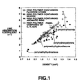
- Fig. 1 is a graph illustrating the of line absorption coefficients and density distribution of a variety of high molecular materials.
- the light exposure method of the present invention is applied to, for example, the processing of ultra-fine patterns in a semiconductor device.
- the method includes a step of coating a resist layer exhibiting the photosensitive action on a substrate, a step of selectively exposing and thereby photosensitizing the resist layer to X-rays, vacuum ultraviolet rays, extreme ultraviolet (EUV) or soft X-rays and a step of developing the resist layer to produce a pre-set pattern.
- EUV extreme ultraviolet
- X-rays for light exposure X-rays of arbitrary wavelengths may be used.
- extreme ultraviolet (soft X-rays) with a specified wavelength of 7 to 16 nm it is possible to realize light exposure with a resolution higher than is possible with the conventional method.
- the high molecular material, used as the resist layer includes e.g., novolak resins, polyhydroxy styrene resins, acrylic resins, siloxane resins containing ester or phenolic groups, silsesqui oxanoic resins or polycycloolefinic resins, as a basic skeleton.
- those portions undergoing chemical reactions due to the illuminated light to cause changes in the physical values of the illuminated and non-illuminated portions to manifest characteristics as a resist material are groups, such as ester-, phenolic-, alcoholic- or carboxylic groups.
- the order of the optical absorption in the wavelength range of the extreme ultraviolet (EUV) is Si > F > O > C > H for 7 nm, F > Si > O > C > H for 10 and 11 nm and F > Si > O > C > H for 13 and 16 nm. That is, the oxygen content is not favorable insofar as optical absorption in the wavelength range of the extreme ultraviolet (EUV) of the high molecular materials is concerned.
- the proportion of carbon and hydrogen atoms to oxygen atoms is increased to effect relative thinning of the oxygen atoms in order to lower the absorption in the wavelength range ofthe extreme ultraviolet (EUV) of the high molecular material used as a resist material to realize the relative lowering of the oxygen atoms.
- EUV extreme ultraviolet
- part or all of the hydrogen atoms of the aforementioned resist materials having the aforementioned skeleton structure is replaced by alkyl group and/or an aromatic group.
- alkyl group or the aromatic ring may directly be substituted for hydrogen atoms.
- the alkyl group or the aromatic ring may be introduced by replacing the hydrogen atoms by substituents containing alkyl groups or the aromatic rings. Any suitable substituents containing alkyl groups or aromatic rings may be used, whilst the number of carbon atoms in the alkyl group is arbitrary.
- the basic structure of the high molecular materials (pre-existing resist material) to be subjected to substitution may already own an alkyl group(s) or an aromatic ring(s). It is because the absorption coefficients in the wavelength of the extreme ultraviolet (EUV) are lowered by further replacing part or all of the hydrogen atoms in the high molecular material owning the alkyl group(s) or the aromatic ring(s) from the outset by the alkyl group(s) or the aromatic ring(s).
- EUV extreme ultraviolet
- the proportion of the carbon and hydrogen atoms may be increased to render it possible to furnish a high molecular material having a low absorption coefficient in the extreme ultraviolet wavelength range.
- the density of the resist material in its entirety is markedly increased by increasing the proportion of the carbon or hydrogen atoms, the possibility is high that, conversely, the absorption at the extreme ultraviolet wavelength is increased.
- the line absorption coefficient in the X-ray wavelength range is preferably not larger than 3.80 ⁇ m -1 . It is noted that, if the extreme ultraviolet light is used, the X-ray wavelength range reads extreme ultraviolet wavelength range.
- the transmittance of the resist layer for the film thickness of 300 nm is of a sufficiently high value of approximately 30% or higher. If the line absorption coefficient exceeds 3.80 ⁇ -1 , with the transmittance being of a smaller value, there is a risk that the illuminated light cannot reach the deeper area in the resist layer, with the result that a resist pattern of the desirable rectangular resist pattern cannot be produced.
- the present inventors have theoretically derived the line absorption coefficient of the high molecular materials at a wavelength of 13 nm in accordance with the following method.
- the error of the density of the high molecular materials calculated by this technique is known to be 2.2% on an average. So, the precision in prediction of the line absorption coefficient at a wavelength of 13 nm is also 2.2% on an average.
- An acrylic high molecular material (compound 1) was used as a basic high molecular material (pre-existing resist material), and line absorption coefficients on substituting propyl-, ethyl-, butyl- or hexyl groups for hydrogen atoms in this pre-existing resist material were found on calculations.
- Table 1 shows calculated results of the line absorption coefficients ( wavelength: 13 nm) of the respective compounds. 40. compounds line absorption coefficients compound 1 4.80 ⁇ -1 compound 2 3.81 ⁇ -1 compound 3 3.84 ⁇ -1 compound 4 4.02 ⁇ -1 compound 5 3.58 ⁇ -1 compound 6 3.66 ⁇ -1 compound 7 3.38 ⁇ -1
- the line absorption coefficients at the wavelength of 13 nm are decreased.
- the line absorption coefficient is not larger than 3.80 ⁇ -1 in case of substitution by butyl or hexyl groups.
- a polyvinylphenolic high polymer material (compound 8) was used as a basic high polymer material (pre-existing resist material) and line absorption coefficients of compounds obtained on substituting propyl groups for hydrogen atoms at various positions of the basic high polymer material were found on calculations.
- Table 2 shows calculated results of the line absorption coefficients ( wavelength: 13 nm) of the respective compounds.
- Compound 9 3.23 ⁇ -1
- Compound 10 3.23 ⁇ -1
- Compound 11 3.25 ⁇ -1
- a siloxane based high polymer material (compound 12) was used as a basic high polymer material and its hydrogen atom was replaced by a propyl group to give a compound 13 or by an aminopropyl group to give a compound 14.
- the structures of the respective compounds are as shown by the following chemical formulas 12 to 14:
- Table 3 shows calculated results of the line absorption coefficients ( wavelength: 13 nm) of the respective compounds.
- Compounds line absorption coefficient Compound 12 3.86 ⁇ -1
- Compound 14 3.70 ⁇ -1
- An acrylic high polymer material (compound 15) was used as a basic high polymer material (pre-existing resist material) and its hydrogen atom was replaced by a phenyl group and a naphthalene group to find the line absorption coefficients of the resulting compounds on calculations.
- Table 4 shows calculated results of the line absorption coefficients (wavelength: 13 nm) of the respective compounds.
- Compounds line absorption coefficient Compound 15 4.80 ⁇ -1
- Compound 16 4.06 ⁇ -1
- Compound 17 3.96 ⁇ -1
- a polyvinylphenolic high polymer material (compound 18) was used as a basic high polymer material (pre-existing resist material) and line absorption coefficients of compounds obtained on substituting phenyl-, naphthalene- and methylphenyl groups for hydrogen atoms were found on calculations.
- Table 5 shows calculated results of the line absorption coefficients ( wavelength: 13 nm) of the respective compounds.
- Compound 19 3.49 ⁇ -1
- Compound 20 3.50 ⁇ -1
- Compound 21 3.35 ⁇ -1
- a siloxane based high polymer material (compound 22) was used as a basic high polymer material (pre-existing resist material) and its hydrogen atom was replaced by a phenyl group or a naphthalene group to give compounds 23, 24, respectively, and the line absorption coefficients of these compounds were calculated.
- Table 6 shows calculated results of the line absorption coefficients ( wavelength: 13 nm) of the respective compounds.
- the line absorption coefficient is larger than in the usual high polymer material.
- the line absorption coefficient at the wavelength of 13 nm is lowered by substituting an alkyl group or an aromatic ring, such as phenyl or naphthalene groups, for a hydrogen atom of the high polymer material. That is, by substitution by alkyl groups or aromatic rings, it is possible to realize a material superior in transparency for use as a resist material.
- acrylic high molecular materials polyvinyl phenolic high molecular materials and siloxane-based high molecular materials are used as illustrative of the high molecular materials. These compounds are, however, merely illustrative such that any other suitable materials, such as other vinyl-based high molecular materials, polyimide based high molecular materials or the fluorine-based high molecular materials may also be used.
- substituents are also not limited to those shown in the Examples since any suitable alkyl groups, such as methyl, pentyl or hexyl substituents, may also be used.
- any suitable aromatic rings may be used as substituents, such as phenyl-, naphthalene-, anthracene-, biphenyl- or triphenyl substituents, may be used as aromatic ring substituents.
Landscapes
- Physics & Mathematics (AREA)
- General Physics & Mathematics (AREA)
- Health & Medical Sciences (AREA)
- Toxicology (AREA)
- Spectroscopy & Molecular Physics (AREA)
- Exposure And Positioning Against Photoresist Photosensitive Materials (AREA)
- Materials For Photolithography (AREA)
- Exposure Of Semiconductors, Excluding Electron Or Ion Beam Exposure (AREA)
Abstract
Description
- This invention relates to a light exposure method for ultra-fine processing in the field of a semiconductor.
- In e.g., the field of a semiconductor, establishment of a new processing technique providing for ultra-fine processing to a size not larger than 0.1 µm is incumbent with the tendency towards high integration degree of semiconductor devices.
- In processing an ultra-fine pattern, the so-called lithographic technique is indispensable. At present, development of a new light exposure technique employing an extreme ultraviolet (EUV) rays in the vicinity of the wavelength of 7 to 16 nm, in addition to the ultraviolet rays by a conventional mercury lamp or excimer laser, is going on briskly in order to improve optical resolution to cope with shorter wavelengths used for light exposure to achieve the ultra-fine processing.
- However, the wavelength range of the extreme ultraviolet (EUV) suffers a problem that, within the wavelength range of the ultraviolet (EUV), usual resist materials undergo significant optical absorption, such that the illuminated light cannot reach the deeper portion in the resist layer to deteriorate the resist pattern.
- This deterioration in the resist pattern hampers ultra-fine processing and hence is desirably to be improved.
- It is therefore an object ofthe present invention to eliminate the aforementioned problem and to provide a light exposure method in which the problem pertinent to light transmittance of a resist layer in the wavelength range of the extreme ultraviolet (EUV) may be eliminated to enable more elaborate ultra-fine processing.
- According to the present invention, there is provided a light exposure method in which a resist layer is exposed selectively to X-rays, vacuum ultraviolet rays, extreme ultraviolet rays or soft X-rays to pattern the resist layer to a pre-set shape, wherein, as a high molecular material of the resist layer, a high molecular material obtained by replacing at least a portion of hydrogen atoms of a pre-existing resist material by a substituent containing an alkyl group and/or a substituent containing an aromatic ring.
- The resist material herein means the totality of resist materials known prior to filing of the present application.
- Usually, in the high molecular materials constituting the resist layer, the presence of oxygen atoms is indispensable for displaying resist characteristics. In the high molecular materials, the portions subjected to a certain chemical reaction due to light illuminated thereon to produce changes in the physical values of the illuminated and non-illuminated portions to demonstrate resist characteristics are groups necessarily containing oxygen, such as ester-, phenolic-, alcoholic- or carboxylic groups.
- In the wavelength range of the extreme ultraviolet (EUV) light, optical absorption of oxygen is larger than that of carbon or hydrogen, and is responsible for lowering of the light transmittance of the high molecular materials. The optical absorption per oxygen atom is as large as approximately thrice that of carbon atoms, and approximately 50 to 100 times that of the hydrogen atoms.
- According to the present invention, in which hydrogen atoms in the pre-existing resist material are replaced by substituents containing alkyl groups or substituents containing aromatic rings, the proportion of oxygen atoms in the atoms making up the high molecular materials is relatively smaller to suppress the optical absorption of the high molecular material in its entirety.
- According to the present invention, in which a high molecular materials having an alkyl group or an aromatic ring introduced therein to raise the light transmittance in the wavelength range of the extreme ultraviolet rays is used as a resist material, a resist pattern of a desirable shape may be produced to enable ultra-fine processing more elaborate than is possible with the conventional method.
- Moreover, in an extreme ultraviolet (EUV) lithographic process, the film thickness of the resist layer can be increased by employing a high molecular material exhibiting high transparency, thereby improving resistance to etching of the resist layer.
- Fig. 1 is a graph illustrating the of line absorption coefficients and density distribution of a variety of high molecular materials.
- Referring to the drawing, the light exposure method according to the present invention will be explained in detail.
- The light exposure method of the present invention is applied to, for example, the processing of ultra-fine patterns in a semiconductor device. Specifically, the method includes a step of coating a resist layer exhibiting the photosensitive action on a substrate, a step of selectively exposing and thereby photosensitizing the resist layer to X-rays, vacuum ultraviolet rays, extreme ultraviolet (EUV) or soft X-rays and a step of developing the resist layer to produce a pre-set pattern.
- As the X-rays for light exposure, X-rays of arbitrary wavelengths may be used. In particular, if extreme ultraviolet (soft X-rays) with a specified wavelength of 7 to 16 nm is used, it is possible to realize light exposure with a resolution higher than is possible with the conventional method.
- As the light exposure, that by reduced size projection exploiting a reduced size projection optical system is used.
- The high molecular material, used as the resist layer, includes e.g., novolak resins, polyhydroxy styrene resins, acrylic resins, siloxane resins containing ester or phenolic groups, silsesqui oxanoic resins or polycycloolefinic resins, as a basic skeleton.
- In these resins, as the basic skeleton, those portions undergoing chemical reactions due to the illuminated light to cause changes in the physical values of the illuminated and non-illuminated portions to manifest characteristics as a resist material, are groups, such as ester-, phenolic-, alcoholic- or carboxylic groups.
- The order of the optical absorption in the wavelength range of the extreme ultraviolet (EUV) is Si > F > O > C > H for 7 nm, F > Si > O > C > H for 10 and 11 nm and F > Si > O > C > H for 13 and 16 nm. That is, the oxygen content is not favorable insofar as optical absorption in the wavelength range of the extreme ultraviolet (EUV) of the high molecular materials is concerned.
- So, according to the present invention, the proportion of carbon and hydrogen atoms to oxygen atoms is increased to effect relative thinning of the oxygen atoms in order to lower the absorption in the wavelength range ofthe extreme ultraviolet (EUV) of the high molecular material used as a resist material to realize the relative lowering of the oxygen atoms.
- Specifically, part or all of the hydrogen atoms of the aforementioned resist materials having the aforementioned skeleton structure is replaced by alkyl group and/or an aromatic group.
- The aforementioned alkyl group or the aromatic ring may directly be substituted for hydrogen atoms. Alternatively, the alkyl group or the aromatic ring may be introduced by replacing the hydrogen atoms by substituents containing alkyl groups or the aromatic rings. Any suitable substituents containing alkyl groups or aromatic rings may be used, whilst the number of carbon atoms in the alkyl group is arbitrary.
- The basic structure of the high molecular materials (pre-existing resist material) to be subjected to substitution may already own an alkyl group(s) or an aromatic ring(s). It is because the absorption coefficients in the wavelength of the extreme ultraviolet (EUV) are lowered by further replacing part or all of the hydrogen atoms in the high molecular material owning the alkyl group(s) or the aromatic ring(s) from the outset by the alkyl group(s) or the aromatic ring(s).
- By replacing the hydrogen atoms by the alkyl group(s) or the aromatic ring(s), the proportion of the carbon and hydrogen atoms may be increased to render it possible to furnish a high molecular material having a low absorption coefficient in the extreme ultraviolet wavelength range.
- However, if the density of the resist material in its entirety is markedly increased by increasing the proportion of the carbon or hydrogen atoms, the possibility is high that, conversely, the absorption at the extreme ultraviolet wavelength is increased.
- However, our researches have indicated that, if part or all of the hydrogen atoms in the high molecular material constituting the resist layer is replaced by the alkyl group(s) or the aromatic ring(s),the density of the entire resist material is not increased to any marked extent to render it possible to exploit the lowering of the absorption coefficient of the extreme ultraviolet wavelength effectively.
- With the high molecular material, used in the present invention as the resist layer, the line absorption coefficient in the X-ray wavelength range is preferably not larger than 3.80 µm-1. It is noted that, if the extreme ultraviolet light is used, the X-ray wavelength range reads extreme ultraviolet wavelength range.
- If the line absorption coefficient is 3.80µ-1 or less, the transmittance of the resist layer for the film thickness of 300 nm is of a sufficiently high value of approximately 30% or higher. If the line absorption coefficient exceeds 3.80 µ-1, with the transmittance being of a smaller value, there is a risk that the illuminated light cannot reach the deeper area in the resist layer, with the result that a resist pattern of the desirable rectangular resist pattern cannot be produced.
- The present invention will now be explained with reference to specified Examples.
- The present inventors have theoretically derived the line absorption coefficient of the high molecular materials at a wavelength of 13 nm in accordance with the following method.
- In theoretically deriving the line absorption coefficient of the high molecular materials at a wavelength of 13 nm, the absorption coefficient per atom at the wavelength of 13 nm and the density of the high molecular materials are required.
- As the absorption coefficient per atom at the wavelength of 13 nm, the values shown in Atomic Data and Nuclear Tables (Henke, B.L.; Gullikson, E.M.; Davis, J.C., 1993, 54,181) are used.
- As long as PMMA (polymethyl methacrylate) is concerned, it is known that the line absorption coefficient at 13 nm, as found from the experimental density values, coincides with experimental values extremely satisfactorily (see J. Vac. Sci. Technol. B (Kubiak, G, D.; Kneedler, E.M.; Hwang, R.Q.; Schulberg, M.T.; Berger, K.W.: Bjorkholm, J.E., Mansfield, M.W., 1992 10.2593).
- In predicting the density of the high molecular materials, the Bicerano's theory was applied (Bicerano, J. Predictions of Properties of Polymers from their Structures, Marcel Dekker; New York, 1993).
- This is a type of the graph's theory and represents a technique which affords correlation of many physical properties with the structure ofa high molecular material. The error of the density of the high molecular materials calculated by this technique is known to be 2.2% on an average. So, the precision in prediction of the line absorption coefficient at a wavelength of 13 nm is also 2.2% on an average.
- For actual density calculations, a module "Synthia" in a software prepared by MSI Inc., San Diego, USA, was used. A computer used was a workstation "Octane" manufactured by DAIKIN KOGYO SHA Co. ltd.
- An acrylic high molecular material (compound 1) was used as a basic high molecular material (pre-existing resist material), and line absorption coefficients on substituting propyl-, ethyl-, butyl- or hexyl groups for hydrogen atoms in this pre-existing resist material were found on calculations.
- The structures of the acrylic high polymer material as a basic skeleton (compound 1),
compounds compounds compound 1 and acompound 7 obtained on substitution by a hexyl group, are as shown in the following chemical fonnulas 1: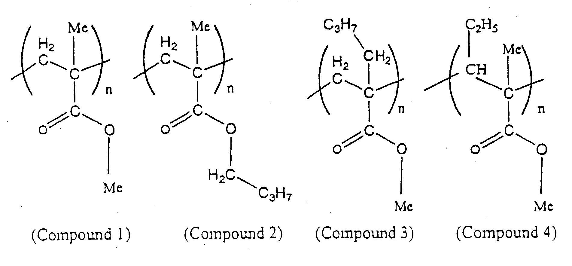

- Table 1 shows calculated results of the line absorption coefficients ( wavelength: 13 nm) of the respective compounds.
40.compounds line absorption coefficients compound 1 4.80 µ-1 compound 2 3.81 µ-1 compound 3 3.84 µ-1 compound 4 4.02 µ-1 compound 5 3.58 µ-1 compound 6 3.66 µ-1 compound 7 3.38 µ-1 - It will be seen from table 1 that, by substituting various alkyl groups for hydrogen atoms, the line absorption coefficients at the wavelength of 13 nm are decreased. In particular, the line absorption coefficient is not larger than 3.80 µ-1 in case of substitution by butyl or hexyl groups.
- A polyvinylphenolic high polymer material (compound 8) was used as a basic high polymer material (pre-existing resist material) and line absorption coefficients of compounds obtained on substituting propyl groups for hydrogen atoms at various positions of the basic high polymer material were found on calculations.
- The structures of a polyvinyl phenol based high polymer material (compound 8) as a basic skeleton and compounds obtained on substitution by propyl groups (compounds 9 to 11) are as shown by the following chemical formula 2: 44.
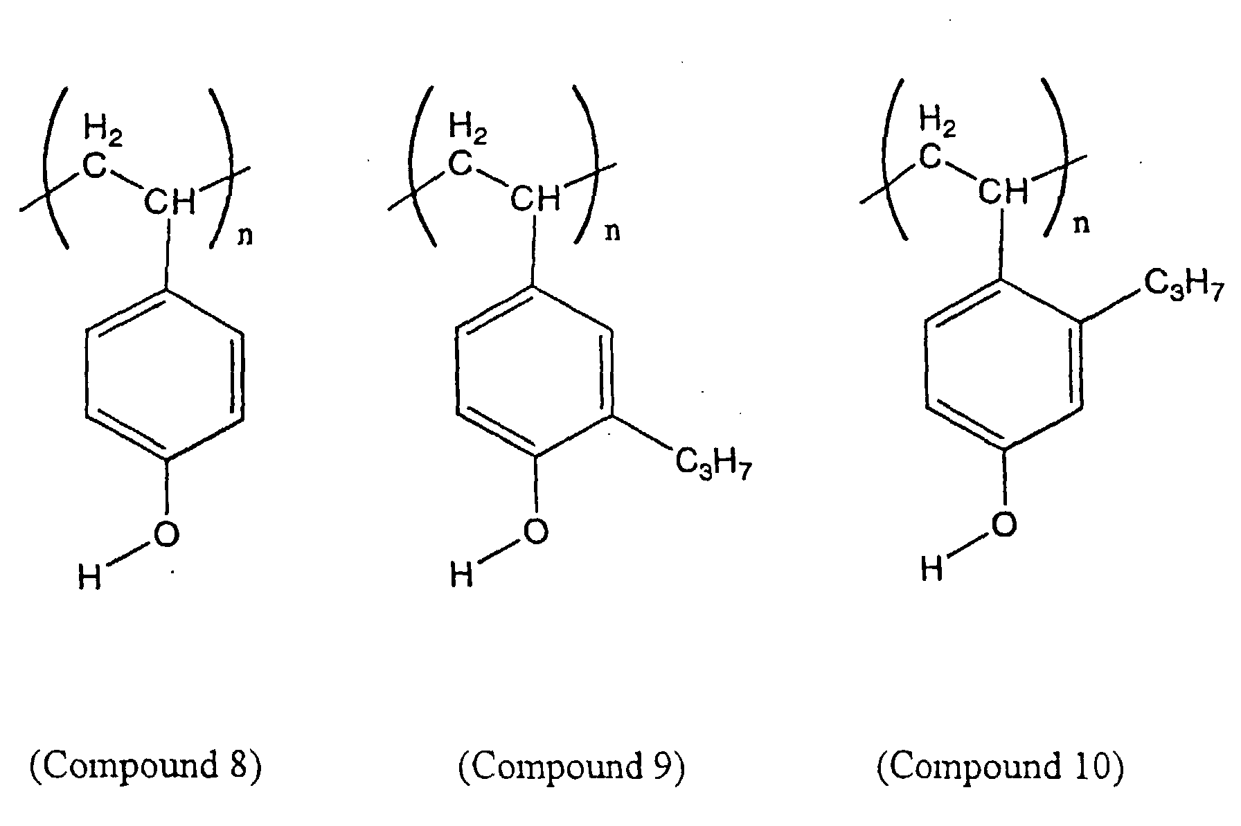

- Table 2 shows calculated results of the line absorption coefficients ( wavelength: 13 nm) of the respective compounds.
Compounds line absorption coefficient Compound 8 3.80 µ-1 Compound 9 3.23 µ-1 Compound 10 3.23 µ-1 Compound 11 3.25 µ-1 - As may be seen from Table 2, the line absorption coefficient at the wavelength of 13 nm is lowered on substituting propyl groups for hydrogen atoms.
- A siloxane based high polymer material (compound 12) was used as a basic high polymer material and its hydrogen atom was replaced by a propyl group to give a compound 13 or by an aminopropyl group to give a compound 14. The structures of the respective compounds are as shown by the following chemical formulas 12 to 14:


- Table 3 shows calculated results of the line absorption coefficients ( wavelength: 13 nm) of the respective compounds.
Compounds line absorption coefficient Compound 12 3.86 µ-1 Compound 13 3.47 µ-1 Compound 14 3.70 µ-1 - As may be seen from Table 3, the line absorption coefficient at the wavelength of 13 nm is lowered on substituting propyl and aminopropyl groups for hydrogen atoms.
- An acrylic high polymer material (compound 15) was used as a basic high polymer material (pre-existing resist material) and its hydrogen atom was replaced by a phenyl group and a naphthalene group to find the line absorption coefficients of the resulting compounds on calculations.
- The structures of the acrylic high polymer material as a basic skeleton (compound 15), a compound 16 obtained on substitution by the phenyl group and a compound 17 obtained on substitution by a naphthalene group are as shown by the following chemical formulas (15) to (17):


- Table 4 shows calculated results of the line absorption coefficients (wavelength: 13 nm) of the respective compounds.
Compounds line absorption coefficient Compound 15 4.80 µ-1 Compound 16 4.06 µ-1 Compound 17 3.96 µ-1 - It will be seen from table 4 that, by substituting phenyl and naphthalene groups for hydrogen atoms, the line absorption coefficients at the wavelength of 13 nm may be decreased.
- A polyvinylphenolic high polymer material (compound 18) was used as a basic high polymer material (pre-existing resist material) and line absorption coefficients of compounds obtained on substituting phenyl-, naphthalene- and methylphenyl groups for hydrogen atoms were found on calculations.
- The structures of a polyvinyl phenol based high polymer material (compound 18) as a basic skeleton and a compound 19 obtained on substitution by a phenyl group, a compound 20 obtained on substitution by a naphthalene group and a compound 21 obtained on substitution by a methylphenyl group, are as shown by the following chemical formulas 18 to 21:
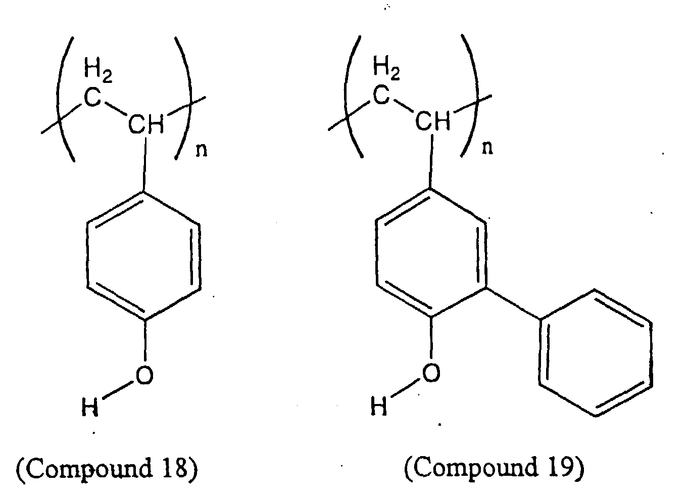

- Table 5 shows calculated results of the line absorption coefficients ( wavelength: 13 nm) of the respective compounds.
Compounds line absorption coefficient Compound 18 3.80 µ-1 Compound 19 3.49 µ-1 Compound 20 3.50 µ-1 Compound 21 3.35 µ-1 - As may be seen from Table 5, the line absorption coefficient at the wavelength of 13 nm is lowered on substituting propyl groups for hydrogen atoms.
- A siloxane based high polymer material (compound 22) was used as a basic high polymer material (pre-existing resist material) and its hydrogen atom was replaced by a phenyl group or a naphthalene group to give compounds 23, 24, respectively, and the line absorption coefficients of these compounds were calculated.
- The structures of the siloxane-based high polymer material (compound 22) as a basic structure, a compound obtained on substituting a phenyl group (compound 23) and a compound obtained on substituting a naphthalene group (compound 24) are as shown by the following chemical formulas (22) to (24):


- Table 6 shows calculated results of the line absorption coefficients ( wavelength: 13 nm) of the respective compounds.
Compounds line absorption coefficient Compound 22 3.86 µ-1 Compound 23 3.67 µ-1 Compound 24 3.65 µ-1 - It will be seen from table 4 that, by substituting phenyl and naphthalene groups for hydrogen atoms, the line absorption coefficients at the wavelength of 13 nm may be decreased.
- Of the high polymer material composed of usual carbon, hydrogen and oxygen (and occasionally nitrogen), a high polymer material containing fluorine atoms, a high polymer material containing silicon (Si) and a high polymer material containing an aromatic ring, the distribution of the line absorption coefficient and the density was mapped. The results are shown in Fig.1.
- With a high polymer material into which silicon (Si) with a low line absorption coefficient is introduced, the line absorption coefficient is decreased only slightly as compared to a usual high polymer material. However, with a high polymer material into which an aromatic ring has been introduced, the line absorption coefficient is lowered to a larger extent.
- Of course, with a high polymer material into which fluorine atoms with a larger line absorption coefficient are introduced, the line absorption coefficient is larger than in the usual high polymer material.
- Thus, it may be seen that, with any high polymer materials, the line absorption coefficient at the wavelength of 13 nm is lowered by substituting an alkyl group or an aromatic ring, such as phenyl or naphthalene groups, for a hydrogen atom of the high polymer material. That is, by substitution by alkyl groups or aromatic rings, it is possible to realize a material superior in transparency for use as a resist material.
- In the foregoing description, acrylic high molecular materials, polyvinyl phenolic high molecular materials and siloxane-based high molecular materials are used as illustrative of the high molecular materials. These compounds are, however, merely illustrative such that any other suitable materials, such as other vinyl-based high molecular materials, polyimide based high molecular materials or the fluorine-based high molecular materials may also be used.
- The substituents are also not limited to those shown in the Examples since any suitable alkyl groups, such as methyl, pentyl or hexyl substituents, may also be used. Similarly, any suitable aromatic rings may be used as substituents, such as phenyl-, naphthalene-, anthracene-, biphenyl- or triphenyl substituents, may be used as aromatic ring substituents.
Claims (5)
- A light exposure method in which a resist layer is exposed selectively to X-rays, vacuum ultraviolet rays, extreme ultraviolet rays or soft X-rays to pattern the resist layer to a pre-set shape;
wherein
as a high molecular material of the resist layer, a high molecular material obtained by replacing at least a portion of hydrogen atoms of a pre-existing resist material by a substituent containing an alkyl group and/or a substituent containing an aromatic ring. - The light exposure method according to claim 1 wherein the line absorption coefficient in an X-ray wavelength range of the high molecular material constituting said resist layer is 3.80 µ-1 or less.
- The light exposure method according to claim 1 wherein ultraviolet rays are used as said X-rays.
- The light exposure method according to claim 3 wherein the wavelength of said ultraviolet rays is 7 to 16 nm.
- The light exposure method according to claim 1 wherein said light exposure is by size-reducing projection employing a size-reducing projection optical system.
Applications Claiming Priority (2)
| Application Number | Priority Date | Filing Date | Title |
|---|---|---|---|
| JP30771899 | 1999-10-28 | ||
| JP30771899A JP2001125268A (en) | 1999-10-28 | 1999-10-28 | Exposure method |
Publications (1)
| Publication Number | Publication Date |
|---|---|
| EP1096321A1 true EP1096321A1 (en) | 2001-05-02 |
Family
ID=17972421
Family Applications (1)
| Application Number | Title | Priority Date | Filing Date |
|---|---|---|---|
| EP00402998A Withdrawn EP1096321A1 (en) | 1999-10-28 | 2000-10-27 | Light exposure method |
Country Status (4)
| Country | Link |
|---|---|
| US (1) | US6613497B1 (en) |
| EP (1) | EP1096321A1 (en) |
| JP (1) | JP2001125268A (en) |
| KR (1) | KR100735857B1 (en) |
Families Citing this family (1)
| Publication number | Priority date | Publication date | Assignee | Title |
|---|---|---|---|---|
| JP2003186194A (en) * | 2001-12-20 | 2003-07-03 | Sony Corp | Resist material and exposure method |
Citations (5)
| Publication number | Priority date | Publication date | Assignee | Title |
|---|---|---|---|---|
| JPS52146218A (en) * | 1976-05-31 | 1977-12-05 | Toshiba Corp | Positive type radiation sensitive material |
| DD146220A1 (en) * | 1979-09-14 | 1981-01-28 | Lorkowski Hans Joachim | METHOD FOR PRODUCING HOMOGENEOUS POLYMETHYL METHACRYLATE LAYERS ON SUBSTRATE SURFACES |
| JPS61148445A (en) * | 1984-12-24 | 1986-07-07 | Tokyo Ohka Kogyo Co Ltd | Radiation sensitive negative type resist material |
| US4634645A (en) * | 1984-04-13 | 1987-01-06 | Nippon Telegraph And Telephone Corporation | Method of forming resist micropattern |
| DD277773A1 (en) * | 1988-12-02 | 1990-04-11 | Akad Wissenschaften Ddr | WAESSER-ALKALISCH DEVELOPABLE POSITIVE RESISTANT |
Family Cites Families (18)
| Publication number | Priority date | Publication date | Assignee | Title |
|---|---|---|---|---|
| DE146220C (en) | ||||
| DE277773C (en) | ||||
| FR2583534B1 (en) * | 1985-06-18 | 1990-06-22 | Labo Electronique Physique | COMPOSITION FOR OBTAINING A HIGH RESOLUTION PHOTOSENSITIVE RESIN, DEVELOPABLE BY PLASMA AND PHOTOLITHOGRAPHIC METHOD USING THE SAME. |
| JPH0425530A (en) * | 1990-05-21 | 1992-01-29 | Nippon Telegr & Teleph Corp <Ntt> | Siloxane polymer and resist composition |
| JP3008594B2 (en) * | 1990-08-31 | 2000-02-14 | 和光純薬工業株式会社 | New resist material and pattern forming method |
| US5352899A (en) * | 1992-08-18 | 1994-10-04 | Ruxam, Inc. | Method and apparatus for fabricating a device/circuit pattern by a converging atomic beam |
| JP3116751B2 (en) * | 1993-12-03 | 2000-12-11 | ジェイエスアール株式会社 | Radiation-sensitive resin composition |
| US5510230A (en) * | 1994-10-20 | 1996-04-23 | At&T Corp. | Device fabrication using DUV/EUV pattern delineation |
| JPH0971658A (en) * | 1995-09-06 | 1997-03-18 | Hokushin Ind Inc | New compound containing silicon, its production and resist material |
| JP3890358B2 (en) * | 1996-03-11 | 2007-03-07 | 富士フイルム株式会社 | Positive photosensitive resin composition and pattern forming method |
| JPH09258450A (en) * | 1996-03-22 | 1997-10-03 | Hitachi Ltd | Exposure method and semiconductor manufacturing method |
| KR100234143B1 (en) * | 1996-06-07 | 1999-12-15 | 미야즈 쥰이치로 | Resist material and fabrication method thereof |
| JP3778620B2 (en) * | 1996-07-15 | 2006-05-24 | 岡本化学工業株式会社 | Photosensitive composition |
| JPH1039501A (en) * | 1996-07-19 | 1998-02-13 | Sekisui Finechem Co Ltd | Colored photosensitive resin composition and color filter |
| JP3724890B2 (en) * | 1996-09-05 | 2005-12-07 | 富士通株式会社 | Chemically amplified resist composition and method for forming resist pattern |
| JPH10319594A (en) * | 1997-05-21 | 1998-12-04 | Fuji Photo Film Co Ltd | Positive photoresist composition for far ultraviolet ray exposure |
| JP3676918B2 (en) * | 1997-10-09 | 2005-07-27 | 富士通株式会社 | Resist material and resist pattern forming method |
| JPH11286549A (en) * | 1998-02-05 | 1999-10-19 | Canon Inc | Photosensitive resin, resist using the photosensitive resin, exposure apparatus and exposure method using the resist, and semiconductor device obtained by the exposure method |
-
1999
- 1999-10-28 JP JP30771899A patent/JP2001125268A/en active Pending
-
2000
- 2000-10-27 US US09/697,736 patent/US6613497B1/en not_active Expired - Fee Related
- 2000-10-27 KR KR1020000063523A patent/KR100735857B1/en not_active Expired - Fee Related
- 2000-10-27 EP EP00402998A patent/EP1096321A1/en not_active Withdrawn
Patent Citations (5)
| Publication number | Priority date | Publication date | Assignee | Title |
|---|---|---|---|---|
| JPS52146218A (en) * | 1976-05-31 | 1977-12-05 | Toshiba Corp | Positive type radiation sensitive material |
| DD146220A1 (en) * | 1979-09-14 | 1981-01-28 | Lorkowski Hans Joachim | METHOD FOR PRODUCING HOMOGENEOUS POLYMETHYL METHACRYLATE LAYERS ON SUBSTRATE SURFACES |
| US4634645A (en) * | 1984-04-13 | 1987-01-06 | Nippon Telegraph And Telephone Corporation | Method of forming resist micropattern |
| JPS61148445A (en) * | 1984-12-24 | 1986-07-07 | Tokyo Ohka Kogyo Co Ltd | Radiation sensitive negative type resist material |
| DD277773A1 (en) * | 1988-12-02 | 1990-04-11 | Akad Wissenschaften Ddr | WAESSER-ALKALISCH DEVELOPABLE POSITIVE RESISTANT |
Non-Patent Citations (4)
| Title |
|---|
| DATABASE WPI Section Ch Week 197804, Derwent World Patents Index; Class A89, AN 1978-07005A, XP002158502 * |
| DATABASE WPI Section Ch Week 198116, Derwent World Patents Index; Class A14, AN 1981-27344D, XP002158501 * |
| DATABASE WPI Section Ch Week 198633, Derwent World Patents Index; Class A89, AN 1986-216249, XP002158500 * |
| DATABASE WPI Section Ch Week 199038, Derwent World Patents Index; Class A14, AN 1990-283191, XP002158499 * |
Also Published As
| Publication number | Publication date |
|---|---|
| US6613497B1 (en) | 2003-09-02 |
| KR20010040199A (en) | 2001-05-15 |
| JP2001125268A (en) | 2001-05-11 |
| KR100735857B1 (en) | 2007-07-04 |
Similar Documents
| Publication | Publication Date | Title |
|---|---|---|
| Yildirim et al. | Improvements in resist performance towards EUV HVM | |
| TW518661B (en) | Electron beam exposure method having good linearity with respect to producing fine patterns | |
| De Simone et al. | 28nm pitch single exposure patterning readiness by metal oxide resist on 0.33 NA EUV lithography | |
| US5338818A (en) | Silicon containing positive resist for DUV lithography | |
| Medeiros et al. | Recent progress in electron-beam resists for advanced mask-making | |
| KR20100027995A (en) | Patterning process | |
| Nakamura et al. | Contact hole formation by multiple exposure technique in ultralow k1 lithography | |
| JP4551704B2 (en) | Protective film forming composition for immersion exposure and pattern forming method using the same | |
| De Simone et al. | Progresses and challenges of EUV lithography materials | |
| TWI278013B (en) | Self-aligned pattern formation using dual wavelengths | |
| Carbaugh et al. | Combination photo and electron beam lithography with polymethyl methacrylate (PMMA) resist | |
| EP0745633B1 (en) | Si containing high molecular compound and photosensitive resin composition | |
| KR101685903B1 (en) | Method for forming fine pattern in semiconductor device | |
| EP1096321A1 (en) | Light exposure method | |
| Popescu et al. | Component optimisation in the multi-trigger resist | |
| Sahoo et al. | Progress in deep-UV photoresists | |
| Grube et al. | Medusa 82—Hydrogen silsesquioxane based high sensitivity negative-tone resist with long shelf-life and grayscale lithography capability | |
| Kundu et al. | Substantial dose reduction using dry deposited underlayer for EUV lithography while maintaining roughness and minimizing defects | |
| US20030128802A1 (en) | Resist material and exposure method | |
| Takahata et al. | Study of MEEF improvement with low-n absorber EUVL mask | |
| Han et al. | Underlayer material design for extreme ultraviolet negative-tone development photolithography process by controlling photoresist-underlayer intermixing | |
| Shirotori et al. | Development on main chain scission resists for high-NA EUV lithography | |
| US6677108B2 (en) | Method for light exposure | |
| JP2001222109A (en) | Exposure method | |
| Takahata et al. | Study of mask error enhancement factor improvement with low-n absorber extreme ultraviolet lithography mask |
Legal Events
| Date | Code | Title | Description |
|---|---|---|---|
| PUAI | Public reference made under article 153(3) epc to a published international application that has entered the european phase |
Free format text: ORIGINAL CODE: 0009012 |
|
| AK | Designated contracting states |
Kind code of ref document: A1 Designated state(s): DE FR GB |
|
| AX | Request for extension of the european patent |
Free format text: AL;LT;LV;MK;RO;SI |
|
| 17P | Request for examination filed |
Effective date: 20011030 |
|
| AKX | Designation fees paid |
Free format text: AT BE CH LI |
|
| REG | Reference to a national code |
Ref country code: DE Ref legal event code: 8566 |
|
| RBV | Designated contracting states (corrected) |
Designated state(s): DE FR GB |
|
| RBV | Designated contracting states (corrected) |
Designated state(s): DE FR GB |
|
| 17Q | First examination report despatched |
Effective date: 20090220 |
|
| STAA | Information on the status of an ep patent application or granted ep patent |
Free format text: STATUS: THE APPLICATION IS DEEMED TO BE WITHDRAWN |
|
| 18D | Application deemed to be withdrawn |
Effective date: 20090703 |