EP1094547A2 - Electrical connector with strain relief - Google Patents
Electrical connector with strain relief Download PDFInfo
- Publication number
- EP1094547A2 EP1094547A2 EP00122278A EP00122278A EP1094547A2 EP 1094547 A2 EP1094547 A2 EP 1094547A2 EP 00122278 A EP00122278 A EP 00122278A EP 00122278 A EP00122278 A EP 00122278A EP 1094547 A2 EP1094547 A2 EP 1094547A2
- Authority
- EP
- European Patent Office
- Prior art keywords
- connector
- substrate
- electrical connector
- recited
- housing
- Prior art date
- Legal status (The legal status is an assumption and is not a legal conclusion. Google has not performed a legal analysis and makes no representation as to the accuracy of the status listed.)
- Granted
Links
Images




Classifications
-
- H—ELECTRICITY
- H05—ELECTRIC TECHNIQUES NOT OTHERWISE PROVIDED FOR
- H05K—PRINTED CIRCUITS; CASINGS OR CONSTRUCTIONAL DETAILS OF ELECTRIC APPARATUS; MANUFACTURE OF ASSEMBLAGES OF ELECTRICAL COMPONENTS
- H05K3/00—Apparatus or processes for manufacturing printed circuits
- H05K3/30—Assembling printed circuits with electric components, e.g. with resistors
- H05K3/303—Assembling printed circuits with electric components, e.g. with resistors with surface mounted components
-
- H—ELECTRICITY
- H01—ELECTRIC ELEMENTS
- H01R—ELECTRICALLY-CONDUCTIVE CONNECTIONS; STRUCTURAL ASSOCIATIONS OF A PLURALITY OF MUTUALLY-INSULATED ELECTRICAL CONNECTING ELEMENTS; COUPLING DEVICES; CURRENT COLLECTORS
- H01R12/00—Structural associations of a plurality of mutually-insulated electrical connecting elements, specially adapted for printed circuits, e.g. printed circuit boards [PCB], flat or ribbon cables, or like generally planar structures, e.g. terminal strips, terminal blocks; Coupling devices specially adapted for printed circuits, flat or ribbon cables, or like generally planar structures; Terminals specially adapted for contact with, or insertion into, printed circuits, flat or ribbon cables, or like generally planar structures
- H01R12/70—Coupling devices
- H01R12/7005—Guiding, mounting, polarizing or locking means; Extractors
- H01R12/7011—Locking or fixing a connector to a PCB
-
- H—ELECTRICITY
- H01—ELECTRIC ELEMENTS
- H01R—ELECTRICALLY-CONDUCTIVE CONNECTIONS; STRUCTURAL ASSOCIATIONS OF A PLURALITY OF MUTUALLY-INSULATED ELECTRICAL CONNECTING ELEMENTS; COUPLING DEVICES; CURRENT COLLECTORS
- H01R12/00—Structural associations of a plurality of mutually-insulated electrical connecting elements, specially adapted for printed circuits, e.g. printed circuit boards [PCB], flat or ribbon cables, or like generally planar structures, e.g. terminal strips, terminal blocks; Coupling devices specially adapted for printed circuits, flat or ribbon cables, or like generally planar structures; Terminals specially adapted for contact with, or insertion into, printed circuits, flat or ribbon cables, or like generally planar structures
- H01R12/70—Coupling devices
- H01R12/7005—Guiding, mounting, polarizing or locking means; Extractors
- H01R12/7011—Locking or fixing a connector to a PCB
- H01R12/7052—Locking or fixing a connector to a PCB characterised by the locating members
-
- H—ELECTRICITY
- H01—ELECTRIC ELEMENTS
- H01R—ELECTRICALLY-CONDUCTIVE CONNECTIONS; STRUCTURAL ASSOCIATIONS OF A PLURALITY OF MUTUALLY-INSULATED ELECTRICAL CONNECTING ELEMENTS; COUPLING DEVICES; CURRENT COLLECTORS
- H01R13/00—Details of coupling devices of the kinds covered by groups H01R12/70 or H01R24/00 - H01R33/00
- H01R13/58—Means for relieving strain on wire connection, e.g. cord grip, for avoiding loosening of connections between wires and terminals within a coupling device terminating a cable
-
- H—ELECTRICITY
- H01—ELECTRIC ELEMENTS
- H01R—ELECTRICALLY-CONDUCTIVE CONNECTIONS; STRUCTURAL ASSOCIATIONS OF A PLURALITY OF MUTUALLY-INSULATED ELECTRICAL CONNECTING ELEMENTS; COUPLING DEVICES; CURRENT COLLECTORS
- H01R43/00—Apparatus or processes specially adapted for manufacturing, assembling, maintaining, or repairing of line connectors or current collectors or for joining electric conductors
- H01R43/02—Apparatus or processes specially adapted for manufacturing, assembling, maintaining, or repairing of line connectors or current collectors or for joining electric conductors for soldered or welded connections
- H01R43/0256—Apparatus or processes specially adapted for manufacturing, assembling, maintaining, or repairing of line connectors or current collectors or for joining electric conductors for soldered or welded connections for soldering or welding connectors to a printed circuit board
-
- H—ELECTRICITY
- H01—ELECTRIC ELEMENTS
- H01R—ELECTRICALLY-CONDUCTIVE CONNECTIONS; STRUCTURAL ASSOCIATIONS OF A PLURALITY OF MUTUALLY-INSULATED ELECTRICAL CONNECTING ELEMENTS; COUPLING DEVICES; CURRENT COLLECTORS
- H01R12/00—Structural associations of a plurality of mutually-insulated electrical connecting elements, specially adapted for printed circuits, e.g. printed circuit boards [PCB], flat or ribbon cables, or like generally planar structures, e.g. terminal strips, terminal blocks; Coupling devices specially adapted for printed circuits, flat or ribbon cables, or like generally planar structures; Terminals specially adapted for contact with, or insertion into, printed circuits, flat or ribbon cables, or like generally planar structures
- H01R12/50—Fixed connections
- H01R12/51—Fixed connections for rigid printed circuits or like structures
- H01R12/55—Fixed connections for rigid printed circuits or like structures characterised by the terminals
- H01R12/57—Fixed connections for rigid printed circuits or like structures characterised by the terminals surface mounting terminals
-
- H—ELECTRICITY
- H01—ELECTRIC ELEMENTS
- H01R—ELECTRICALLY-CONDUCTIVE CONNECTIONS; STRUCTURAL ASSOCIATIONS OF A PLURALITY OF MUTUALLY-INSULATED ELECTRICAL CONNECTING ELEMENTS; COUPLING DEVICES; CURRENT COLLECTORS
- H01R12/00—Structural associations of a plurality of mutually-insulated electrical connecting elements, specially adapted for printed circuits, e.g. printed circuit boards [PCB], flat or ribbon cables, or like generally planar structures, e.g. terminal strips, terminal blocks; Coupling devices specially adapted for printed circuits, flat or ribbon cables, or like generally planar structures; Terminals specially adapted for contact with, or insertion into, printed circuits, flat or ribbon cables, or like generally planar structures
- H01R12/70—Coupling devices
- H01R12/7005—Guiding, mounting, polarizing or locking means; Extractors
-
- H—ELECTRICITY
- H01—ELECTRIC ELEMENTS
- H01R—ELECTRICALLY-CONDUCTIVE CONNECTIONS; STRUCTURAL ASSOCIATIONS OF A PLURALITY OF MUTUALLY-INSULATED ELECTRICAL CONNECTING ELEMENTS; COUPLING DEVICES; CURRENT COLLECTORS
- H01R12/00—Structural associations of a plurality of mutually-insulated electrical connecting elements, specially adapted for printed circuits, e.g. printed circuit boards [PCB], flat or ribbon cables, or like generally planar structures, e.g. terminal strips, terminal blocks; Coupling devices specially adapted for printed circuits, flat or ribbon cables, or like generally planar structures; Terminals specially adapted for contact with, or insertion into, printed circuits, flat or ribbon cables, or like generally planar structures
- H01R12/70—Coupling devices
- H01R12/7005—Guiding, mounting, polarizing or locking means; Extractors
- H01R12/7011—Locking or fixing a connector to a PCB
- H01R12/707—Soldering or welding
-
- H—ELECTRICITY
- H01—ELECTRIC ELEMENTS
- H01R—ELECTRICALLY-CONDUCTIVE CONNECTIONS; STRUCTURAL ASSOCIATIONS OF A PLURALITY OF MUTUALLY-INSULATED ELECTRICAL CONNECTING ELEMENTS; COUPLING DEVICES; CURRENT COLLECTORS
- H01R12/00—Structural associations of a plurality of mutually-insulated electrical connecting elements, specially adapted for printed circuits, e.g. printed circuit boards [PCB], flat or ribbon cables, or like generally planar structures, e.g. terminal strips, terminal blocks; Coupling devices specially adapted for printed circuits, flat or ribbon cables, or like generally planar structures; Terminals specially adapted for contact with, or insertion into, printed circuits, flat or ribbon cables, or like generally planar structures
- H01R12/70—Coupling devices
- H01R12/71—Coupling devices for rigid printing circuits or like structures
- H01R12/712—Coupling devices for rigid printing circuits or like structures co-operating with the surface of the printed circuit or with a coupling device exclusively provided on the surface of the printed circuit
- H01R12/716—Coupling device provided on the PCB
-
- H—ELECTRICITY
- H01—ELECTRIC ELEMENTS
- H01R—ELECTRICALLY-CONDUCTIVE CONNECTIONS; STRUCTURAL ASSOCIATIONS OF A PLURALITY OF MUTUALLY-INSULATED ELECTRICAL CONNECTING ELEMENTS; COUPLING DEVICES; CURRENT COLLECTORS
- H01R13/00—Details of coupling devices of the kinds covered by groups H01R12/70 or H01R24/00 - H01R33/00
- H01R13/648—Protective earth or shield arrangements on coupling devices, e.g. anti-static shielding
- H01R13/658—High frequency shielding arrangements, e.g. against EMI [Electro-Magnetic Interference] or EMP [Electro-Magnetic Pulse]
- H01R13/6581—Shield structure
- H01R13/6585—Shielding material individually surrounding or interposed between mutually spaced contacts
-
- H—ELECTRICITY
- H01—ELECTRIC ELEMENTS
- H01R—ELECTRICALLY-CONDUCTIVE CONNECTIONS; STRUCTURAL ASSOCIATIONS OF A PLURALITY OF MUTUALLY-INSULATED ELECTRICAL CONNECTING ELEMENTS; COUPLING DEVICES; CURRENT COLLECTORS
- H01R4/00—Electrically-conductive connections between two or more conductive members in direct contact, i.e. touching one another; Means for effecting or maintaining such contact; Electrically-conductive connections having two or more spaced connecting locations for conductors and using contact members penetrating insulation
- H01R4/02—Soldered or welded connections
- H01R4/028—Soldered or welded connections comprising means for preventing flowing or wicking of solder or flux in parts not desired
-
- H—ELECTRICITY
- H05—ELECTRIC TECHNIQUES NOT OTHERWISE PROVIDED FOR
- H05K—PRINTED CIRCUITS; CASINGS OR CONSTRUCTIONAL DETAILS OF ELECTRIC APPARATUS; MANUFACTURE OF ASSEMBLAGES OF ELECTRICAL COMPONENTS
- H05K2201/00—Indexing scheme relating to printed circuits covered by H05K1/00
- H05K2201/10—Details of components or other objects attached to or integrated in a printed circuit board
- H05K2201/10431—Details of mounted components
- H05K2201/10568—Integral adaptations of a component or an auxiliary PCB for mounting, e.g. integral spacer element
-
- H—ELECTRICITY
- H05—ELECTRIC TECHNIQUES NOT OTHERWISE PROVIDED FOR
- H05K—PRINTED CIRCUITS; CASINGS OR CONSTRUCTIONAL DETAILS OF ELECTRIC APPARATUS; MANUFACTURE OF ASSEMBLAGES OF ELECTRICAL COMPONENTS
- H05K2203/00—Indexing scheme relating to apparatus or processes for manufacturing printed circuits covered by H05K3/00
- H05K2203/15—Position of the PCB during processing
- H05K2203/159—Using gravitational force; Processing against the gravity direction; Using centrifugal force
-
- H—ELECTRICITY
- H05—ELECTRIC TECHNIQUES NOT OTHERWISE PROVIDED FOR
- H05K—PRINTED CIRCUITS; CASINGS OR CONSTRUCTIONAL DETAILS OF ELECTRIC APPARATUS; MANUFACTURE OF ASSEMBLAGES OF ELECTRICAL COMPONENTS
- H05K3/00—Apparatus or processes for manufacturing printed circuits
- H05K3/30—Assembling printed circuits with electric components, e.g. with resistors
- H05K3/32—Assembling printed circuits with electric components, e.g. with resistors electrically connecting electric components or wires to printed circuits
- H05K3/34—Assembling printed circuits with electric components, e.g. with resistors electrically connecting electric components or wires to printed circuits by soldering
- H05K3/341—Surface mounted components
- H05K3/3421—Leaded components
-
- Y—GENERAL TAGGING OF NEW TECHNOLOGICAL DEVELOPMENTS; GENERAL TAGGING OF CROSS-SECTIONAL TECHNOLOGIES SPANNING OVER SEVERAL SECTIONS OF THE IPC; TECHNICAL SUBJECTS COVERED BY FORMER USPC CROSS-REFERENCE ART COLLECTIONS [XRACs] AND DIGESTS
- Y02—TECHNOLOGIES OR APPLICATIONS FOR MITIGATION OR ADAPTATION AGAINST CLIMATE CHANGE
- Y02P—CLIMATE CHANGE MITIGATION TECHNOLOGIES IN THE PRODUCTION OR PROCESSING OF GOODS
- Y02P70/00—Climate change mitigation technologies in the production process for final industrial or consumer products
- Y02P70/50—Manufacturing or production processes characterised by the final manufactured product
Definitions
- the invention relates to electrical connectors. More specifically, the invention relates to electrical connectors with strain relief features.
- SMT connectors provide numerous benefits over earlier connectors, such as simplified manufacturing and lower costs.
- SMT may raise other issues.
- One concern involves the ability of the solder joint between the contact and the underlying substrate to absorb forces caused by, for example, shipping, handling, mating and thermal cycling. Should one solder joint become unusable as a result of damage from any of these events, the entire connector adversely may be affected.
- Ball grid array (BGA) technology is one type of SMT.
- an electrical connector using a BGA has a housing with a contact therein.
- a fusible element typically a solder ball, secures to each contact.
- the solder balls serve as the primary connection between the contact and the surface of the substrate.
- a reflow process fuses the solder ball to the substrate.
- a beneficial "self-centering" feature of the BGA technology occurs. Specifically, as the solder reflows, the surface tension of the solder helps to align the connector properly with the conductive pads on the underlying substrate.
- an electrical connector mountable to a substrate comprises a housing, and a surface mount contact and hold down both secured to the housing.
- the hold down may be a surface mount hold down.
- the connector may further comprise a shield generally surrounding the housing, wherein the hold down is part of the shield.
- the surface mount contact may include a fusible element in the form of a solder ball.
- the surface mount contacts may form a matrix array.
- the electrical connector may be constructed such that it remains substantially parallel when mounted to the substrate.
- the electrical connector may include a standoff secured to the housing, wherein the standoff is adapted to retain the housing a distance from a surface of the substrate. The standoff may be a part of the shield.
- a ball grid array connector comprising a housing, a plurality of contacts within the housing, a plurality of fusible elements secured to the contacts for mounting the connector to a substrate, and a hold down secured to the housing.
- the hold down may be a surface mount hold down.
- the ball grid array connector may further comprise a shield generally surrounding the housing, wherein the hold down is part of the shield.
- the ball grid array connector may include a standoff extending from the housing and adapted to retain the housing a distance from a surface of the substrate. The standoff may be a part of the shield.
- the ball grid array connector may be constructed such that it remains substantially parallel when mounted to the substrate.
- the method comprises providing a substrate and an electrical connector having a contact and a hold down, and securing the contact and the hold down to the substrate.
- the contact may be secured to a surface of the substrate.
- the contact may be secured before the hold down is secured, using a soldering technique, for example, to permit the connector to self-center on the substrate.
- the electrical connector may include a shield that is secured to the substrate.
- the method may further comprise constructing the electrical connector such that it remains substantially parallel when mounted to the substrate. Also, the method may comprise balancing the electrical connector on the substrate such that the electrical connector remains substantially parallel to the substrate during they are attached.
- the electrical connector may be a ball grid array connector.
- a method of securing an electrical connector to a substrate comprises providing a substrate and an electrical connector having a contact and a hold down, and mounting the contact to the substrate.
- the method further comprises balancing the electrical connector on the substrate such that the electrical connector remains substantially parallel to the substrate during the forming of the first and second solder joints.
- Such balancing may be accomplished by removing material from and/or adding material to the electrical connector.
- the balancing may be accomplished by exerting an external force on the electrical connector and/or the substrate during the forming of the first and second solder joints.
- an improved array connector having a plurality of fusible elements that are able to support a nominal mass without an undesired flattening of the fusible elements.
- the nominal mass is less than a mass of the connector.
- the improvement comprises a feature on the connector that prevents the undesired flattening of the fusible elements.
- the feature may comprise a standoff.
- the feature may comprise an area of material removed from a housing of the connector.
- an improved electrical connector mountable to a substrate, having an array of fusible elements, and exhibiting an unbalance relative to the fusible elements.
- the improvement comprises a feature on the connector that prevents the unbalance from causing an undesired skewing of the connector when mounting the connector to the substrate.
- the feature may comprise a standoff.
- the feature may comprise an area of material removed from a housing of the connector.
- each of the alternative embodiments described herein relates to surface mounted electrical connectors having strain relief features.
- fusible elements such as solder balls
- BGA ball grid array
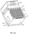
- FIGS 1, 2A and 2B display electrical connector 100.
- Receptacle backplane connector 100 uses many of the features described in U.S. Patent No. 6,116,926, herein incorporated by reference. Because a detailed discussion of the interior features of connector 100 are unnecessary for an understanding of the invention, only a brief summary of the interior features follows.
- Connector 100 is modular, formed by a series of sub-assemblies 101.
- Rear insulative housing 103 and front insulative housing 105 can latch together and surround sub-assemblies 101 to form connector 100.
- Front housing 105 includes lead-in openings 107 that accept conductive pins from a mating connector (as shown in Figures 3, 4A and 4B). Openings 107 form a differential pair arrangement, with two rows of openings 107s that receive signal pins flanked by a row of openings 107g that receive ground pins.
- An external shield 109 can surround at least rear housing 103.
- Shield 109 is preferably made from a suitable solderable material such as a copper alloy.
- Shield 109 preferably extends along at least three sides of connector 100, the rear wall and the two side walls.
- shield 109 also includes bent tabs 111 that extend along portions of the bottom wall of connector 100 ( i.e ., the wall that faces substrate S).
- Sub-assemblies 101 contain the ground contacts 113 and signal contacts 115 of connector 100. Ground and signal contacts 113, 115 mate with corresponding ground and signal pins of the mating connector. Differently than shown in U.S. Parent No. 6,116,926, the signal and ground contacts of connector 100 surface mount to a substrate S, typically a multi-layer circuit board (MLB).
- MLB multi-layer circuit board
- the preferred method of surface mounting connector 100 utilizes BGA technology.
- International Publication number WO 98/15991 International Patent Application number PCT/US97/18354
- PCT/US97/18354 describes various connectors and methods of making connectors using BGA technology.
- Fusible elements 117 secure to a distal region of contacts 113, 115.
- fusible elements 117 are solder balls fused to contacts 113, 115 during a reflow process.
- Contacts 113, 115 can have a tab at a distal end region to which solder balls 117 fuse.
- any other manner of securing fusible elements 117 to contacts 113, 115 could be used, such as placing the distal ends of contacts 113, 115 within a pocket (in Figure 4B) of the connector housing.
- substrate S has an array of conductive pads C connected to suitable traces (not shown) to transmit signals or for grounding purposes, for example.
- Pads C correspond to the array of fusible elements 117 secured to contacts 113, 115 on connector 100.
- a reflow process typically subsequent to the reflow process that fused solder balls 117 to contacts 113, 115, fuses solder balls 117 to pads C.
- pads C have solder paste (not shown) thereon to accept and to temporarily secure solder balls 117 to substrate S.
- solder paste typically a squeegee drawn across a stencil (not shown) placed on substrate S provides suitable amounts of solder paste at desired locations. The reflow process fuses solder ball 117 to pad C on substrate S, thus creating an electrical path between contacts 113, 115 and substrate S.
- substrate S includes additional conductive pads H at suitable locations, such as surrounding conductive pads C. Conducuve pads H preferably match the locations of tabs 111 of external shield 109. In this way, tabs 111 act as hold downs to secure housing 109 to the surface of substrate S.
- the reflow process used to secure solder balls 117 to substrate S preferably also secures conductive shield 109 to substrate S.
- conductive pads H receive solder paste during the squeegee operation.
- the reflow process fuses shield 109 to substrate S.
- Securing conductive shield 109 to substrate S serves as the strain relief for connector 100. Because shield 109 surface mounts to substrate S, the strain relief feature of connector 100 does not interfere with the self-centering characteristic of fusible elements 117 during reflow.
- the invention may protect the solder balls from being flattened during reflow because of the weight of the connector. Such flattening may cause unwanted bridging between adjacent solder balls.
- the connector may include a standoff.
- the standoff limits the ability of the connector to approach the substrate when the solder balls liquefy. In other words, the standoff prevents the solder balls from being flattened by the weight of the connector and from possibly bridging with adjacent solder balls.
- the standoffs may be made from any suitable material.
- shield 109 acts as the standoff. Shield 109 allows only a portion of solder balls 117 to extend a distance d beyond shield 109.
- Distance d is selected so as to limit the flattening of solder balls during the reflow process.
- the stand-off could allow up to 40 percent, preferably 30 percent, flattening of the solder balls.
- Distance d also is selected to limit the bridging of adjacent solder balls during the reflow process. In this way, shield 209 acts like a standoff by preventing connector 100 from skewing on the PCB during reflow.
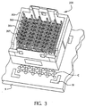
- FIGS 3, 4A and 4B display electrical connector 200.
- Backplane header connector 200 preferably mates with backplane receptacle connector 100.
- connectors 100, 200 are used in a backplane system, for example, to connect a daughtercard to a motherboard.
- Connector 200 uses many of the features described in U.S. Patent Application serial number 09/302,027, herein incorporated by reference. Because a detailed discussion of certain features of connector 200 are unnecessary for an understanding of the invention, only a brief summary of these features follows.
- Connector 200 includes an insulative housing 201 with apertures therethrough that accept signal pins 203, ground pins 205 and ground shields 207.
- Signal and ground pins 203, 205 extend from housing 201 and correspond to the arrangement of lead-in apertures 107 in connector 100 for mating with signal and ground contacts 113, 115 (as shown in Figures 1, 2A and 2B).
- Ground shields 207 remain within housing 201, engage ground pins 205 and act to surround signal pins 203.
- An external shield 209 can surround housing 201.
- Shield 209 preferably is made from a suitable solderable material such as a copper alloy. As shown in Figures 3, 4A, and 4B, shield 209 can extend along the side walls of connector 200. For retention on connector 200, shield 209 also includes bent tabs 211 that extend along portions of the bottom wall of connector 200 ( i.e., the wall that faces substrate S).
- connector 200 surface mounts to substrate S, preferably using the BGA technology discussed in International Publication number WO 98/15991.
- Fusible elements 213 secure to a distal region of contacts 203, 205.
- fusible elements 213 are solder balls fused to contacts 203, 205 during a reflow process.
- Contacts 203, 205 can have a tab at the distal region to which solder balls 213 fuse.
- any other manner of securing fusible elements 213 to contacts 203, 205 may be used, such as a pocket 215 in the bottom surface of connector housing 201 (as shown in Figure 4B).
- substrate S has an array of conductive pads C connected to suitable traces (not shown) to transmit signals or for grounding purposes, for example.
- Pads C correspond to the array of fusible elements 213 secured to contacts 203, 205 on connector 200.
- a reflow process typically subsequent to the reflow process that fused solder balls 213 to contacts 203, 205, fuses solder balls 213 to pads C.
- pads C have solder paste (not shown) thereon to accept and to temporarily secure solder balls 213 to substrate S.
- solder paste typically a squeegee drawn across a stencil (not shown) placed on substrate S provides suitable amounts of solder paste at desired locations. The reflow process fuses solder ball 213 to pad C on substrate S, thus creating an electrical path between contacts 203, 205 and substrate S.
- connector 200 may require strain relief features to protect the solder joints formed by solder balls 213.
- substrate S includes additional conductive pads H at suitable locations, such as surrounding conductive pads C. Conductive pads H preferably match the locations of tabs 211 of external shield 209. In this way, tabs 111 act as hold downs to secure housing 109 to the surface of substrate S.
- the reflow process used to secure solder balls 213 to substrate S preferably also secures conductive shield 209 to substrate S.
- conductive pads H receive solder paste during the squeegee operation.
- the reflow process fuses shield 209 to substrate S.
- Securing conductive shield 209 to substrate S serves as the strain relief for connector 200. Because shield 209 surface mounts to substrate S, the strain relief feature of connector 200 does not interfere with the self-centering characteristic of fusible elements 213 during reflow.
- Figure 4B shows connector 200 with an alternative housing embodiment.
- Figure 4B shows connector 200 with a one-piece continuous housing structure 216.
- housing 216 includes ball pockets 215 for receiving solder paste and solder balls 213. The pockets also receive the mounting portion of contacts 203, 205.
- the invention may protect the solder balls from being flattened during reflow because of the weight of the connector. Such flattening may cause unwanted bridging between adjacent solder balls.
- the connector may include a standoff.
- the standoff limits the ability of the connector to approach the substrate when the solder balls liquefy. In other words, the standoff prevents the solder balls from being flattened by the weight of the connector and from bridging with adjacent solder balls.
- the standoffs may be made from any other suitable material.
- shield 209 allows only a portion of the solder balls to extend a distance beyond shield 209.
- the distance is selected so as to limit the flattening of solder balls during the reflow process.
- the distance also is selected to limit the bridging of adjacent solder balls during the reflow process.
- shield 209 acts like a standoff by preventing connector 200 from skewing on the PCB during reflow.
- Figure 5 is another example of how the invention ensures that the BGA connector remains substantially parallel to the substrate during reflow.
- the BGA connector is attached to the substrate by heating the solder balls until the solder melts and becomes fused to the conductive pads on the substrate. The surface tension of the solder centers the connector on the traces of the substrate.
- the connector may become skewed with respect to the substrate during the reflow process. As a result, certain of the solder joints may fail under a less than nominal mechanical force. Also, the skew may cause undesired bridging of adjacent solder balls.
- the invention ensures that the BGA connector remains substantially parallel to the substrate during reflow.
- portions of housing 201 on connector 200 may be added and/or removed to allow the mass of connector 200 to be balanced evenly over the ball grid array.
- portions 502 and 505 may be removed from heavier sections of housing 201.
- Portions 503 and 504 may be added to lighter sections of housing 201.
- Figure 5 shows portions 502-505 in certain locations, it should be appreciated that the location, as well as the size and weight of portions 502-505 will vary depending upon the physical characteristics of connector 200.
- Figure 5 illustrates balancing connector 200 on the substrate by modifying the physical characteristics of the connector
- the invention may accomplish such balancing using a number of techniques. For example, an external force may be applied to certain areas of connector 200 during the reflow process. The magnitude of such a force would be determined so as to overcome the skewed relation of connector 200 and substrate S, caused by the imbalance of the housing over the ball grid array. In another embodiment, a similar force may be applied to substrate S, in addition to or instead of the connector. Therefore, the invention includes any technique that overcomes the inherent imbalance of the connector over its ball grid array, and allows the connector to be substantially parallel with the attached substrate after reflow.
- the balancing aspect of the invention was discussed with reference to connector 200, it should be appreciated that such balancing may be applied to any connector, including receptacle connector 100 (as shown in Figures 1, 2A and 2B), for example.
Landscapes
- Engineering & Computer Science (AREA)
- Manufacturing & Machinery (AREA)
- Microelectronics & Electronic Packaging (AREA)
- Coupling Device And Connection With Printed Circuit (AREA)
- Manufacturing Of Electrical Connectors (AREA)
- Multi-Conductor Connections (AREA)
- Details Of Connecting Devices For Male And Female Coupling (AREA)
Abstract
Description
Claims (31)
- An electrical connector (100) mountable to a substrate and comprising:a housing (103, 105);a surface mount contact (113, 115) secured to said housing (103, 105); anda hold down (111) secured to said housing (103, 105).
- The electrical connector as recited in claim 1, wherein said hold down (111) is a surface mount hold down.
- The electrical connector as recited in claim 1, further comprising a shield (109) generally surrounding said housing (103, 105), wherein said hold down is part of said shield (109).
- The electrical connector as recited in claim 1, wherein said surface mount contact (113, 115) includes a fusible element (117).
- The electrical connector as recited in claim 4, wherein said fusible element is a solder ball (117).
- The electrical connector as recited in claim 1, wherein said electrical connector (100) is constructed such that it remains substantially parallel when mounted to said substrate (S).
- The electrical connector as recited in claim 1, wherein a plurality of said surface mount contacts (113, 115) form a matrix array.
- The electrical connector as recited in claim 1, further comprising a standoff secured to said housing (103, 105), wherein said standoff is adapted to retain said housing (103, 105) a distance from a surface of said substrate (S).
- The electrical connector as recited in claim 8, wherein said standoff is a part of said shield (109).
- A ball grid array connector (200), comprising:a housing (216);a plurality of contacts (205) secured to said housing (216);a plurality of fusible elements (213) secured to said contacts for mounting said connector (200) to a substrate (S); anda hold down secured to said housing (216).
- The ball grid array connector as recited in claim 10, wherein said hold down is a surface mount hold down.
- The ball grid array connector as recited in claim 10, further comprising a shield (209) generally surrounding said housing (216), wherein said hold down is part of said shield (209).
- The ball grid array connector as recited in claim 12, wherein said standoff is a part of said shield (209).
- The ball grid array connector as recited in claim 10, further comprising a standoff extending from said housing (216) and adapted to retain said housing (216) a distance from a surface of said substrate (S).
- The ball grid array connector as recited in claim 10, wherein said fusible elements are solder balls (213).
- The ball grid array connector as recited in claim 10, wherein said ball grid array connector is constructed such that it remains substantially parallel when mounted to said substrate (S).
- A method of mounting an electrical connector (100) to a substrate (S), comprising:providing an electrical connector having a contact (113, 115) and a hold down (111);providing a substrate (S);securing said contact (113, 115) to said substrate (S); andsecuring said hold down (111) to said substrate.
- The method as recited in claim 17, wherein said securing said hold down (111) comprises:providing a shield (109) to said connector (113, 115); andsecuring said shield (109) to said substrate (S).
- The method as recited in claim 17, further comprising constructing said electrical connector (113, 115) such that it remains substantially parallel when mounted to said substrate (S).
- The method as recited in claim 17, further comprising balancing said electrical connector (113, 115) on said substrate (S) such that said electrical connector (113, 115) remains substantially parallel to said substrate (S) during said securing.
- The method as recited in claim 17, wherein said electrical connector (113, 115) is a ball grid array connector.
- The method as recited in claim 17, wherein said securing comprises soldering said hold down (111) to said substrate (S).
- A method of securing an electrical connector (100) to a substrate (S), comprising: providing an electrical connector having a contact (113, 115) and a hold down (111);providing a substrate (S);mounting said contact (113, 115) to said substrate (S); andbalancing said electrical connector (113, 115) on said substrate such that said electrical connector (100) remains substantially parallel to said substrate (S) during said forming of said first and second solder joints (117).
- The method of claim 23, wherein said balancing comprises removing material from said electrical connector (113, 115).
- The method of claim 23, wherein said balancing comprises adding material to said electrical connector (113, 115).
- An array connector (200) having a plurality of fusible elements that are able to support a nominal mass without an undesired flattening of said fusible elements (117), said nominal mass less than a mass of said connector, wherein the improvement comprises a feature on said connector (200) that prevents said undesired flattening of said fusible elements (117).
- An array connector as recited in claim 26, wherein said feature comprises a standoff (209).
- An array connector as recited in claim 26, wherein said feature comprises an area of material removed from a housing of said connector.
- An electrical connector mountable to a substrate, said connector having an array of fusible elements and exhibiting an unbalance relative to said fusible elements (117), wherein the improvement comprises a feature on said connector (200) that prevents said unbalance from causing an undesired skewing of said connector (200) when mounting said connector (200) to the substrate (S).
- The connector as recited in claim 29, wherein said feature comprises a standoff (209).
- The connector as recited in claim 29, wherein said feature comprises an area of material removed from a housing (216) of said connector.
Priority Applications (1)
| Application Number | Priority Date | Filing Date | Title |
|---|---|---|---|
| EP03019503A EP1376763B1 (en) | 1999-10-19 | 2000-10-19 | Electrical connector with strain relief and method of securing an electrical connector to a substrate |
Applications Claiming Priority (2)
| Application Number | Priority Date | Filing Date | Title |
|---|---|---|---|
| US16048299P | 1999-10-19 | 1999-10-19 | |
| US160482P | 1999-10-19 |
Related Child Applications (1)
| Application Number | Title | Priority Date | Filing Date |
|---|---|---|---|
| EP03019503A Division EP1376763B1 (en) | 1999-10-19 | 2000-10-19 | Electrical connector with strain relief and method of securing an electrical connector to a substrate |
Publications (3)
| Publication Number | Publication Date |
|---|---|
| EP1094547A2 true EP1094547A2 (en) | 2001-04-25 |
| EP1094547A3 EP1094547A3 (en) | 2001-10-04 |
| EP1094547B1 EP1094547B1 (en) | 2005-04-20 |
Family
ID=22577055
Family Applications (2)
| Application Number | Title | Priority Date | Filing Date |
|---|---|---|---|
| EP00122279A Expired - Lifetime EP1146596B1 (en) | 1999-10-19 | 2000-10-19 | Method of mounting an electrical connector to a substrate |
| EP00122278A Expired - Lifetime EP1094547B1 (en) | 1999-10-19 | 2000-10-19 | Electrical connector with strain relief |
Family Applications Before (1)
| Application Number | Title | Priority Date | Filing Date |
|---|---|---|---|
| EP00122279A Expired - Lifetime EP1146596B1 (en) | 1999-10-19 | 2000-10-19 | Method of mounting an electrical connector to a substrate |
Country Status (7)
| Country | Link |
|---|---|
| US (1) | US6544046B1 (en) |
| EP (2) | EP1146596B1 (en) |
| JP (2) | JP2001160435A (en) |
| CN (3) | CN100470958C (en) |
| AT (1) | ATE314744T1 (en) |
| DE (3) | DE60019527T2 (en) |
| TW (2) | TW484251B (en) |
Cited By (1)
| Publication number | Priority date | Publication date | Assignee | Title |
|---|---|---|---|---|
| GB2378042A (en) * | 2001-07-24 | 2003-01-29 | Ubinetics Ltd | Fixing mechanical parts to PCBs |
Families Citing this family (54)
| Publication number | Priority date | Publication date | Assignee | Title |
|---|---|---|---|---|
| US6805278B1 (en) | 1999-10-19 | 2004-10-19 | Fci America Technology, Inc. | Self-centering connector with hold down |
| US20020056135A1 (en) * | 2000-03-06 | 2002-05-09 | Alok Sharma | Transceiver channel bank with reduced connector density |
| US7099340B2 (en) * | 2000-03-06 | 2006-08-29 | Juniper Networks, Inc. | Enhanced CMTS for reliability, availability, and serviceability |
| US7149223B2 (en) * | 2000-03-06 | 2006-12-12 | Juniper Networks, Inc. | Enhanced fiber nodes with CMTS capability |
| US20030133276A1 (en) * | 2002-01-17 | 2003-07-17 | Dong Zhong | Arrangements to improve noise immunity of differential signals |
| US6638079B1 (en) * | 2002-05-21 | 2003-10-28 | Hon Hai Precision Ind. Co., Ltd. | Customizable electrical connector |
| US6791845B2 (en) * | 2002-09-26 | 2004-09-14 | Fci Americas Technology, Inc. | Surface mounted electrical components |
| US6900389B2 (en) * | 2003-01-10 | 2005-05-31 | Fci Americas Technology, Inc. | Cover for ball-grid array connector |
| JP4043030B2 (en) * | 2003-03-31 | 2008-02-06 | ヒロセ電機株式会社 | Circuit board electrical connector and connector assembly with transmission board connected thereto |
| US6884117B2 (en) * | 2003-08-29 | 2005-04-26 | Hon Hai Precision Ind. Co., Ltd. | Electrical connector having circuit board modules positioned between metal stiffener and a housing |
| US7074086B2 (en) * | 2003-09-03 | 2006-07-11 | Amphenol Corporation | High speed, high density electrical connector |
| WO2005065254A2 (en) | 2003-12-31 | 2005-07-21 | Fci Americas Technology, Inc. | Electrical power contacts and connectors comprising same |
| US7458839B2 (en) * | 2006-02-21 | 2008-12-02 | Fci Americas Technology, Inc. | Electrical connectors having power contacts with alignment and/or restraining features |
| US7255601B2 (en) * | 2004-12-21 | 2007-08-14 | Fci Americas Technology, Inc. | Cap for an electrical connector |
| US7476108B2 (en) * | 2004-12-22 | 2009-01-13 | Fci Americas Technology, Inc. | Electrical power connectors with cooling features |
| US7384289B2 (en) * | 2005-01-31 | 2008-06-10 | Fci Americas Technology, Inc. | Surface-mount connector |
| US7303427B2 (en) * | 2005-04-05 | 2007-12-04 | Fci Americas Technology, Inc. | Electrical connector with air-circulation features |
| US7226298B1 (en) * | 2006-03-29 | 2007-06-05 | Fci Americas Technology, Inc. | Electrical connector with segmented housing |
| US7425145B2 (en) * | 2006-05-26 | 2008-09-16 | Fci Americas Technology, Inc. | Connectors and contacts for transmitting electrical power |
| US7726982B2 (en) * | 2006-06-15 | 2010-06-01 | Fci Americas Technology, Inc. | Electrical connectors with air-circulation features |
| US7553170B2 (en) * | 2006-12-19 | 2009-06-30 | Fci Americas Technology, Inc. | Surface mount connectors |
| US7641500B2 (en) | 2007-04-04 | 2010-01-05 | Fci Americas Technology, Inc. | Power cable connector system |
| US7905731B2 (en) * | 2007-05-21 | 2011-03-15 | Fci Americas Technology, Inc. | Electrical connector with stress-distribution features |
| US7762857B2 (en) | 2007-10-01 | 2010-07-27 | Fci Americas Technology, Inc. | Power connectors with contact-retention features |
| US20090163047A1 (en) * | 2007-12-24 | 2009-06-25 | Myoungsoo Jeon | Connector having both press-fit pins and high-speed conductive resilient surface contact elements |
| US8062051B2 (en) | 2008-07-29 | 2011-11-22 | Fci Americas Technology Llc | Electrical communication system having latching and strain relief features |
| USD606497S1 (en) | 2009-01-16 | 2009-12-22 | Fci Americas Technology, Inc. | Vertical electrical connector |
| USD608293S1 (en) | 2009-01-16 | 2010-01-19 | Fci Americas Technology, Inc. | Vertical electrical connector |
| USD640637S1 (en) | 2009-01-16 | 2011-06-28 | Fci Americas Technology Llc | Vertical electrical connector |
| USD664096S1 (en) | 2009-01-16 | 2012-07-24 | Fci Americas Technology Llc | Vertical electrical connector |
| USD606496S1 (en) | 2009-01-16 | 2009-12-22 | Fci Americas Technology, Inc. | Right-angle electrical connector |
| USD610548S1 (en) | 2009-01-16 | 2010-02-23 | Fci Americas Technology, Inc. | Right-angle electrical connector |
| US8323049B2 (en) | 2009-01-30 | 2012-12-04 | Fci Americas Technology Llc | Electrical connector having power contacts |
| USD619099S1 (en) | 2009-01-30 | 2010-07-06 | Fci Americas Technology, Inc. | Electrical connector |
| US8366485B2 (en) | 2009-03-19 | 2013-02-05 | Fci Americas Technology Llc | Electrical connector having ribbed ground plate |
| USD618181S1 (en) | 2009-04-03 | 2010-06-22 | Fci Americas Technology, Inc. | Asymmetrical electrical connector |
| USD618180S1 (en) | 2009-04-03 | 2010-06-22 | Fci Americas Technology, Inc. | Asymmetrical electrical connector |
| EP2624034A1 (en) | 2012-01-31 | 2013-08-07 | Fci | Dismountable optical coupling device |
| USD727268S1 (en) | 2012-04-13 | 2015-04-21 | Fci Americas Technology Llc | Vertical electrical connector |
| US9257778B2 (en) | 2012-04-13 | 2016-02-09 | Fci Americas Technology | High speed electrical connector |
| US8944831B2 (en) | 2012-04-13 | 2015-02-03 | Fci Americas Technology Llc | Electrical connector having ribbed ground plate with engagement members |
| USD718253S1 (en) | 2012-04-13 | 2014-11-25 | Fci Americas Technology Llc | Electrical cable connector |
| USD727852S1 (en) | 2012-04-13 | 2015-04-28 | Fci Americas Technology Llc | Ground shield for a right angle electrical connector |
| USD751507S1 (en) | 2012-07-11 | 2016-03-15 | Fci Americas Technology Llc | Electrical connector |
| US9543703B2 (en) | 2012-07-11 | 2017-01-10 | Fci Americas Technology Llc | Electrical connector with reduced stack height |
| TWI558027B (en) * | 2012-11-14 | 2016-11-11 | 鴻海精密工業股份有限公司 | Electrical connector |
| CN103855540B (en) * | 2012-11-30 | 2017-07-28 | 富士康(昆山)电脑接插件有限公司 | Electric connector |
| USD745852S1 (en) | 2013-01-25 | 2015-12-22 | Fci Americas Technology Llc | Electrical connector |
| USD720698S1 (en) | 2013-03-15 | 2015-01-06 | Fci Americas Technology Llc | Electrical cable connector |
| CN104332734A (en) * | 2014-11-25 | 2015-02-04 | 上海航天科工电器研究院有限公司 | Parallel-welded printed circuit board connector |
| RU202330U1 (en) * | 2020-10-23 | 2021-02-11 | Дмитрий Вячеславович Назаров | Electrical connector |
| KR102537904B1 (en) * | 2021-12-29 | 2023-06-01 | 주식회사 아진전자 | Manufacturing Method for Micro Connector and Micro Connector by the Same and Manufacturing Apparatus for The Same |
| DE102022212812A1 (en) * | 2022-11-29 | 2024-05-29 | Robert Bosch Gesellschaft mit beschränkter Haftung | Connectors and contact arrangement |
| CN121175888A (en) * | 2023-05-22 | 2025-12-19 | 莫列斯有限公司 | Connector assembly |
Family Cites Families (45)
| Publication number | Priority date | Publication date | Assignee | Title |
|---|---|---|---|---|
| JPS5639184Y2 (en) * | 1976-10-15 | 1981-09-11 | ||
| US4217024A (en) * | 1977-11-07 | 1980-08-12 | Burroughs Corporation | Dip socket having preloading and antiwicking features |
| ZA826825B (en) | 1981-10-02 | 1983-07-27 | Int Computers Ltd | Devices for mounting integrated circuit packages on a printed circuit board |
| US4878611A (en) | 1986-05-30 | 1989-11-07 | American Telephone And Telegraph Company, At&T Bell Laboratories | Process for controlling solder joint geometry when surface mounting a leadless integrated circuit package on a substrate |
| EP0248566A3 (en) * | 1986-05-30 | 1990-01-31 | AT&T Corp. | Process for controlling solder joint geometry when surface mounting a leadless integrated circuit package on a substrate |
| US4767344A (en) | 1986-08-22 | 1988-08-30 | Burndy Corporation | Solder mounting of electrical contacts |
| AU645283B2 (en) | 1990-01-23 | 1994-01-13 | Sumitomo Electric Industries, Ltd. | Substrate for packaging a semiconductor device |
| US5810607A (en) * | 1995-09-13 | 1998-09-22 | International Business Machines Corporation | Interconnector with contact pads having enhanced durability |
| JP2736377B2 (en) * | 1993-07-22 | 1998-04-02 | 日本ポリウレタン工業株式会社 | Mold material and mold manufacturing method |
| US5411404A (en) * | 1993-10-29 | 1995-05-02 | The Whitaker Corporation | Electrical connector having bus bars providing circuit board retention |
| US5772451A (en) | 1993-11-16 | 1998-06-30 | Form Factor, Inc. | Sockets for electronic components and methods of connecting to electronic components |
| US5490040A (en) * | 1993-12-22 | 1996-02-06 | International Business Machines Corporation | Surface mount chip package having an array of solder ball contacts arranged in a circle and conductive pin contacts arranged outside the circular array |
| US5632631A (en) * | 1994-06-07 | 1997-05-27 | Tessera, Inc. | Microelectronic contacts with asperities and methods of making same |
| JP3228841B2 (en) * | 1994-10-26 | 2001-11-12 | 松下電器産業株式会社 | Shield device |
| US5637008A (en) | 1995-02-01 | 1997-06-10 | Methode Electronics, Inc. | Zero insertion force miniature grid array socket |
| US5743009A (en) * | 1995-04-07 | 1998-04-28 | Hitachi, Ltd. | Method of making multi-pin connector |
| FR2735648B1 (en) | 1995-06-13 | 1997-07-11 | Bull Sa | COOLING METHOD OF AN INTEGRATED CIRCUIT MOUNTED IN A HOUSING |
| US5691041A (en) * | 1995-09-29 | 1997-11-25 | International Business Machines Corporation | Socket for semi-permanently connecting a solder ball grid array device using a dendrite interposer |
| SG77096A1 (en) * | 1996-02-06 | 2000-12-19 | Molex Inc | Anti-wicking system for electrical connectors |
| CH693478A5 (en) * | 1996-05-10 | 2003-08-15 | E Tec Ag | Contact socket for detachable connection of IC to PCB |
| JP2000512065A (en) | 1996-05-24 | 2000-09-12 | テセラ,インコーポレイテッド | Microelectronic connector |
| US5984726A (en) * | 1996-06-07 | 1999-11-16 | Hon Hai Precision Ind. Co., Ltd. | Shielded electrical connector |
| US5755595A (en) * | 1996-06-27 | 1998-05-26 | Whitaker Corporation | Shielded electrical connector |
| TW354200U (en) * | 1996-07-18 | 1999-03-01 | Hon Hai Prec Ind Co Ltd | Fastener for connector |
| TW406454B (en) | 1996-10-10 | 2000-09-21 | Berg Tech Inc | High density connector and method of manufacture |
| KR100268460B1 (en) | 1996-12-07 | 2000-10-16 | 윤종용 | Positioning device of surface mount semiconductor IC |
| US6183301B1 (en) * | 1997-01-16 | 2001-02-06 | Berg Technology, Inc. | Surface mount connector with integrated PCB assembly |
| JPH10209212A (en) * | 1997-01-21 | 1998-08-07 | Sumitomo Kinzoku Electro Device:Kk | Semiconductor device and manufacturing method thereof |
| US5742484A (en) | 1997-02-18 | 1998-04-21 | Motorola, Inc. | Flexible connector for circuit boards |
| US5883782A (en) | 1997-03-05 | 1999-03-16 | Intel Corporation | Apparatus for attaching a heat sink to a PCB mounted semiconductor package |
| US5919050A (en) | 1997-04-14 | 1999-07-06 | International Business Machines Corporation | Method and apparatus for separable interconnecting electronic components |
| US5874776A (en) | 1997-04-21 | 1999-02-23 | International Business Machines Corporation | Thermal stress relieving substrate |
| US5938451A (en) | 1997-05-06 | 1999-08-17 | Gryphics, Inc. | Electrical connector with multiple modes of compliance |
| TW321372U (en) * | 1997-05-16 | 1997-11-21 | Molex Taiwan Co Ltd | Electrical connector to block the EMI (Electromagnetic Interference) |
| US5876219A (en) | 1997-08-29 | 1999-03-02 | The Whitaker Corp. | Board-to-board connector assembly |
| US5955888A (en) | 1997-09-10 | 1999-09-21 | Xilinx, Inc. | Apparatus and method for testing ball grid array packaged integrated circuits |
| TW361737U (en) * | 1997-11-24 | 1999-06-11 | Hon Hai Prec Ind Co Ltd | Power connector assembly |
| US5888884A (en) | 1998-01-02 | 1999-03-30 | General Electric Company | Electronic device pad relocation, precision placement, and packaging in arrays |
| US6037044A (en) | 1998-01-08 | 2000-03-14 | International Business Machines Corporation | Direct deposit thin film single/multi chip module |
| CN1088927C (en) * | 1998-02-27 | 2002-08-07 | 鸿海精密工业股份有限公司 | Connectors with Auxiliary Mounting Devices |
| JP2000030800A (en) * | 1998-07-13 | 2000-01-28 | Amp Japan Ltd | Electric connector assembly |
| TW465146B (en) | 1999-02-02 | 2001-11-21 | Hon Hai Prec Ind Co Ltd | Thermal expansion adjustment method of plate-shaped electronic devices and the structure thereof |
| TW433624U (en) | 1999-04-06 | 2001-05-01 | Hon Hai Prec Ind Co Ltd | Electrical connector |
| US6174198B1 (en) * | 1999-04-21 | 2001-01-16 | Hon Hai Precision Ind. Co., Ltd. | Electrical connector assembly |
| US6116926A (en) | 1999-04-21 | 2000-09-12 | Berg Technology, Inc. | Connector for electrical isolation in a condensed area |
-
2000
- 2000-10-18 TW TW089121823A patent/TW484251B/en not_active IP Right Cessation
- 2000-10-18 TW TW089121835A patent/TW531948B/en not_active IP Right Cessation
- 2000-10-19 CN CNB200310102634XA patent/CN100470958C/en not_active Expired - Fee Related
- 2000-10-19 DE DE60019527T patent/DE60019527T2/en not_active Expired - Lifetime
- 2000-10-19 EP EP00122279A patent/EP1146596B1/en not_active Expired - Lifetime
- 2000-10-19 JP JP2000319602A patent/JP2001160435A/en not_active Withdrawn
- 2000-10-19 JP JP2000319649A patent/JP2001160436A/en active Pending
- 2000-10-19 EP EP00122278A patent/EP1094547B1/en not_active Expired - Lifetime
- 2000-10-19 US US09/692,529 patent/US6544046B1/en not_active Expired - Lifetime
- 2000-10-19 CN CNB001348809A patent/CN1211895C/en not_active Expired - Fee Related
- 2000-10-19 DE DE60025654T patent/DE60025654T2/en not_active Expired - Lifetime
- 2000-10-19 DE DE60025159T patent/DE60025159T2/en not_active Expired - Lifetime
- 2000-10-19 CN CNB001348795A patent/CN1178337C/en not_active Expired - Fee Related
- 2000-10-19 AT AT00122279T patent/ATE314744T1/en not_active IP Right Cessation
Cited By (1)
| Publication number | Priority date | Publication date | Assignee | Title |
|---|---|---|---|---|
| GB2378042A (en) * | 2001-07-24 | 2003-01-29 | Ubinetics Ltd | Fixing mechanical parts to PCBs |
Also Published As
| Publication number | Publication date |
|---|---|
| DE60019527D1 (en) | 2005-05-25 |
| TW531948B (en) | 2003-05-11 |
| DE60019527T2 (en) | 2006-04-27 |
| EP1094547A3 (en) | 2001-10-04 |
| CN1297266A (en) | 2001-05-30 |
| CN1529387A (en) | 2004-09-15 |
| EP1146596A2 (en) | 2001-10-17 |
| EP1146596A3 (en) | 2003-01-15 |
| JP2001160436A (en) | 2001-06-12 |
| CN1211895C (en) | 2005-07-20 |
| CN1178337C (en) | 2004-12-01 |
| DE60025654D1 (en) | 2006-04-06 |
| DE60025159D1 (en) | 2006-02-02 |
| ATE314744T1 (en) | 2006-01-15 |
| DE60025159T2 (en) | 2006-08-17 |
| TW484251B (en) | 2002-04-21 |
| CN100470958C (en) | 2009-03-18 |
| JP2001160435A (en) | 2001-06-12 |
| US6544046B1 (en) | 2003-04-08 |
| DE60025654T2 (en) | 2006-11-23 |
| EP1094547B1 (en) | 2005-04-20 |
| CN1297265A (en) | 2001-05-30 |
| EP1146596B1 (en) | 2005-12-28 |
Similar Documents
| Publication | Publication Date | Title |
|---|---|---|
| US6544046B1 (en) | Electrical connector with strain relief | |
| US6805278B1 (en) | Self-centering connector with hold down | |
| US6241536B1 (en) | High density connector system | |
| EP0676833B1 (en) | Surface mountable card edge connector | |
| EP1794849B1 (en) | Ball grid array connector | |
| KR970001948B1 (en) | Integral ground terminal and tail shield | |
| EP1052739A2 (en) | Shielded header | |
| EP1719210B1 (en) | Connector apparatus | |
| EP1150390B1 (en) | Modular electrical connector | |
| EP1453152B1 (en) | Connector in which occurrence of crosstalk is suppressed by a ground contact | |
| CN112673528A (en) | High speed electrical connector assembly | |
| US20120083140A1 (en) | Interface contact for an electrical connector | |
| US20100173507A1 (en) | Electrical connector having multiple ground planes | |
| KR19990045524A (en) | Assembly of removable cover and printed circuit board connector | |
| EP0604213B1 (en) | Edge connector shield | |
| US5303466A (en) | Method of mounting surface connector | |
| CN109315062B (en) | Electrical contact pad for electrical contact connector | |
| US6558170B1 (en) | Strain relief for BGA connector | |
| EP1376763B1 (en) | Electrical connector with strain relief and method of securing an electrical connector to a substrate | |
| CN116960695A (en) | Electric connector and electronic equipment | |
| EP1812999A2 (en) | Electrical connector with strain relief features | |
| JP7678111B2 (en) | Surface Mount Electrical Connectors | |
| EP3886270B1 (en) | Modular connector with printed circuit board wafer to reduce cross-talk | |
| JP2891707B2 (en) | Electrical connector | |
| EP4362240B1 (en) | Contact and shield configuration for ground current optimization |
Legal Events
| Date | Code | Title | Description |
|---|---|---|---|
| PUAI | Public reference made under article 153(3) epc to a published international application that has entered the european phase |
Free format text: ORIGINAL CODE: 0009012 |
|
| AK | Designated contracting states |
Kind code of ref document: A2 Designated state(s): AT BE CH CY DE DK ES FI FR GB GR IE IT LI LU MC NL PT SE Kind code of ref document: A2 Designated state(s): DE FR GB IT |
|
| AX | Request for extension of the european patent |
Free format text: AL;LT;LV;MK;RO;SI |
|
| PUAL | Search report despatched |
Free format text: ORIGINAL CODE: 0009013 |
|
| AK | Designated contracting states |
Kind code of ref document: A3 Designated state(s): AT BE CH CY DE DK ES FI FR GB GR IE IT LI LU MC NL PT SE |
|
| AX | Request for extension of the european patent |
Free format text: AL;LT;LV;MK;RO;SI |
|
| 17P | Request for examination filed |
Effective date: 20020125 |
|
| AKX | Designation fees paid |
Free format text: DE FR GB IT |
|
| 17Q | First examination report despatched |
Effective date: 20021220 |
|
| GRAP | Despatch of communication of intention to grant a patent |
Free format text: ORIGINAL CODE: EPIDOSNIGR1 |
|
| RAP1 | Party data changed (applicant data changed or rights of an application transferred) |
Owner name: FCI |
|
| GRAS | Grant fee paid |
Free format text: ORIGINAL CODE: EPIDOSNIGR3 |
|
| GRAA | (expected) grant |
Free format text: ORIGINAL CODE: 0009210 |
|
| AK | Designated contracting states |
Kind code of ref document: B1 Designated state(s): DE FR GB IT |
|
| REG | Reference to a national code |
Ref country code: GB Ref legal event code: FG4D |
|
| REF | Corresponds to: |
Ref document number: 60019527 Country of ref document: DE Date of ref document: 20050525 Kind code of ref document: P |
|
| PG25 | Lapsed in a contracting state [announced via postgrant information from national office to epo] |
Ref country code: IT Free format text: LAPSE BECAUSE OF NON-PAYMENT OF DUE FEES Effective date: 20051019 |
|
| ET | Fr: translation filed | ||
| PLBE | No opposition filed within time limit |
Free format text: ORIGINAL CODE: 0009261 |
|
| STAA | Information on the status of an ep patent application or granted ep patent |
Free format text: STATUS: NO OPPOSITION FILED WITHIN TIME LIMIT |
|
| 26N | No opposition filed |
Effective date: 20060123 |
|
| PGFP | Annual fee paid to national office [announced via postgrant information from national office to epo] |
Ref country code: GB Payment date: 20070918 Year of fee payment: 8 |
|
| PGFP | Annual fee paid to national office [announced via postgrant information from national office to epo] |
Ref country code: FR Payment date: 20071004 Year of fee payment: 8 |
|
| GBPC | Gb: european patent ceased through non-payment of renewal fee |
Effective date: 20081019 |
|
| REG | Reference to a national code |
Ref country code: FR Ref legal event code: ST Effective date: 20090630 |
|
| PG25 | Lapsed in a contracting state [announced via postgrant information from national office to epo] |
Ref country code: FR Free format text: LAPSE BECAUSE OF NON-PAYMENT OF DUE FEES Effective date: 20081031 |
|
| PG25 | Lapsed in a contracting state [announced via postgrant information from national office to epo] |
Ref country code: GB Free format text: LAPSE BECAUSE OF NON-PAYMENT OF DUE FEES Effective date: 20081019 |
|
| PGFP | Annual fee paid to national office [announced via postgrant information from national office to epo] |
Ref country code: IT Payment date: 20071019 Year of fee payment: 8 |
|
| PGRI | Patent reinstated in contracting state [announced from national office to epo] |
Ref country code: IT Effective date: 20091201 |
|
| REG | Reference to a national code |
Ref country code: DE Ref legal event code: R082 Ref document number: 60019527 Country of ref document: DE Representative=s name: BEETZ & PARTNER PATENT- UND RECHTSANWAELTE, DE Effective date: 20120419 Ref country code: DE Ref legal event code: R081 Ref document number: 60019527 Country of ref document: DE Owner name: FCI, FR Free format text: FORMER OWNER: FCI, VERSAILLES, FR Effective date: 20120419 Ref country code: DE Ref legal event code: R082 Ref document number: 60019527 Country of ref document: DE Representative=s name: BEETZ & PARTNER MBB PATENTANWAELTE, DE Effective date: 20120419 Ref country code: DE Ref legal event code: R082 Ref document number: 60019527 Country of ref document: DE Representative=s name: BEETZ & PARTNER MBB PATENT- UND RECHTSANWAELTE, DE Effective date: 20120419 |
|
| PGRI | Patent reinstated in contracting state [announced from national office to epo] |
Ref country code: IT Effective date: 20091201 |
|
| PGFP | Annual fee paid to national office [announced via postgrant information from national office to epo] |
Ref country code: DE Payment date: 20151030 Year of fee payment: 16 |
|
| REG | Reference to a national code |
Ref country code: DE Ref legal event code: R119 Ref document number: 60019527 Country of ref document: DE |
|
| PG25 | Lapsed in a contracting state [announced via postgrant information from national office to epo] |
Ref country code: DE Free format text: LAPSE BECAUSE OF NON-PAYMENT OF DUE FEES Effective date: 20170503 |