EP1094341A2 - Apparatus and method for producing optical component - Google Patents
Apparatus and method for producing optical component Download PDFInfo
- Publication number
- EP1094341A2 EP1094341A2 EP00122454A EP00122454A EP1094341A2 EP 1094341 A2 EP1094341 A2 EP 1094341A2 EP 00122454 A EP00122454 A EP 00122454A EP 00122454 A EP00122454 A EP 00122454A EP 1094341 A2 EP1094341 A2 EP 1094341A2
- Authority
- EP
- European Patent Office
- Prior art keywords
- optical component
- optical
- layer
- base
- transmittance
- Prior art date
- Legal status (The legal status is an assumption and is not a legal conclusion. Google has not performed a legal analysis and makes no representation as to the accuracy of the status listed.)
- Withdrawn
Links
Images






Classifications
-
- G—PHYSICS
- G02—OPTICS
- G02B—OPTICAL ELEMENTS, SYSTEMS OR APPARATUS
- G02B1/00—Optical elements characterised by the material of which they are made; Optical coatings for optical elements
- G02B1/10—Optical coatings produced by application to, or surface treatment of, optical elements
-
- C—CHEMISTRY; METALLURGY
- C23—COATING METALLIC MATERIAL; COATING MATERIAL WITH METALLIC MATERIAL; CHEMICAL SURFACE TREATMENT; DIFFUSION TREATMENT OF METALLIC MATERIAL; COATING BY VACUUM EVAPORATION, BY SPUTTERING, BY ION IMPLANTATION OR BY CHEMICAL VAPOUR DEPOSITION, IN GENERAL; INHIBITING CORROSION OF METALLIC MATERIAL OR INCRUSTATION IN GENERAL
- C23C—COATING METALLIC MATERIAL; COATING MATERIAL WITH METALLIC MATERIAL; SURFACE TREATMENT OF METALLIC MATERIAL BY DIFFUSION INTO THE SURFACE, BY CHEMICAL CONVERSION OR SUBSTITUTION; COATING BY VACUUM EVAPORATION, BY SPUTTERING, BY ION IMPLANTATION OR BY CHEMICAL VAPOUR DEPOSITION, IN GENERAL
- C23C14/00—Coating by vacuum evaporation, by sputtering or by ion implantation of the coating forming material
- C23C14/22—Coating by vacuum evaporation, by sputtering or by ion implantation of the coating forming material characterised by the process of coating
- C23C14/54—Controlling or regulating the coating process
- C23C14/542—Controlling the film thickness or evaporation rate
- C23C14/545—Controlling the film thickness or evaporation rate using measurement on deposited material
- C23C14/547—Controlling the film thickness or evaporation rate using measurement on deposited material using optical methods
-
- C—CHEMISTRY; METALLURGY
- C23—COATING METALLIC MATERIAL; COATING MATERIAL WITH METALLIC MATERIAL; CHEMICAL SURFACE TREATMENT; DIFFUSION TREATMENT OF METALLIC MATERIAL; COATING BY VACUUM EVAPORATION, BY SPUTTERING, BY ION IMPLANTATION OR BY CHEMICAL VAPOUR DEPOSITION, IN GENERAL; INHIBITING CORROSION OF METALLIC MATERIAL OR INCRUSTATION IN GENERAL
- C23C—COATING METALLIC MATERIAL; COATING MATERIAL WITH METALLIC MATERIAL; SURFACE TREATMENT OF METALLIC MATERIAL BY DIFFUSION INTO THE SURFACE, BY CHEMICAL CONVERSION OR SUBSTITUTION; COATING BY VACUUM EVAPORATION, BY SPUTTERING, BY ION IMPLANTATION OR BY CHEMICAL VAPOUR DEPOSITION, IN GENERAL
- C23C14/00—Coating by vacuum evaporation, by sputtering or by ion implantation of the coating forming material
- C23C14/22—Coating by vacuum evaporation, by sputtering or by ion implantation of the coating forming material characterised by the process of coating
- C23C14/56—Apparatus specially adapted for continuous coating; Arrangements for maintaining the vacuum, e.g. vacuum locks
- C23C14/562—Apparatus specially adapted for continuous coating; Arrangements for maintaining the vacuum, e.g. vacuum locks for coating elongated substrates
Definitions
- the present invention relates to an apparatus and a method for producing an optical component by forming a multi-layer film on a base.
- the optical film is required to be of a multi-layer structure having at least ten optical thin layers.
- the optical thin layer is formed by a low refractive index material such as MgF 2 or SiO 2 or a high refractive index material such as TiO 2 or Nb 2 O 5 .
- a usual batch process used for producing an optical component comprised of an optical film having a multi-layer structure of optical thin layers involves evaporating raw materials for the optical thin layers in a vacuum system in accordance with a vapor-deposition process or sputtering process, to form the optical thin layers on a transparent member such as a glass board.
- optical thin layers are continuously formed on a base, typically, a film in such a manner that the configuration of the optical thin layers is adjusted to a predetermined optically designed configuration as a whole, by forming the optical thin layers on the base, and simultaneously controlling a thickness of each layer to satisfy a specific light transmission characteristic by using, for example, an optical monitor.
- the above related art method has a further problem that since the film thickness adjustment is performed for each of optical thin layers constituting an optical film, it takes a lot of time to form the optical film composed of the optical thin layers.
- An object of the present invention is to provide an apparatus and a method for producing an optical component, each of which is capable of easily, stably producing an optical component having good optical characteristics.
- an optical component producing apparatus for forming a multi-layer film, which is composed of alternately stacked layers different in optical characteristic, on a base
- the apparatus including: film formation means for forming the multi-layer film on the base; measurement means for measuring an optical characteristic of the optical component obtained by forming the multi-layer film on the base; and control means for controlling a thickness of a portion of the multi-layer film formed by the film formation means on the basis of the measured optical characteristic of the optical component.
- an optical component producing method for forming a multi-layer film which is composed of alternately stacked layers different in optical characteristic, on a base, the method including: measuring an optical characteristic of the optical component obtained by forming the multi-layer film on the base; and controlling, on the basis of the measured optical characteristic of the optical component, a thickness of a portion of the multi-layer film to be formed on the base.
- layers of a multi-layer film are formed one by one on the base (by the film formation means), wherein an optical characteristic of an optical component obtained by forming the multi-layer film on the base is measured (by the measurement means), and a portion of the multi-layer film formed by the film formation means is controlled (by the control means) on the basis of the measured optical characteristic of the optical component.
- the control means controls the control means on the basis of the measured optical characteristic of the optical component.
- the measurement means measures a transmittance of the optical component
- the control means terminates the film formation by the film formation means at the portion of the multi-layer film when the measured transmittance of the optical component is changed to be decreased.
- the measurement step includes the step of measuring a transmittance of the optical component; and the control step includes the step of terminating the film formation at the portion of the multi-layer film when the measured transmittance of the optical component is changed to be decreased.
- the transmittance of the optical component is measured (by the measurement means), and the film formation (by the film formation means) at the portion of the multi-layer film is terminated when the measured transmittance of the optical component is changed to be decreased.
- an optical component which is composed of the multi-layer film exhibiting a good optical characteristic formed on the base, can be obtained.
- the above preferable apparatus, specifying the transmittance as the optical characteristic, according to the first aspect of the present invention may further include removal means for removing the layer portion formed during a period of time from a time point when the increase/decrease of the measured transmittance of the optical component is stopped to a time point when the measured transmittance is changed to be decreased.
- the above preferable method, specifying the transmittance as the optical characteristic, according to the second aspect of the present invention may further includes removal step of removing a layer portion formed during a period of time from a time point when the increase/decrease of the measured mean light transmittance of the optical component is stopped to a time point when the measured mean light transmittance is changed to be decreased.
- the layer thickness can be finely adjusted. As a result, it is possible to produce an optical component capable of more accurately exhibiting a good optical characteristic.
- control means controls a thickness of one layer of the plurality of alternately stacked layers, the one layer having a higher refractive index and being positioned near the uppermost surface remotest from the base.
- control steps includes the step of controlling a thickness of one layer of the plurality of alternately stacked layers, the one layer having a higher refractive index and being positioned near the uppermost surface remotest from the base.
- a thickness of one layer of the plurality of alternately stacked layers constituting the multi-layer film is controlled (by the control means).
- the one layer has a higher refractive index and is positioned near the uppermost surface remotest from the base. It has been found by the present inventors that, of the plurality of alternately stacked layers, one layer having a higher refractive index and being positioned near the uppermost surface remotest from the base exerts a large effect on the optical characteristic of the optical component. As a result, by controlling the thickness of such a layer (by the control means), it is possible to produce an optical component having a good optical characteristic.
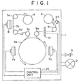
- Fig. 1 is a plan view showing a configuration example of an optical thin layer forming apparatus 1 as a preferred embodiment of the present invention.
- the optical thin layer forming apparatus or optical component producing apparatus 1 is used for forming optical thin layers on a base such as a high polymer film.
- Specific examples of the optical components produced by the apparatus 1 may include an dichroic mirror used for a projection television, an UV-IR filter (ultraviolet rays and infrared rays cutting filter), and a band filter. The following description will be made by using a dichroic mirror as an optical component.
- the optical thin layer forming apparatus 1 has a feed roll 4 (film formation means), a winding roll 6 (film formation means), guide rolls 5a, 5b, 5c, 5d, 5e, and 5f (film formation means), a plasma electrode 8 (film formation means), evaporation sources 7a and 7b (film formation means), and an optical monitor 10 (measurement means).
- a gas lead valve 9 and an evacuation system 2 are connected to the apparatus 1.
- the apparatus 1 has removal means 27.
- a running system for running, at a constant speed, a base 3a from the feed roll 4 to the winding roll 6 by way of the guide rolls 5a, 5b, 5c, 5d, and 5f.
- the plasma electrode 8, which is used for preparation such as degassing of the base 3a, is opposed to a portion, disposed between the guide rolls 5a and 5b, of the base 3a.
- the evaporation sources 7a and 7b, each of which is configured typically as a sputtering system, are disposed with their targets opposed to the guide roll 5d.
- the target is made from Si, Nb or the like as an optical thin layer material.
- the gas lead valve 9, which is connected to the apparatus 1, is used for adjusting, upon sputtering, the flow rate of a reaction gas to be supplied in the apparatus 1 such as argon (Ar) gas or oxygen gas.
- a reaction gas such as argon (Ar) gas or oxygen gas.
- the guide roll 5d has a cooled structure for preventing the temperature rise of the base 3a upon film formation.
- the optical monitor 10 is used for measuring an optical characteristic of an optical component obtained by forming optical thin layers on the surface of the base 3a.
- the optical characteristic to be measured is represented by a light transmittance, preferably, a mean light transmittance of an optical component. Since the apparatus 1 has the optical monitor 10, it can accurately measure a mean light transmittance of an optical component obtained by forming a multi-layer film having a plurality of optical thin layers.
- the apparatus 1 can remove the above excess layer portion, the layer thickness can be finely adjusted. Accordingly, the apparatus 1 can produce an optical component having a good optical characteristic.
- Fig. 2 is a block diagram showing a configuration example of the optical monitor 10 shown in Fig. 1.
- the optical monitor 10 includes an optical source 10c, an optical head 10g, and a spectroscope 10d.
- the optical monitor 10 preferably further includes a switch 10f. These devices are connected to each other via optical communication lines such as optical fibers except for a signal line for connecting the spectroscope 10d to the control unit 25.
- the optical head 10g has a light emitting unit 12 and a light receiving unit 13.
- the light emitting unit 12 is a light source enabling continuous emission of light having a wavelength of 450 to 700 nm, that is, a light source having a continuous spectrum of 450 to 700 nm in wavelength.
- the light emitting unit 12 is configured as an LED (Light Emitting Device).
- the light receiving unit 13 is configured as a photodiode for detecting a continuous spectrum of 450 to 700 nm in wavelength.
- the light emitting unit 12 and the light receiving unit 13 are opposed to each other with the running base 3a put therebetween.
- the light emitting unit 12 is connected to the light source 10c.
- the light source 10c is, in principle, supplies a specific quality of light.
- An optical communication line 10b extending from the switch 10f is connected to a mid point of the communication line between the light emitting unit 12 and the light source 10c.
- the light receiving unit 13 is connected to the spectroscope 10d, and preferably, the switch 10f to which the optical communication line 10b is connected is provided between the light receiving unit 13 and the spectroscope 10d.
- the light receiving unit 13 receives a light component, passing through the base 3a, of light emitted from the light emitting unit 12.
- the switch 10f detects a variation in quality of light emitted from the light source 10c by way of the optical communication line 10b. Accordingly, if the quality of light emitted from the light source 10c varies, the spectroscope 10d can detect a rate of the quality of light received by the light receiving unit 13 to the quality of light emitted from the light emitting unit 12 in consideration of the increased/decreased quality of light.
- the spectroscope 10d is connected to the control unit 25 and is controlled by the control unit 25.
- the spectroscope 10d can accurately calculate a rate (transmittance) of a light component, passing through the base 3a, of light emitted from the light emitting unit 12 by the function of the switch 10f. The transmittance thus calculated is supplied to the control unit 25.
- the control unit 25 controls a thickness of a portion of the multi-layer film to be formed on the optical component on the basis of the transmittance (or mean transmittance) thus supplied thereto.
- one film layer (tuning layer 32 in Fig. 3) having a higher refractive index and being positioned near the uppermost surface remotest from the base is controlled by the control unit 25.
- the tuning layer 32 which is a higher refractive index layer of the multi-layer film composed of layers different in refractive index to be described later, exerts a large effect on the optical characteristic of the optical component.
- the thickness of the tuning layer 32 by means of the control unit 25, it is possible to produce an optical component having a good optical characteristic.
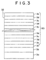
- Fig. 3 is a sectional view showing one example of a cross-sectional structure of an optical component formed by the optical thin layer forming apparatus 1 shown in Fig. 1.
- An optical component includes the base 3a, a hard coat layer 3b, a lower refractive index layer 3c', and a multi-layer film 30, which are arranged in this order from bottom to top.
- the multi-layer film 30 is obtained by forming lower refractive index layers 3c and higher refractive index layers 3d one by one in such a manner that the layers 3c and 3d are alternately stacked.
- the optical component is obtained by repeating alternative stacking of the lower refractive index layers 3a and higher refractive index layers 3d by 21 times on the base 3a covered with the hard coat layer 3b via the lower refractive index layer 3c'.
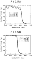
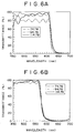
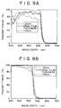
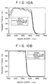
- Figs. 4A to 11B are characteristic diagrams showing examples of transmittance distributions relative to wavelengths of light.
- the abscissa indicates the wavelength (nm) and the ordinate indicates the transmittance (%).
- values described beside curves showing optical characteristics in each of Figs. 4A to 11B designate thicknesses of the tuning layers 32.
- Fig. 4A shows optical characteristics for light incident on the base 3a in the vertical direction, which are examples of optical characteristics showing the results outputted from the optical monitor 10
- Fig. 4B shows optical characteristics for light incident on the base 3a at an angle of 45° with respect to the vertical direction, which are examples of optical characteristics of optical components (dichroic mirrors in this embodiment).
- Figs. 4A to Fig. 7B show the transmittance characteristics relative to wavelengths of light for an optical component including the multi-layer film 30 obtained by stacking the lower refractive index layers 3c, higher refractive index layers 3d, lower refractive index layers 3c, . . . , higher refractive index layers 3d, and lower refractive index layers 3c in this order from bottom to top.
- the tuning layer 32 is set at the 18th layer in Figs. 4A and 4B, the 19th layer in Figs. 5A and 5B, the 20th layer in Figs. 6A and 6B, and the 21st layer in Figs. 7A and 7B.
- the optical characteristic of the higher refractive index layer 3d is changed larger than the optical characteristic of the lower refractive index layer 3c does.
- the transmittance in the case where the tuning layer 32 is taken as the 20th higher refractive index layer 3d, the transmittance becomes the peak value at the ideal thickness in the transmission wavelength band (450 to 550 nm); while in the case where the tuning layer 32 is taken as the 18th high refractive index layer 3d, the transmittance does not become the peak value at the ideal thickness in the transmission wavelength band (450 to 550 nm).
- Figs. 8A to Fig. 11B show the transmittance characteristics relative to wavelengths of light for an optical component including the multi-layer film 30 obtained by stacking the higher refractive index layers 3d, lower refractive index layers 3c, higher refractive index layers 3d, . . ., lower refractive index layers 3c and higher refractive index layers 3d in this order from bottom to top.
- the tuning layer 32 is set at the 18th layer in Figs. 8A and 8B, the 19th layer in Figs. 9A and 9B, the 20th layer in Figs. 10A and 10B, and the 21st layer in Figs. 11A and 11B.
- the optical characteristic of the higher refractive index layer 3d is changed larger than that of the lower refractive index layer 3c.
- the transmittance becomes the peak value at the ideal thickness in the transmission wavelength band (450 to 550 nm); while in the case where the tuning layer 32 is taken as the 19th high refractive index layer 3d, the transmittance does not become the peak value at the ideal thickness in the transmission wavelength band (450 to 550 nm).
- the higher refractive index film 3d positioned near the uppermost surface remotest from the base 3a be set as the tuning layer 32.
- the base 3a having a thickness of 188 ⁇ m, made from polyethylene naphthalate, is set on the feed roll 4 to be wound around the winding roll 6 by way of the guide rolls 5a, 5b, 5c, 5d, 5e, and 5f.
- An SiOx (x is a positive number of 2 or less) is formed on the base 3a by sputtering the evaporation source 7a having an Si target while adjusting a flow rate of each of Ar gas and oxygen gas. Subsequently, 21 optical thin layers made from SiO 2 and Nb 2 O 5 are formed one by one to satisfy a predetermined optically designed configuration by alternately sputtering the evaporation source 7b having an Nb target and the evaporation source 7a having the Si target while adjusting a flow rate of each of Ar gas and oxygen gas. In addition, the SiOx layer is taken as one of the SiO 2 layers of the above 21 layers.
- the flow rate of each of Ar gas and oxygen gas for sputtering is adjusted by the gas lead valve 9 to change the sputtering pressure.
- the sputtering pressure used in this embodiment is set at about 1.6 Pa, to reduce the entire internal stress of the optical thin layers while adjusting the balance in stress between SiO 2 and Nb 2 O 5 , thereby reducing a curling of the film-like base 3a.
- a hard coat layer is formed on the surface on which optical thin layers are to be formed, and an adhesive layer is formed on the opposed surface to the optical thin layer formation surface and a protective film is formed on the adhesive layer.
- the base 3a made from polyethylene naphthalate has a high heat resistance, that is, a high resistance against thermal deformation, optical thin layers can be uniformly formed on the base 3a.
- polyethylene naphthalate having a glass transition point of 110°C is superior in heat resistance to polyethylene terephthalate having a glass transition point of 69°C.
- a glass plate having a width of 5 cm, a length of 8.75 cm, and a thickness of 1 mm is prepared as a transparent member.
- the base 3a, on which the optical thin layers have been formed, is laminated on the transparent member via an adhesive, and is then cut into a size matched to that of the glass plate. In this way, an optical component applicable to a dichroic mirror used for typically a projection television is finished.
- a protective film formed on an adhesive layer may be used as the transparent member.
- the optical monitor 10 is essential for stably producing an optical component (optical filter) having a high quality.
- Fig. 12 is a diagram showing one example of simulation of a change in mean transmittance in the case of gradually increasing the thickness of an optical thin layer by using the optical monitor
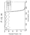
- Fig. 13 is a diagram showing one example of a difference in final transmittance distribution between an optical component in which the thickness adjustment by using the optical monitor is performed and an optical component in which the thickness adjustment by using the optical monitor is performed.
- Fig. 12 shows a change in mean transmittance in the case of changing the thickness of the tuning layer 32 by about ⁇ 20 ⁇ m in the case where light is made incident on the base in the vertical direction.
- the ideal thickness of the tuning layer is typically 94.76 nm.
- the mean transmittance of the tuning layer 32 is increased as the thickness thereof is gradually increased from 74.76 nm, reaching the peak value when the thickness of the layer 32 is increased to about 94.76 nm, and is changed to be decreased as the thickness of the layer 32 is further increased. Further, as shown in Fig.
- the mean transmittance in a transmission wavelength band (450 to 550 nm) of the optical component in which the thickness adjustment by using the optical monitor 10 is performed is about 7% higher than that of the optical component in which the thickness adjustment by using the optical monitor 10 is not performed. Accordingly, it is possible to produce an optical component having a high quality by using the optical monitor 10.
Landscapes
- Chemical & Material Sciences (AREA)
- Organic Chemistry (AREA)
- Engineering & Computer Science (AREA)
- Materials Engineering (AREA)
- Mechanical Engineering (AREA)
- Metallurgy (AREA)
- Chemical Kinetics & Catalysis (AREA)
- Physics & Mathematics (AREA)
- General Physics & Mathematics (AREA)
- Optics & Photonics (AREA)
- Optical Filters (AREA)
- Surface Treatment Of Optical Elements (AREA)
- Laminated Bodies (AREA)
- Physical Vapour Deposition (AREA)
- Chemical Vapour Deposition (AREA)
Abstract
Description
Claims (8)
- An optical component producing apparatus for forming a multi-layer film, which is composed of alternately stacked layers different in optical characteristic, on a base, said apparatus comprising:film formation means for forming said multi-layer film on said base;measurement means for measuring an optical characteristic of said optical component obtained by forming said multi-layer film on said base; andcontrol means for controlling a thickness of a portion of said multi-layer film to be formed by said film formation means on the basis of the measured optical characteristic of said optical component.
- An optical component producing apparatus according to claim 1, wherein said measurement means measures a transmittance of said optical component; andsaid control means terminates the film formation by said film formation means at said portion of said multi-layer film when said measured transmittance of said optical component is changed to be decreased.
- An optical component producing apparatus according to claim 2, further comprising removal means for removing the layer portion formed during a period of time from a time point when the increase/decrease of the measured transmittance of said optical component is stopped to a time point when the measured transmittance is changed to be decreased.
- An optical component producing apparatus according to claim 1, wherein said control means controls a thickness of one layer of said plurality of alternately stacked layers, said one layer having a higher refractive index and being positioned near the uppermost surface remotest from said base.
- An optical component producing method for forming a multi-layer film, which is composed of alternately stacked layers different in optical characteristic, on a base, said method comprising:measuring an optical characteristic of said optical component obtained by forming said multi-layer film on said base; andcontrolling, on the basis of the measured optical characteristic of said optical component, a thickness of a portion of said multi-layer film to be formed on said base.
- An optical component producing method according to claim 5, wherein said measurement step comprises the step of measuring a transmittance of said optical component; andsaid control step comprises the step of terminating the film formation at said portion of said multi-layer film when said measured transmittance of said optical component is changed to be decreased.
- An optical component producing method according to claim 6, further comprising removal step of removing a layer portion formed during a period of time from a time point when the increase/decrease of the measured mean light transmittance of said optical component is stopped to a time point when the measured mean light transmittance is changed to be decreased.
- An optical component producing method according to claim 5, wherein said control steps comprises the step of controlling a thickness of one layer of said plurality of alternately stacked layers, said one layer having a higher refractive index and being positioned near the uppermost surface remotest from said base.
Applications Claiming Priority (2)
| Application Number | Priority Date | Filing Date | Title |
|---|---|---|---|
| JP29440699 | 1999-10-15 | ||
| JP29440699A JP4345158B2 (en) | 1999-10-15 | 1999-10-15 | Optical component manufacturing apparatus and manufacturing method |
Publications (2)
| Publication Number | Publication Date |
|---|---|
| EP1094341A2 true EP1094341A2 (en) | 2001-04-25 |
| EP1094341A3 EP1094341A3 (en) | 2002-08-28 |
Family
ID=17807342
Family Applications (1)
| Application Number | Title | Priority Date | Filing Date |
|---|---|---|---|
| EP00122454A Withdrawn EP1094341A3 (en) | 1999-10-15 | 2000-10-13 | Apparatus and method for producing optical component |
Country Status (3)
| Country | Link |
|---|---|
| US (1) | US6733821B1 (en) |
| EP (1) | EP1094341A3 (en) |
| JP (1) | JP4345158B2 (en) |
Cited By (1)
| Publication number | Priority date | Publication date | Assignee | Title |
|---|---|---|---|---|
| JP2001116902A (en) * | 1999-10-15 | 2001-04-27 | Sony Corp | Optical component manufacturing apparatus and manufacturing method |
Families Citing this family (2)
| Publication number | Priority date | Publication date | Assignee | Title |
|---|---|---|---|---|
| EP2826883B1 (en) * | 2013-07-17 | 2018-10-03 | Applied Materials, Inc. | Inline deposition control apparatus and method of inline deposition control |
| JP6852987B2 (en) * | 2016-06-07 | 2021-03-31 | 日東電工株式会社 | Multilayer film formation method |
Family Cites Families (17)
| Publication number | Priority date | Publication date | Assignee | Title |
|---|---|---|---|---|
| GB2029017B (en) * | 1978-08-18 | 1982-10-13 | Holland L | Control of deposition of thin films |
| CH634424A5 (en) * | 1978-08-18 | 1983-01-31 | Nat Res Dev | METHOD AND APPARATUS FOR DETECTING AND CONTROLLING THE DEPOSITION OF A FINE FILM. |
| JPS5530172A (en) * | 1978-08-25 | 1980-03-03 | Mitsubishi Electric Corp | Forming conductive layers on glass |
| GB8612358D0 (en) * | 1986-05-21 | 1986-06-25 | Philips Nv | Cathode ray tube |
| US5483378A (en) * | 1988-04-19 | 1996-01-09 | Litton Systems, Inc. | Fault tolerant anti-reflective coatings |
| JPH03226573A (en) * | 1990-01-31 | 1991-10-07 | Shin Meiwa Ind Co Ltd | Thin film thickness control method |
| JPH0772307A (en) * | 1993-09-03 | 1995-03-17 | Canon Inc | Thin film forming method and apparatus |
| JPH0770749A (en) * | 1993-09-03 | 1995-03-14 | Canon Inc | Thin film forming method and apparatus |
| US5911856A (en) * | 1993-09-03 | 1999-06-15 | Canon Kabushiki Kaisha | Method for forming thin film |
| JPH0790593A (en) * | 1993-09-17 | 1995-04-04 | Hitachi Ltd | Film forming apparatus and film forming method |
| KR950034499A (en) * | 1994-01-28 | 1995-12-28 | 제임스 조셉 드롱 | Method and apparatus for monitoring the deposition rate of films during physical vapor deposition |
| JPH0882701A (en) * | 1994-09-13 | 1996-03-26 | Sumitomo Chem Co Ltd | Anti-reflection film manufacturing method |
| US5541470A (en) * | 1994-12-02 | 1996-07-30 | Osram Sylvania Inc. | Method for making a tantala/silica interference filter on a vitreous substrate and an electric lamp made thereby |
| TW320687B (en) * | 1996-04-01 | 1997-11-21 | Toray Industries | |
| US6217720B1 (en) * | 1997-06-03 | 2001-04-17 | National Research Council Of Canada | Multi-layer reactive sputtering method with reduced stabilization time |
| JPH11119002A (en) * | 1997-10-17 | 1999-04-30 | Sony Corp | Optical component manufacturing apparatus, optical component manufacturing method using the same, optical component, and projection television using the optical component |
| JP4345158B2 (en) * | 1999-10-15 | 2009-10-14 | ソニー株式会社 | Optical component manufacturing apparatus and manufacturing method |
-
1999
- 1999-10-15 JP JP29440699A patent/JP4345158B2/en not_active Expired - Lifetime
-
2000
- 2000-10-13 EP EP00122454A patent/EP1094341A3/en not_active Withdrawn
- 2000-10-16 US US09/688,541 patent/US6733821B1/en not_active Expired - Fee Related
Cited By (1)
| Publication number | Priority date | Publication date | Assignee | Title |
|---|---|---|---|---|
| JP2001116902A (en) * | 1999-10-15 | 2001-04-27 | Sony Corp | Optical component manufacturing apparatus and manufacturing method |
Also Published As
| Publication number | Publication date |
|---|---|
| JP4345158B2 (en) | 2009-10-14 |
| US6733821B1 (en) | 2004-05-11 |
| JP2001116902A (en) | 2001-04-27 |
| EP1094341A3 (en) | 2002-08-28 |
Similar Documents
| Publication | Publication Date | Title |
|---|---|---|
| CN101441279B (en) | Ultra low residual reflection low stress lens coating | |
| KR100972769B1 (en) | An optical film thickness control method, an optical film thickness control device, a dielectric multilayer film production device, and a dielectric multilayer film made with such a control device or production device | |
| JP3290629B2 (en) | Optical multilayer filter | |
| US20060087602A1 (en) | Polarizer and method for producing it | |
| US4931315A (en) | Wide angle optical filters | |
| US6111698A (en) | Multilayer absorbing antireflective coating | |
| US7440204B2 (en) | ND filter of optical film laminate type with carbon film coating | |
| JPH11249067A (en) | Observation system having half mirror and method of manufacturing the half mirror | |
| US20030081319A1 (en) | Tunable optical filter | |
| US6733821B1 (en) | Method for forming an optical component | |
| JP4623349B2 (en) | Thin film type ND filter and manufacturing method thereof | |
| US20060285208A1 (en) | Optical multilayer thin-film system | |
| JPH11119002A (en) | Optical component manufacturing apparatus, optical component manufacturing method using the same, optical component, and projection television using the optical component | |
| CN1417617A (en) | Intelligent film filter | |
| JP2003107242A (en) | UV cut filter | |
| US5812264A (en) | Method of measuring surface reflectance and a method of producing antireflective polarizing film | |
| JP4963027B2 (en) | ND filter, method for manufacturing the same, and light quantity reduction device using them | |
| JP2004061810A (en) | Apparatus for forming multilayer optical filter and method for manufacturing multilayer optical filter | |
| JP2003302521A (en) | Optical multilayer filter | |
| JP2005107010A (en) | Method for manufacturing multilayer optical filter, and multilayer optical filter | |
| JP2874439B2 (en) | Optical wavelength tunable filter and method of manufacturing the same | |
| US20090002816A1 (en) | Selective Reflecting for Laser Projector | |
| JP3754874B2 (en) | Film forming method and film forming apparatus | |
| JP2000171607A (en) | Highly dense multilayer thin film and method for forming the same | |
| US20030103726A1 (en) | Optical device |
Legal Events
| Date | Code | Title | Description |
|---|---|---|---|
| PUAI | Public reference made under article 153(3) epc to a published international application that has entered the european phase |
Free format text: ORIGINAL CODE: 0009012 |
|
| AK | Designated contracting states |
Kind code of ref document: A2 Designated state(s): AT BE CH CY DE DK ES FI FR GB GR IE IT LI LU MC NL PT SE |
|
| AX | Request for extension of the european patent |
Free format text: AL;LT;LV;MK;RO;SI |
|
| PUAL | Search report despatched |
Free format text: ORIGINAL CODE: 0009013 |
|
| AK | Designated contracting states |
Kind code of ref document: A3 Designated state(s): AT BE CH CY DE DK ES FI FR GB GR IE IT LI LU MC NL PT SE |
|
| AX | Request for extension of the european patent |
Free format text: AL;LT;LV;MK;RO;SI |
|
| RIC1 | Information provided on ipc code assigned before grant |
Free format text: 7G 02B 5/00 A, 7C 23C 14/54 B, 7C 23C 16/52 B, 7G 01B 21/08 B |
|
| 17P | Request for examination filed |
Effective date: 20030129 |
|
| 17Q | First examination report despatched |
Effective date: 20030324 |
|
| AKX | Designation fees paid |
Designated state(s): DE FR GB NL |
|
| STAA | Information on the status of an ep patent application or granted ep patent |
Free format text: STATUS: THE APPLICATION IS DEEMED TO BE WITHDRAWN |
|
| 18D | Application deemed to be withdrawn |
Effective date: 20040127 |