EP1093181A2 - Nonreciprocal circuit device and communication device using same - Google Patents
Nonreciprocal circuit device and communication device using same Download PDFInfo
- Publication number
- EP1093181A2 EP1093181A2 EP00122447A EP00122447A EP1093181A2 EP 1093181 A2 EP1093181 A2 EP 1093181A2 EP 00122447 A EP00122447 A EP 00122447A EP 00122447 A EP00122447 A EP 00122447A EP 1093181 A2 EP1093181 A2 EP 1093181A2
- Authority
- EP
- European Patent Office
- Prior art keywords
- circuit device
- nonreciprocal circuit
- magnet
- center
- electrodes
- Prior art date
- Legal status (The legal status is an assumption and is not a legal conclusion. Google has not performed a legal analysis and makes no representation as to the accuracy of the status listed.)
- Withdrawn
Links
- 238000004891 communication Methods 0.000 title claims description 10
- 239000000758 substrate Substances 0.000 claims abstract description 20
- 239000004020 conductor Substances 0.000 claims abstract description 13
- 239000003990 capacitor Substances 0.000 claims description 23
- 238000009413 insulation Methods 0.000 claims description 23
- 230000005291 magnetic effect Effects 0.000 claims description 17
- 230000005293 ferrimagnetic effect Effects 0.000 claims description 15
- 125000006850 spacer group Chemical group 0.000 claims description 11
- 230000003068 static effect Effects 0.000 claims description 10
- 239000011888 foil Substances 0.000 claims description 2
- 239000012212 insulator Substances 0.000 claims description 2
- 239000002184 metal Substances 0.000 claims description 2
- 229910052751 metal Inorganic materials 0.000 claims description 2
- 238000003780 insertion Methods 0.000 abstract description 31
- 230000037431 insertion Effects 0.000 abstract description 31
- 229910000859 α-Fe Inorganic materials 0.000 abstract description 22
- 229910000679 solder Inorganic materials 0.000 abstract description 19
- 239000011347 resin Substances 0.000 abstract description 7
- 229920005989 resin Polymers 0.000 abstract description 7
- 238000002955 isolation Methods 0.000 description 12
- 230000005540 biological transmission Effects 0.000 description 9
- 238000010586 diagram Methods 0.000 description 8
- 239000003302 ferromagnetic material Substances 0.000 description 5
- 230000010355 oscillation Effects 0.000 description 4
- 239000002902 ferrimagnetic material Substances 0.000 description 3
- RYGMFSIKBFXOCR-UHFFFAOYSA-N Copper Chemical group [Cu] RYGMFSIKBFXOCR-UHFFFAOYSA-N 0.000 description 2
- 239000011889 copper foil Substances 0.000 description 2
- 230000008878 coupling Effects 0.000 description 2
- 238000010168 coupling process Methods 0.000 description 2
- 238000005859 coupling reaction Methods 0.000 description 2
- 230000003247 decreasing effect Effects 0.000 description 2
- 238000011835 investigation Methods 0.000 description 2
- 238000000465 moulding Methods 0.000 description 2
- 230000010287 polarization Effects 0.000 description 2
- 229920006395 saturated elastomer Polymers 0.000 description 2
- 230000000052 comparative effect Effects 0.000 description 1
- 238000002474 experimental method Methods 0.000 description 1
- 238000004519 manufacturing process Methods 0.000 description 1
- 238000000034 method Methods 0.000 description 1
- 238000000059 patterning Methods 0.000 description 1
- 230000008054 signal transmission Effects 0.000 description 1
Images






Classifications
-
- H—ELECTRICITY
- H01—ELECTRIC ELEMENTS
- H01P—WAVEGUIDES; RESONATORS, LINES, OR OTHER DEVICES OF THE WAVEGUIDE TYPE
- H01P1/00—Auxiliary devices
- H01P1/32—Non-reciprocal transmission devices
- H01P1/38—Circulators
- H01P1/383—Junction circulators, e.g. Y-circulators
- H01P1/387—Strip line circulators
-
- H—ELECTRICITY
- H01—ELECTRIC ELEMENTS
- H01P—WAVEGUIDES; RESONATORS, LINES, OR OTHER DEVICES OF THE WAVEGUIDE TYPE
- H01P1/00—Auxiliary devices
- H01P1/32—Non-reciprocal transmission devices
-
- H—ELECTRICITY
- H01—ELECTRIC ELEMENTS
- H01P—WAVEGUIDES; RESONATORS, LINES, OR OTHER DEVICES OF THE WAVEGUIDE TYPE
- H01P1/00—Auxiliary devices
- H01P1/32—Non-reciprocal transmission devices
- H01P1/36—Isolators
-
- H—ELECTRICITY
- H01—ELECTRIC ELEMENTS
- H01P—WAVEGUIDES; RESONATORS, LINES, OR OTHER DEVICES OF THE WAVEGUIDE TYPE
- H01P1/00—Auxiliary devices
- H01P1/32—Non-reciprocal transmission devices
- H01P1/38—Circulators
- H01P1/383—Junction circulators, e.g. Y-circulators
Definitions
- the present invention relates to a nonreciprocal circuit device such as an isolator, a gyrator, or the like to operate in a microwave band or the like, and a communication device including the same.
- Nonreciprocal circuit devices to operate in a microwave band or the like are disclosed in U.S. Patent No.4016510, Japanese Unexamined Patent Application Publication No. 52-134349, Japanese Unexamined Patent Application Publication No. 58-3402, Japanese Unexamined Patent Application Publication No. 9-232818, and Japanese Unexamined Patent Application Publication No. 8-8612.
- center electrodes intersecting each other at a predetermined angle are provided on a ferrite sheet, and a static magnetic field is applied to the ferrite sheet.
- a nonreciprocal characteristic is presented by rotating the polarization plane of a high frequency magnetic field generated by the center electrodes, based on the Faraday's rotation principle, utilizing the ferrimagnetic characteristic of the ferrite sheet.
- the matching impedance of the third center electrode has a reactance component, and the impedance depends on the frequency. Accordingly, the frequency range where a good nonreciprocal characteristic can be obtained is narrow. That is, when the nonreciprocal circuit device is used as an isolator, the isolation characteristic inevitably becomes narrow.
- the inventors of the present invention has made intensive investigation and experiment in order to provide a nonreciprocal circuit device having a good nonreciprocal characteristic in a wide band.
- the inventors have found the cause by which the insertion loss is deteriorated in a wide band.
- a high frequency current flows through a permanent magnet (hereinafter, referred to as a magnet briefly), and power is consumed, due to the electric resistance of the magnet. This is cause for increase of the insertion loss.
- a nonreciprocal circuit device which comprises a first center electrode of which one of the ends is connected to an input terminal, and the other end is grounded, a second center electrode intersecting the first center electrode in insulation state between the electrodes, one end of the second center electrode being connected to an output terminal, the other end thereof being grounded, a ferrimagnetic member provided in adjacent to the first and second center electrodes, a magnet for applying a static magnetic field to the ferrimagnetic member substantially perpendicular to the ferrimagnetic member, a first capacitor of which one of the ends is connected to the input terminal and the other end is grounded, a second capacitor of which one of the ends is connected to the output terminal, and the other end is grounded, and an insulation spacer provided between the magnet and the first or second center electrode, whereby power consumption, caused when a high frequency magnetic field, generated by the center electrodes, passes through the magnet so that a high frequency current flows in the magnet, can be suppressed.
- the center electrodes are prevented from contacting closely with the magnet, and coupling between the high frequency magnetic field generated in the first and second electrodes and the magnet is weakened.
- the conductor loss attributed to the high frequency current induced in the magnet, can be reduced.
- the first and second center electrodes comprise conductor patterns formed on the opposite sides of a substrate, respectively, and resist films are formed on the surfaces of the conductor patterns.
- the resist films are used as the insulation spacers.
- a resistor to be connected between the input terminal and the output terminal may be mounted onto the substrate having the center electrodes.
- the conductor patterns each comprise a metal foil having a thickness of at least 30 ⁇ m, and the resist films have a thickness of at least 50 ⁇ m.
- an insulation film may be bonded to the magnet.
- the insulation film is used as the insulation spacer between the magnet and the center electrodes.
- intersection angle between the first and second center electrodes may be a predetermined angle between 90° and 100° inclusive. Thereby, a desired isolation characteristic can be obtained.
- the ferrimagnetic member has a substantially rectangular parallelepiped shape.
- the center electrodes are arranged in the diagonal directions of the ferrimagnetic member.
- the long center electrodes can be efficiently arranged. That is, the nonreciprocal circuit device of the present invention, even though the ferrimagnetic member is small in size, has a low loss characteristic.
- the capacitances of the first and second capacitors are substantially the same. Therefore, even if the inductances of the first and second electrodes has a difference, a desired isolation characteristic can be obtained by setting the difference between the phase of a transmission signal in the forward direction from the input terminal to the output terminal and the phase of a transmission signal in the reverse direction from the output terminal to the input terminal at approximately 180°.
- the first and second center electrodes, the ferrimagnetic member, the magnet, and the first and second capacitors are surrounded by yokes to be shielded, respectively, the yokes constituting a magnetic circuit for applying the static magnetic field, and the yokes have a ground potential.
- the first and second center electrodes and the capacitors have a ground potential together with the yokes to be shielded.
- an insulator layer is provided between the yoke and the center electrode.
- the yoke is separated from the center electrode, so that high frequency current generated in the yoke is suppressed, the Q value is enhanced, and the insertion loss is reduced.
- plural earth terminals are provided, at least two of the earth terminals and the input terminal are provided in one of the sides of the case, and at least two of the remaining earth terminals and the output terminal are provided in the other side of the case.
- the ground connection is enhanced, so that unnecessary inductance or static capacitance components are suppressed, directly-reached waves from the input terminal to the output terminal are decreased, and the band width (the bandwidth indicating a low insertion loss characteristic) is widened.
- a communication device which includes the above-described nonreciprocal circuit device.
- the nonreciprocal circuit device is provided in the output section of an oscillation circuit, the input section of a filter, or the like to form the communication device.
- Fig. 1 is an exploded perspective view of the isolator.
- a resin case 1 is formed by insert molding, using input-output terminals 2a and 2b and an earth terminal 3, One 2a of the input-output terminals is shown.
- the other input-output terminal 2b and the other two earth terminals 3 are formed on the left-back side face in Fig. 1 of the resin case 1.
- the inner ends of the two input-output terminals 2a and 2b are exposed on the inner bottom surface of the resin case 1.
- the isolator includes a ferrite sheet 5 made of a ferrimagnetic material, capacitors 7a and 7b having capacitor electrodes provided on the upper and lower surfaces thereof, a chip resistor 8, and a lower yoke 9 made of a ferromagnetic material 9.
- the capacitors 7a and 7b, and the chip resistor 8 are disposed in the case 1.
- the ferrite sheet 5 is placed in the concavity defined by the case 1 and the lower yoke 9.
- a first center electrode 4a and a second center electrode 4b are formed so as to intersect with each other at a predetermined intersection angle between 90° and 100° on the upper and under faces of an insulation sheet 14.
- One ends of the two center electrodes 4a and 4b are led out via through-holes to the under side in Fig. 1.
- the other ends of the center electrodes 4a and 4b are connected to each other via through-holes.
- the substrate 14 is formed by patterning a high frequency circuit substrate, which is an insulation substrate having copper foils bonded to both of the sides thereof.
- a magnet 6 is disposed to apply a static magnetic field to the center electrodes 4a and 4b and the ferrite sheet 5.
- An upper yoke 10 is formed from a ferromagnetic material.
- An upper yoke 10 is made of a ferromagnetic material. The magnet 6 is attached to the inner face (the lower face in Fig. 1) of the upper yoke 10.
- the respective parts of the isolator are formed as described above.
- the ferrite sheet 5 is accommodated in the case 1.
- the capacitors 7a and 7b are placed therein, and the substrate 14 is disposed in such a manner that the capacitors 7a and 7b are sandwiched between the substrate 14 and the case 1.
- the chip resistor 8 is mounted to the under face of the substrate 14 in such a manner as to connect the ends of the first and second center electrodes 4a and 4b to each other.
- the lower yoke 9 is attached to the underside of the case 1.
- the upper yoke 10 having the magnet 6 attached thereto is made to cover the case 1.
- an isolator as a whole is formed.
- Fig. 2 is a cross section of an major part of the above-described isolator.
- solder resist films 11 are formed on both of the whole faces of substrate 14, respectively.
- the resist films 11 lie over the surfaces of the first and second center electrodes 14, respectively.
- the magnet 6 is disposed closely to the substrate 14, the magnet 6 and the first center electrode 4a are separated from each other by the thickness of the solder resist film 11.
- the center electrode and the upper yoke are further separated from each other by the layer of the solder resist film.
- the ferrite sheet 5 and the second center electrode 4b are separated from each other at least by the thickness of the solder resist film 11.
- the thickness of the above-mentioned solder resist film 11 is at least 50 ⁇ m, and that of the respective first and second center electrodes is at least 30 ⁇ m.
- Fig. 12A shows the relation of the distance between the magnet 6 and the center electrode 4a, to the insertion loss (IL).
- a high frequency current flows in the magnet 6, caused by an eddy current, so that power is consumed, due to the electric resistance of the magnet 6.
- the magnet 6 has a large dielectric loss tangent ( tan ⁇ ).
- the dielectric loss is increased.
- the center electrodes and the magnet, and also, the center electrodes and the yokes are separated from each other by means of the solder resist films, respectively.
- the insertion loss (IL) is changed with the thickness of the solder resist film, as shown in Fig. 12A.
- the insertion loss is 1.3 dB.
- the insertion loss required for isolators having the above outer size is up to 1.3 dB. Therefore, the thickness of each of the above-described solder resist films is set at 50 ⁇ m or more.
- Fig. 12B shows a relation between the thickness of each center electrode and the insertion loss (IL).
- the thickness of the solder resist film is set at 50 ⁇ m, as seen in the above description.
- the insertion loss (IL) changes with the thickness of the center electrode being varied, as shown in Fig. 12B.
- the larger the thickness of the center electrode is the smaller the insertion loss (IL) becomes, and is rapidly saturated when the thickness exceeds about 30 ⁇ m.
- the insertion loss is 1.3 dB.
- the required insertion loss is generally up to 1.3 dB. Accordingly, the thickness of each of the center electrodes 4a and 4b is set at 30 ⁇ m or larger. For the purpose of reducing the height of the isolator as much as possible, the thickness of each of the center electrodes 4a and 4b is set at approximately 40 ⁇ m.
- Fig. 3 is a circuit diagram of the above-described isolator.
- the ferrite sheet 5 has a disk-shape.
- the first center electrode 4a is connected between the input terminal 2a and the earth terminal 3
- the second center electrode 4b is connected between the output terminal 2b and the earth terminal 3
- a capacitor C1 is connected between the input terminal 2a and the earth terminal 3
- a second capacitor C2 is connected between the output terminal 2b and the earth terminal 3
- a resistor R is connected between the input terminal 2a and the output terminal 2b.
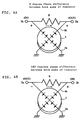
- Figs. 4A and 4B are circuit diagrams illustrating the operational principle of the above-described isolator.
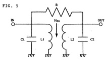
- Fig. 5 is an equivalent circuit diagram of the isolator.
- Figs. 4A and 4B the arrows indicate the directions of high frequency magnetic fields under the center electrodes. Now, the transmission of a signal in the forward direction will be described. At both of the ends of the resistor R, the same phases and the same amplitudes are produced, so that no current flows through the resistor R. An input signal from the input terminal 2a as it is output from the output terminal 2b.
- the intensity of an outer magnetic field and the intersection angle between the center electrodes 4a and 4b are determined in such a manner that a small insertion loss and a high isolation characteristic can be obtained.
- the intensity of a magnetic field applied to the ferrite sheet is 0.09 to 0.17 (T). Therefore, by setting the intersection angle between the center electrodes 4a and 4b to be in the range of 90° to 100°, a small insertion loss and a high isolation characteristic can be obtained.
- the phase difference between a signal S12 (propagation signal in the reverse direction) and a signal S21 (a transmission signal in the forward direction) becomes 180°, by removing the resistor R from the equivalent circuit diagram of Fig. 5. If the inductances L1 and L2 of the center electrodes 4a and 4b have a difference, the phase difference departs from 180°. However, by providing capacitors C1 and C2, and setting the static capacitances to be equal to each other, the above-mentioned departure of the phase difference can be prevented.
- the capacitances of the capacitors 7a and 7b are set to be substantially equal to each other with the difference of ⁇ 0.05 (5%) in order to set an isolation of at least 30 dB.
- Fig. 6 is a graph showing the insertion loss characteristic A of the isolator of this embodiment in comparison with that B of a conventional isolator, in which no solder resist film is provided on the surface of a substrate. As described above, by separating the center electrode from the magnet by means of the solder resist film formed on the surface of the substrate, the insertion loss can be reduced in a wide frequency range.
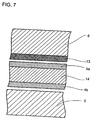
- Fig. 7 is a cross section of a major part of the isolator of the second embodiment. The cross section is shown correspondingly to that of the first embodiment of Fig. 2.
- an insulation film 13 is bonded to the surface on the substrate side of the magnet 6.
- no solder resist films are formed on the surfaces of the center electrodes 4a and 4b provided on both of the sides of the substrate 14, respectively.
- solder resist films may be formed on the surfaces of the substrate 14 having the center electrodes 4a and 4b formed thereon. Thereby, the magnet 6 and the center electrode 4a can be separated from each other by a predetermined distance by utilizing the thickness of the solder resist film and that of insulation film 13.
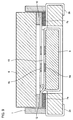
- Fig. 8 is an exploded perspective view of the isolator.
- a resin case 1 is formed by insert molding together with input-output terminals and earth terminals 3. One 2b of the input-output terminals is shown. The other input-output terminal and the other two earth terminals are provided on left-rear side in Fig. 8 of the resin case 1. The inner ends of the two input-output terminals are exposed on the inner bottom surface of the case 1.
- capacitors 7a and 7b having capacitor electrodes provided on the upper and lower surfaces thereof, and a chip resistor 8 are disposed, and a ferrite sheet 5 formed from a ferrimagnetic material is accommodated in the concavity defined by the case 1 and a lower yoke.
- Center electrodes 4a and 4b formed from copper foils, respectively, are provided so as to elongate from the upper face to the under face of the ferrite sheet 5 and intersect each other at a predetermined intersection angle in the diagonal directions of the ferrite sheet 5.
- a magnet 6 is provided to apply a static magnetic field to the center electrodes 4a and 4b and the ferrite sheet 5.
- An upper yoke 10 is formed from a ferromagnetic material. The magnet 6 is bonded to the inner face (the under face in Fig. 8) of the yoke 10.
- An insulation spacer 12 made of a resin sheet having a predetermined thickness separates the magnet 6 from the center electrodes 4a and 4b.
- a lower yoke 9 is formed from a ferromagnetic material.
- the respective parts of the isolator are formed as described above.
- the capacitors 7a and 7b and the chip resistor 8 are mounted in the case 1.
- the center electrodes 4a and 4b together with the ferrite sheet 5 are mounted therein.
- the capacitors 7a and 7b are sandwiched between the electrodes in the case 1 and the center electrodes 4a and 4b.
- the lower yoke 9 is attached to the underside of the case 1.
- the upper yoke 10 having the magnet 6 previously attached thereto is made to cover, whereby the isolator as a whole is formed.
- Fig. 9 is a cross section of a major part of the above-described isolator. In this figure, the lower and upper yokes 9 and 10 are omitted. As shown in Fig. 9, the center electrode 4a and the center electrode 4b are insulated from each other by means of the insulation film 15. The insulation spacer 12 is disposed so as to be interposed between the ends of the center electrodes 4a and 4b and the magnet 6, so that the magnet 6 and the center electrode 4b are kept at a predetermined interval.
- the each input-output impedance of the isolators is changed, depending on the thickness of the ferrite sheet and the length of the center electrodes.
- This embodiment uses the ferrite sheet 5 having such a thickness that the bottom surface of the ferrite sheet 5 is positioned above that of the case 1.
- the thickness of the case 1 may be reduced, so that the ground electrode portion of the center electrodes, provided on the under surface of the ferrite sheet, is brought into close contact with the lower yoke.
- Figs. 10A, 10B, 10C, and 10D are graphs showing the frequency characteristics of the above-described isolator.
- Figs. 11A, 11B. 11C, and 11D are graphs showing the frequency characteristics of an isolator as a contrast.
- Figs. 10A and 11A show the input reflection characteristics (S11)
- Figs. 10B and 11B show the transmission characteristics (S21)
- Figs. 10C and 11C show the isolation characteristics (S12)
- Figs. 10D and 11D show the output reflection characteristics (S22).
- the intersection angle of the two center electrodes is 90°, and the resistor is connected between the input-output terminals as shown in Fig. 5.
- the isolator having the characteristics graphed in Figs. 11A, 11B, 11C, and 11D includes three center electrodes with an intersection angle of 120°, and one end of the third center electrode is grounded via a resistor.
- the sized of the ferrite sheets employed in the two isolators are the same.
- the intersection angle is smaller than 120°, as described above, a good isolation characteristic can be obtained in a wide band.
- the insertion loss is reduced. Thereby, a small insertion loss in a wide frequency range and a good isolation characteristic in a wide band can be obtained.
- One of the above-described different types of isolators is provided in the oscillation output section of an oscillator such as VCO or the like, as shown in Fig. 13A, so that a reflection wave from a transmission circuit connected to the output section of the isolator is prevented from entering the oscillator. Thereby, the oscillation stability of the oscillator is enhanced.
- an isolator is provided in the input section of a filter to be used for matching. Thereby, a constant impedance filter is formed.
- This circuit is provided in a transmission reception circuit section to form a communication device.
- the nonreciprocal circuit device is used as an isolator.
- a gyrator nonreciprocal phase shifter
- the chip resistor 8 the resistor R in the equivalent circuits of Figs. 3 and 4
- the insulation spacers can be simply provided by covering the substrate having the conductor patterns formed thereon with the resist films. Accordingly, the whole structure of the nonreciprocal circuit device can be simplified, and the number of parts can be reduced.
- the mounting structure of the resistor can be simplified, and the isolator can be easily configured.
- the conductor loss caused by the center electrodes themselves can be suppressed, and also, the conductor loss caused by the magnet can be efficiently reduced.
- the insertion loss can be efficiently reduced as a whole.
- the insulation film bonded to the magnet is used as the insulation spacer between the magnet and the center electrode.
- a structure for holding the insulation spacer becomes simple, and the assembly can be easily performed.
- the center electrodes can be arranged in the diagonal directions of the ferrimagnetic member. That is, the long center electrodes can be efficiently arranged. Accordingly, even if the ferrimagnetic member is small in size, a low loss characteristic can be obtained.
- the nonreciprocal circuit device can be formed by a method including cutting a ferrimagnetic material having a sheet or rectangular parallelepiped shape. The production of the device becomes simple.
- the inductances of the first and second center electrodes have a difference, the difference between the phase of a transmission signal in the forward direction from the input terminal to the output terminal and the phase of a transmission signal in the reverse direction from the output terminal to the input terminal becomes 180°.
- a desired isolation characteristic can be obtained.
- first and second center electrodes and the capacitors, together with the yoke have a ground potential, to be shielded. Therefore, generation of a spurious component can be suppressed.
- the yoke is separated from the center electrode, such that high frequency currents generated in the yoke are suppressed, the Q value is enhanced, and the insertion loss is reduced.
- ground connection can be intensified, and unnecessary inductance or static capacitance components can be suppressed.
- directly-reached waves from the input terminal to the output terminal are reduced, and the bandwidth becomes broad.
- the nonreciprocal circuit device in the output section of an oscillation circuit or in the input section of a filter, a communication device having a low loss and stable characteristics can be obtained.
Landscapes
- Non-Reversible Transmitting Devices (AREA)
Abstract
Description
Claims (13)
- A nonreciprocal circuit device comprising a first center electrode (4a) of which one of the ends is connected to an input terminal (2a), and the other end is grounded, a second center (4b) electrode intersecting the first center electrode (4a) in insulation state between the electrodes, one end of the second center electrode (4b) being connected to an output terminal (2b), the other end thereof being grounded, a ferrimagnetic member (5) provided in adjacent to the first and second center electrodes (4a, 4b), a magnet (6) for applying a static magnetic field to the ferrimagnetic member (5) substantially perpendicular to the ferrimagnetic member (5), a first capacitor (7a) of which one of the ends is connected to the input terminal (2a) and the other end is grounded, a second capacitor (7b) of which one of the ends is connected to the output terminal (2b), and the other end is grounded, and an insulation spacer provided between the magnet (6) and the first or second center electrode (4a, 4b).
- A nonreciprocal circuit device according to claim 1, wherein the first and second center electrodes (4a, 4b) comprise conductor patterns formed on the opposite sides of a substrate (14), respectively, and the insulation spacer comprises a resist film (11) formed on the surface of the conductor pattern.
- A nonreciprocal circuit device according to claim 2, wherein a resistor (8) to be connected between the input terminal (2a) and the output terminal (2b) is mounted onto the substrate (14).
- A nonreciprocal circuit device according to claim 1, 2 or 3, wherein the conductor patterns each comprise a metal foil having a thickness of at least 30 µm, and the resist film (11) has a thickness of at least 50 µm.
- A nonreciprocal circuit device according to claim 1, wherein the insulation spacer comprises an insulation film bonded to the magnet (6).
- A nonreciprocal circuit device according to one of claims 1 to 5, wherein the intersection angle between the first and second center electrodes (4a, 4b) is a predetermined angle between 90° and 100° inclusive.
- A nonreciprocal circuit device according to one of claims 1 to 6, wherein the ferrimagnetic member (10) has a substantially rectangular parallelepiped shape.
- A nonreciprocal circuit device according to one of claims 1 to 7, wherein the capacitances (C1, C2) of the first and second capacitors (7a, 7b) are substantially the same.
- A nonreciprocal circuit device according to one of claims 1 to 8, wherein the first and second center electrodes (4a, 4b), the ferrimagnetic member (5), the magnet (6), and the first and second capacitors (7a, 7b) are surrounded by yokes (9, 10) to be shielded, respectively, said yokes (9, 10) constituting a magnetic circuit for applying the static magnetic field, and the yokes (9, 10) have a ground potential.
- A nonreciprocal circuit device according to claim 9, wherein insulator layers are provided between the yokes (9, 10) and the center electrodes (4a, 4b), respectively.
- A nonreciprocal circuit device according to one of claims 1 to 10, wherein plural earth terminals (3) are provided, at least two of the earth terminals (3) and the input terminal (2a) are provided in one of the sides of the case (1), and at least two of the remaining earth terminals (3) and the output terminal (2b) are provided in the other side of the case (1).
- A communication device including the nonreciprocal circuit device in accordance to one of claims 1 to 10.
- A nonreciprocal circuit device according to one of claims 1 to 11, wherein the intersection angle between the first and second center electrodes (4a, 4b) is 90°.
Applications Claiming Priority (4)
| Application Number | Priority Date | Filing Date | Title |
|---|---|---|---|
| JP29157799 | 1999-10-13 | ||
| JP29157799 | 1999-10-13 | ||
| JP2000271671A JP2001185912A (en) | 1999-10-13 | 2000-09-07 | Non-reciprocal circuit element and communication device |
| JP2000271671 | 2000-09-07 |
Publications (2)
| Publication Number | Publication Date |
|---|---|
| EP1093181A2 true EP1093181A2 (en) | 2001-04-18 |
| EP1093181A3 EP1093181A3 (en) | 2002-09-11 |
Family
ID=26558605
Family Applications (1)
| Application Number | Title | Priority Date | Filing Date |
|---|---|---|---|
| EP00122447A Withdrawn EP1093181A3 (en) | 1999-10-13 | 2000-10-13 | Nonreciprocal circuit device and communication device using same |
Country Status (3)
| Country | Link |
|---|---|
| EP (1) | EP1093181A3 (en) |
| JP (1) | JP2001185912A (en) |
| KR (1) | KR100347669B1 (en) |
Cited By (1)
| Publication number | Priority date | Publication date | Assignee | Title |
|---|---|---|---|---|
| WO2003105186A3 (en) * | 2002-06-06 | 2004-05-21 | Marconi Comm Gmbh | INTEGRATED CIRCUIT AND METHOD FOR MANUFACTURING THE CIRCUIT |
Families Citing this family (6)
| Publication number | Priority date | Publication date | Assignee | Title |
|---|---|---|---|---|
| JP3840957B2 (en) * | 2001-01-24 | 2006-11-01 | 株式会社村田製作所 | Non-reciprocal circuit device and communication device |
| JP2003273610A (en) | 2002-03-14 | 2003-09-26 | Alps Electric Co Ltd | Non-reciprocal circuit element |
| US6900704B2 (en) | 2002-06-27 | 2005-05-31 | Murata Manufacturing Co., Ltd. | Two-port isolator and communication device |
| US6965276B2 (en) | 2002-07-04 | 2005-11-15 | Murata Manufacturing Co., Ltd. | Two port type isolator and communication device |
| JP3705253B2 (en) | 2002-08-14 | 2005-10-12 | 株式会社村田製作所 | 3-port non-reciprocal circuit device and communication device |
| JP7434768B2 (en) * | 2018-09-14 | 2024-02-21 | 富士電機株式会社 | electronic electrical equipment |
Family Cites Families (3)
| Publication number | Priority date | Publication date | Assignee | Title |
|---|---|---|---|---|
| US4016510A (en) * | 1976-05-03 | 1977-04-05 | Motorola, Inc. | Broadband two-port isolator |
| JP3744168B2 (en) * | 1998-01-19 | 2006-02-08 | 株式会社村田製作所 | Isolator manufacturing method |
| JP3348669B2 (en) * | 1998-03-30 | 2002-11-20 | 株式会社村田製作所 | Non-reciprocal circuit device |
-
2000
- 2000-09-07 JP JP2000271671A patent/JP2001185912A/en active Pending
- 2000-10-13 EP EP00122447A patent/EP1093181A3/en not_active Withdrawn
- 2000-10-13 KR KR1020000060311A patent/KR100347669B1/en not_active Expired - Lifetime
Cited By (1)
| Publication number | Priority date | Publication date | Assignee | Title |
|---|---|---|---|---|
| WO2003105186A3 (en) * | 2002-06-06 | 2004-05-21 | Marconi Comm Gmbh | INTEGRATED CIRCUIT AND METHOD FOR MANUFACTURING THE CIRCUIT |
Also Published As
| Publication number | Publication date |
|---|---|
| EP1093181A3 (en) | 2002-09-11 |
| JP2001185912A (en) | 2001-07-06 |
| KR20010051022A (en) | 2001-06-25 |
| KR100347669B1 (en) | 2002-08-07 |
Similar Documents
| Publication | Publication Date | Title |
|---|---|---|
| JP3348669B2 (en) | Non-reciprocal circuit device | |
| KR20000023068A (en) | Complex Circuit Board, Nonreciprocal Circuit Device, Resonator, Filter, Duplexer, Communications Device, Circuit Module, Complex Circuit Board Manufacturing Method and Nonreciprocal Circuit Device Manufacturing Method | |
| KR19980046940A (en) | Irreversible circuit elements | |
| JP3634619B2 (en) | Dielectric resonator and dielectric filter using the same | |
| US6819198B2 (en) | Nonreciprocal circuit device and high-frequency circuit apparatus | |
| GB2382470A (en) | Nonreciprocal circuit device with balanced port | |
| KR100347669B1 (en) | Nonreciprocal circuit device and communication device using the same | |
| JPH1041714A (en) | Dielectric line | |
| KR100397740B1 (en) | Nonreciprocal circuit device and communication apparatus | |
| US4101850A (en) | Uhf isolator using stacked conductor sheets | |
| JPH09102704A (en) | Irreversible circuit element | |
| CN1157821C (en) | Non reversible circuit equipment and communication equipment using same | |
| US20040160288A1 (en) | Isolator suitable for miniaturization | |
| JP2000114048A (en) | Common mode filter | |
| JP3395748B2 (en) | Non-reciprocal circuit device and communication device | |
| US20020017964A1 (en) | Nonreciprocal circuit device and communication device using same | |
| JP3891437B2 (en) | Three-terminal pair irreversible element and communication device using the same | |
| JPH1197911A (en) | Concentrated constant type non-reciprocal circuit element | |
| JP4182926B2 (en) | Non-reciprocal circuit device and communication device | |
| JP2004193904A (en) | Two-port isolator and its manufacturing method and communication apparatus | |
| JPH09270607A (en) | Irreversible circuit element | |
| JPH07122909A (en) | Non-reciprocal circuit element | |
| JP3673512B2 (en) | Non-reciprocal circuit element | |
| JP2006094289A (en) | Nonreciprocal circuit element | |
| JPH11298206A (en) | Irreversible circuit element |
Legal Events
| Date | Code | Title | Description |
|---|---|---|---|
| PUAI | Public reference made under article 153(3) epc to a published international application that has entered the european phase |
Free format text: ORIGINAL CODE: 0009012 |
|
| 17P | Request for examination filed |
Effective date: 20001013 |
|
| AK | Designated contracting states |
Kind code of ref document: A2 Designated state(s): AT BE CH CY DE DK ES FI FR GB GR IE IT LI LU MC NL PT SE |
|
| AX | Request for extension of the european patent |
Free format text: AL;LT;LV;MK;RO;SI |
|
| PUAL | Search report despatched |
Free format text: ORIGINAL CODE: 0009013 |
|
| AK | Designated contracting states |
Kind code of ref document: A3 Designated state(s): AT BE CH CY DE DK ES FI FR GB GR IE IT LI LU MC NL PT SE |
|
| AX | Request for extension of the european patent |
Free format text: AL;LT;LV;MK;RO;SI |
|
| AKX | Designation fees paid |
Designated state(s): DE FR GB |
|
| STAA | Information on the status of an ep patent application or granted ep patent |
Free format text: STATUS: THE APPLICATION HAS BEEN WITHDRAWN |
|
| 18W | Application withdrawn |
Effective date: 20060711 |