EP1092676A1 - Narrow-pitch connector, electrostatic actuator, piezoelectric actuator, ink-jet head, ink-jet printer, micromachine, liquid crystal panel, and electronic apparatus - Google Patents
Narrow-pitch connector, electrostatic actuator, piezoelectric actuator, ink-jet head, ink-jet printer, micromachine, liquid crystal panel, and electronic apparatus Download PDFInfo
- Publication number
- EP1092676A1 EP1092676A1 EP00913017A EP00913017A EP1092676A1 EP 1092676 A1 EP1092676 A1 EP 1092676A1 EP 00913017 A EP00913017 A EP 00913017A EP 00913017 A EP00913017 A EP 00913017A EP 1092676 A1 EP1092676 A1 EP 1092676A1
- Authority
- EP
- European Patent Office
- Prior art keywords
- terminal electrodes
- substrate
- pitch
- wires
- grooves
- Prior art date
- Legal status (The legal status is an assumption and is not a legal conclusion. Google has not performed a legal analysis and makes no representation as to the accuracy of the status listed.)
- Granted
Links
Images












Classifications
-
- B—PERFORMING OPERATIONS; TRANSPORTING
- B81—MICROSTRUCTURAL TECHNOLOGY
- B81B—MICROSTRUCTURAL DEVICES OR SYSTEMS, e.g. MICROMECHANICAL DEVICES
- B81B1/00—Devices without movable or flexible elements, e.g. microcapillary devices
-
- H—ELECTRICITY
- H05—ELECTRIC TECHNIQUES NOT OTHERWISE PROVIDED FOR
- H05K—PRINTED CIRCUITS; CASINGS OR CONSTRUCTIONAL DETAILS OF ELECTRIC APPARATUS; MANUFACTURE OF ASSEMBLAGES OF ELECTRICAL COMPONENTS
- H05K3/00—Apparatus or processes for manufacturing printed circuits
- H05K3/36—Assembling printed circuits with other printed circuits
- H05K3/361—Assembling flexible printed circuits with other printed circuits
-
- B—PERFORMING OPERATIONS; TRANSPORTING
- B41—PRINTING; LINING MACHINES; TYPEWRITERS; STAMPS
- B41J—TYPEWRITERS; SELECTIVE PRINTING MECHANISMS, i.e. MECHANISMS PRINTING OTHERWISE THAN FROM A FORME; CORRECTION OF TYPOGRAPHICAL ERRORS
- B41J2/00—Typewriters or selective printing mechanisms characterised by the printing or marking process for which they are designed
- B41J2/005—Typewriters or selective printing mechanisms characterised by the printing or marking process for which they are designed characterised by bringing liquid or particles selectively into contact with a printing material
- B41J2/01—Ink jet
- B41J2/135—Nozzles
- B41J2/14—Structure thereof only for on-demand ink jet heads
- B41J2/14201—Structure of print heads with piezoelectric elements
- B41J2/14233—Structure of print heads with piezoelectric elements of film type, deformed by bending and disposed on a diaphragm
-
- B—PERFORMING OPERATIONS; TRANSPORTING
- B41—PRINTING; LINING MACHINES; TYPEWRITERS; STAMPS
- B41J—TYPEWRITERS; SELECTIVE PRINTING MECHANISMS, i.e. MECHANISMS PRINTING OTHERWISE THAN FROM A FORME; CORRECTION OF TYPOGRAPHICAL ERRORS
- B41J2/00—Typewriters or selective printing mechanisms characterised by the printing or marking process for which they are designed
- B41J2/005—Typewriters or selective printing mechanisms characterised by the printing or marking process for which they are designed characterised by bringing liquid or particles selectively into contact with a printing material
- B41J2/01—Ink jet
- B41J2/135—Nozzles
- B41J2/14—Structure thereof only for on-demand ink jet heads
- B41J2/14201—Structure of print heads with piezoelectric elements
- B41J2/14274—Structure of print heads with piezoelectric elements of stacked structure type, deformed by compression/extension and disposed on a diaphragm
-
- B—PERFORMING OPERATIONS; TRANSPORTING
- B41—PRINTING; LINING MACHINES; TYPEWRITERS; STAMPS
- B41J—TYPEWRITERS; SELECTIVE PRINTING MECHANISMS, i.e. MECHANISMS PRINTING OTHERWISE THAN FROM A FORME; CORRECTION OF TYPOGRAPHICAL ERRORS
- B41J2/00—Typewriters or selective printing mechanisms characterised by the printing or marking process for which they are designed
- B41J2/005—Typewriters or selective printing mechanisms characterised by the printing or marking process for which they are designed characterised by bringing liquid or particles selectively into contact with a printing material
- B41J2/01—Ink jet
- B41J2/135—Nozzles
- B41J2/14—Structure thereof only for on-demand ink jet heads
- B41J2/14314—Structure of ink jet print heads with electrostatically actuated membrane
-
- G—PHYSICS
- G02—OPTICS
- G02F—OPTICAL DEVICES OR ARRANGEMENTS FOR THE CONTROL OF LIGHT BY MODIFICATION OF THE OPTICAL PROPERTIES OF THE MEDIA OF THE ELEMENTS INVOLVED THEREIN; NON-LINEAR OPTICS; FREQUENCY-CHANGING OF LIGHT; OPTICAL LOGIC ELEMENTS; OPTICAL ANALOGUE/DIGITAL CONVERTERS
- G02F1/00—Devices or arrangements for the control of the intensity, colour, phase, polarisation or direction of light arriving from an independent light source, e.g. switching, gating or modulating; Non-linear optics
- G02F1/01—Devices or arrangements for the control of the intensity, colour, phase, polarisation or direction of light arriving from an independent light source, e.g. switching, gating or modulating; Non-linear optics for the control of the intensity, phase, polarisation or colour
- G02F1/13—Devices or arrangements for the control of the intensity, colour, phase, polarisation or direction of light arriving from an independent light source, e.g. switching, gating or modulating; Non-linear optics for the control of the intensity, phase, polarisation or colour based on liquid crystals, e.g. single liquid crystal display cells
- G02F1/133—Constructional arrangements; Operation of liquid crystal cells; Circuit arrangements
- G02F1/1333—Constructional arrangements; Manufacturing methods
- G02F1/1345—Conductors connecting electrodes to cell terminals
- G02F1/13452—Conductors connecting driver circuitry and terminals of panels
-
- H—ELECTRICITY
- H01—ELECTRIC ELEMENTS
- H01R—ELECTRICALLY-CONDUCTIVE CONNECTIONS; STRUCTURAL ASSOCIATIONS OF A PLURALITY OF MUTUALLY-INSULATED ELECTRICAL CONNECTING ELEMENTS; COUPLING DEVICES; CURRENT COLLECTORS
- H01R12/00—Structural associations of a plurality of mutually-insulated electrical connecting elements, specially adapted for printed circuits, e.g. printed circuit boards [PCB], flat or ribbon cables, or like generally planar structures, e.g. terminal strips, terminal blocks; Coupling devices specially adapted for printed circuits, flat or ribbon cables, or like generally planar structures; Terminals specially adapted for contact with, or insertion into, printed circuits, flat or ribbon cables, or like generally planar structures
- H01R12/50—Fixed connections
- H01R12/59—Fixed connections for flexible printed circuits, flat or ribbon cables or like structures
- H01R12/62—Fixed connections for flexible printed circuits, flat or ribbon cables or like structures connecting to rigid printed circuits or like structures
-
- H—ELECTRICITY
- H05—ELECTRIC TECHNIQUES NOT OTHERWISE PROVIDED FOR
- H05K—PRINTED CIRCUITS; CASINGS OR CONSTRUCTIONAL DETAILS OF ELECTRIC APPARATUS; MANUFACTURE OF ASSEMBLAGES OF ELECTRICAL COMPONENTS
- H05K3/00—Apparatus or processes for manufacturing printed circuits
- H05K3/30—Assembling printed circuits with electric components, e.g. with resistors
- H05K3/32—Assembling printed circuits with electric components, e.g. with resistors electrically connecting electric components or wires to printed circuits
- H05K3/321—Assembling printed circuits with electric components, e.g. with resistors electrically connecting electric components or wires to printed circuits by conductive adhesives
- H05K3/323—Assembling printed circuits with electric components, e.g. with resistors electrically connecting electric components or wires to printed circuits by conductive adhesives by applying an anisotropic conductive adhesive layer over an array of pads
-
- B—PERFORMING OPERATIONS; TRANSPORTING
- B41—PRINTING; LINING MACHINES; TYPEWRITERS; STAMPS
- B41J—TYPEWRITERS; SELECTIVE PRINTING MECHANISMS, i.e. MECHANISMS PRINTING OTHERWISE THAN FROM A FORME; CORRECTION OF TYPOGRAPHICAL ERRORS
- B41J2/00—Typewriters or selective printing mechanisms characterised by the printing or marking process for which they are designed
- B41J2/005—Typewriters or selective printing mechanisms characterised by the printing or marking process for which they are designed characterised by bringing liquid or particles selectively into contact with a printing material
- B41J2/01—Ink jet
- B41J2/135—Nozzles
- B41J2/14—Structure thereof only for on-demand ink jet heads
- B41J2002/14491—Electrical connection
-
- H—ELECTRICITY
- H01—ELECTRIC ELEMENTS
- H01R—ELECTRICALLY-CONDUCTIVE CONNECTIONS; STRUCTURAL ASSOCIATIONS OF A PLURALITY OF MUTUALLY-INSULATED ELECTRICAL CONNECTING ELEMENTS; COUPLING DEVICES; CURRENT COLLECTORS
- H01R12/00—Structural associations of a plurality of mutually-insulated electrical connecting elements, specially adapted for printed circuits, e.g. printed circuit boards [PCB], flat or ribbon cables, or like generally planar structures, e.g. terminal strips, terminal blocks; Coupling devices specially adapted for printed circuits, flat or ribbon cables, or like generally planar structures; Terminals specially adapted for contact with, or insertion into, printed circuits, flat or ribbon cables, or like generally planar structures
- H01R12/70—Coupling devices
- H01R12/7076—Coupling devices for connection between PCB and component, e.g. display
-
- H—ELECTRICITY
- H01—ELECTRIC ELEMENTS
- H01R—ELECTRICALLY-CONDUCTIVE CONNECTIONS; STRUCTURAL ASSOCIATIONS OF A PLURALITY OF MUTUALLY-INSULATED ELECTRICAL CONNECTING ELEMENTS; COUPLING DEVICES; CURRENT COLLECTORS
- H01R31/00—Coupling parts supported only by co-operation with counterpart
- H01R31/06—Intermediate parts for linking two coupling parts, e.g. adapter
-
- H—ELECTRICITY
- H05—ELECTRIC TECHNIQUES NOT OTHERWISE PROVIDED FOR
- H05K—PRINTED CIRCUITS; CASINGS OR CONSTRUCTIONAL DETAILS OF ELECTRIC APPARATUS; MANUFACTURE OF ASSEMBLAGES OF ELECTRICAL COMPONENTS
- H05K2201/00—Indexing scheme relating to printed circuits covered by H05K1/00
- H05K2201/09—Shape and layout
- H05K2201/09009—Substrate related
- H05K2201/09036—Recesses or grooves in insulating substrate
Definitions
- the present invention relates to a connector for a narrow pitch and also to an electrostatic actuator, a piezoelectric actuator, a micro machine, a liquid crystal panel, an ink jet head using these electrostatic actuator and piezoelectric actuator, an ink jet printer mounted with these ink jet heads, and an electronic appliance, each of which includes the connector for a narrow pitch.
- An LCD cell of a liquid crystal panel is another example of part for which compact configuration is demanded.
- Figure 28 is an enlarged view showing main parts of a connection object and a connector composed of a flexible substrate.
- a connection object 1 such as a printer engine or an LCD cell of a liquid crystal panel
- terminal electrodes 3 are formed at an end as shown in Figure 28.
- Terminal electrodes 5 which can be overlapped with the terminal electrodes 3 formed at the end of connection object 1 are formed at an end of the substrate and terminal electrodes 6 which have a width greater than that of the terminal electrodes 5 are formed at a wider pitch at an end on a side opposite to the side at which the terminal electrodes 5 are formed.
- Wires 6A are arranged to connect the terminal electrodes 5 to the terminal electrodes 6, and the width and the pitch are changed in the course of the wires 6A.
- connection object 1 is to be connected to the connector 4 as shown in Figures 29 and 30, the connection object 1 is first placed on a bonding stage 7 so that the terminal electrodes 3 are set upside. Then, the terminal electrodes 5 arranged on the connector 4 are positioned to the terminal electrodes 3 and these terminals are overlapped with each other. An adhesive containing electrically conductive particles is applied between the terminal electrodes 3 and the terminal electrodes 5 so that the electrodes are electrically conductive by way of the electrically conductive particles.
- a bonding tool 8 which can be raised and lowered is disposed over the overlapped electrodes, that is, over the terminal electrodes 5 of the connector 4.
- a heater 9 is built in the bonding tool 8 so that a tip of the bonding tool 8 can be heated by operating the heater 9.
- the electrodes are connected by lowering the bonding tool 8 and pressing the connector 4 with the bonding tool 8 so as to bring the electrically conductive particles into close contact with the electrodes and shorten a drying time of the adhesive by heating.
- connecting terminals on a micro machine or the like at a pitch which permits connection to a flexible substrate or the like since the flexible substrate is used for connecting the micro machine or the like to an external substrate.
- the pitch which permits connection to the flexible substrate is usually on the order of 100 ⁇ m.
- the inventor has made various examinations and confirmed that a limit of a wiring pitch lies in the vicinity of 60 ⁇ m for conventional connectors made of polyimide.
- a terminal portion must be configured large only for enabling connection to the flexible substrate though actuators can be configured compact by the micro machining technology.
- the large terminal portion reduces a number of micro machines which can be cut out from a single silicon wafer.
- connection object 1 and the connector 4 start swelling under an influence due to the heater 9 built in the bonding tool 8.
- terminal electrodes When the terminal electrodes are arranged at a narrower pitch and are thinner, a space reserved between adjacent terminal electrodes are smaller, thereby producing a fear that short circuit may be caused between the adjacent terminal electrodes.
- the present invention relates to a narrow pitch connector which is capable of coping with fine pitches between electrodes, an electrostatic actuator, a piezoelectric actuator, a micro machine and a liquid crystal panel which include the narrow pitch connector, an ink jet head which uses the electrostatic actuator or the piezoelectric actuator, and an ink jet printer and an electronic appliance on which the ink jet heads are mounted.
- an invention set forth in (19) or (20) described above makes it possible to prevent the terminal electrodes from being deformed by heat and pressure or shorted by outflow of an alloy or a metal at a step of an alloy bonding or a metal bonding even if the electrodes have a narrow pitch. Furthermore, the invention makes it possible to lengthen a creeping distance between adjacent terminal electrodes, thereby suppressing an influence due to noise.
- the terminal electrodes can be connected with a narrow pitch, so that the number of terminals in a connecting section can be increased. Accordingly, pitches of wires and pixels can be narrow and highly minute.
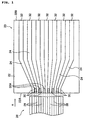
- Figure 1 is a front view showing a connector 20 for a narrow pitch preferred as a first embodiment and a terminal portion of a connection object 26 to which the connector is to be connected
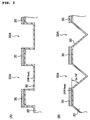
- Figures 2(A) and 2(B) are side views as seen from a direction indicated by an arrow A in Figure 1.
- the connector 20 for a narrow pitch preferred as the first embodiment has a configuration wherein metal wires 24 are arranged on a substrate 22 as shown in Figure 1.
- the substrate 22 is composed of a rectangular single-crystal silicon and manufactured by cutting a semiconductor wafer into a lattice shape. Disposed on a surface of the substrate are a plurality of metal wires 24 so as to cross the substrate 22. Furthermore, terminal electrodes 30 which can be overlapped with terminal electrodes 28 formed on the connection object 26 are formed at ends of the metal wires 24 at a side, that is, an edge 22A of the substrate 22 (the terminal electrodes 30 and the terminal electrodes 28 are formed at an identical pitch).
- terminal electrodes 32 which have the same number of electrodes as that of electrodes on a side of the terminal electrodes 30 are formed at a magnified width and a magnified pitch (magnified twice in Figure 1).
- the metal wires 24 disposed on the surface of the substrate 22 are configured to change a wiring width and a spacing between the wires in a section from the edge 22A to the edge 22B, and establish electrical conduction from the terminal electrodes 30 to the terminal electrodes 32.
- Grooves 33A are formed among the plurality of terminal electrodes 30 which are disposed at the edge 22A of the substrate 22.
- Figure 2(A) is an enlarged side view of the edge 22A of the connector 20 for a narrow pitch.
- An insulating film 50 is formed on a surface including the groove 33A of a single-crystal silicon 46 as shown in Figure 2(A).
- the metal wire 24 is disposed on the insulating film 50.
- the terminal electrodes 30 of the connection object are to be bonded to the terminal electrodes 28 of the connector 20 for a narrow pitch with an anisotropic electrically conductive adhesive which contains electrically conductive particles.
- the grooves 33A function as adhesive reservoirs which accommodate an excessive amount of the adhesive.
- a single-crystal silicon which has a crystal face to be exposed as a (110) face on a surface is to be used for composing the substrate 22.
- Use of the single-crystal silicon which has the crystal face to be exposed as the (110) face makes it possible to form the groove with extremely little undercut independently of a spacing between the terminal electrodes 30 adjacent to each other since the single-crystal silicon has a high crystal orientation in a direction perpendicular to an etching solution such as an aqueous solution of KOH or ethylenediamine (direction of depth of the terminal electrodes).
- a depth of the grooves 33A is set on the order of 100000 angstroms which is approximately three times of a particle diameter of the electrically conductive particles (approximately 30000 angstroms) to securely prevent the electrically conductive particles from being sandwiched between the terminal electrodes 30 adjacent to each other.
- the grooves 33A may have a V sectional shape as shown in Figure 2(B).
- a single-crystal silicon having a crystal face which is to be exposed on a surface as a (100) face is to be used for composing the substrate 22.
- Use of the single-crystal silicon having the crystal face which is to be exposed on the surface as the (100) face makes it possible to form the grooves 33A in the V shape at an angle of 54.74 degrees relative to the (100) face by anisotropically etching a surface of the single-crystal silicon using an etching solution such as an aqueous solution of KOH or ethylenediamine.
- a depth of the V-shaped grooves 33A can be accurately controlled dependently on a width of a window (made, for example, of an SiO 2 film) set on the (100) face.
- connection object 26 on which the terminal electrodes 28 are to be formed is, for example, a micro machine which uses a fine moving mechanism formed on a substrate and fine wires pulled out to apply a voltage to the moving mechanism.
- a piezoelectric actuator using a piezoelectric element, an electrostatic actuator using an electrostatic oscillator or the like is an example of the micro machine.
- connection object 26 will be described in detailed embodiments explained later.
- connection object 26 description will be made of procedures for connecting the connector 20 for a narrow pitch having the above described configuration to the connection object 26.
- Figure 3 is a diagram descriptive of the procedures for connecting the connection object 26 to the connector 20 for a narrow pitch
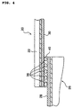
- Figure 4 is an enlarged view of a portion d in Figure 3
- Figures 5(A) and 5(B) are sectional views taken along a B-B line in Figure 3.
- connection object 26 When the connector 20 for a narrow pitch is to be connected to the connection object 26, the connection object 26 is placed on a top surface of a bonding stage 34 as shown in Figures 3, 4, 5(A) and 5(B). Disposed in the bonding stage 34 is a lower heater 36 so that the connection object 26 can be heated by operating the lower heater 36.
- the connector 20 is disposed so as to overlap the terminal electrodes 30 with the terminal electrodes 28.
- An anisotropic electrically conductive adhesive 40 which contains electrically conductive particles 38 is applied between the terminal electrodes 28 and the terminal electrodes 30 as shown in Figure 4 and the connector 20 is pressed from a side of a rear side surface to bring the electrically conductive particles 38 into contact with the terminal electrodes 28 and the terminal electrodes 30, thereby the terminal electrodes are conductive to each other by way of the electrically conductive particles 38.
- Hardening of the anisotropic electrically conductive adhesive 40 containing the electrically conductive particles 38 is accelerated by operating the lower heater 36 and a heater built in a bonding tool described later.
- a bonding tool 42 is disposed over the terminal electrodes 30, that is, over the connector 20 for a narrow pitch.
- the bonding tool 42 is attached to a linear guide (not shown) so that the bonding tool 42 itself can be raised and lowered along the linear guide.
- the connector 20 for a narrow pitch can be pressed from the side of the rear surface and the overlapped terminal electrodes 28 and terminal electrodes 30 can be brought into close contact with each other.
- An upper heater 44 is built in the bonding tool 42 so that a tip of the bonding tool 42 and the connector 20 for a narrow pitch can be heated by operating the upper heater 44.
- the upper heater 44 and the lower heater 36 are set so that a temperature will be uniform around a border line between the terminal electrodes 28 and the terminal electrodes 30, that is, so that no temperature difference is produced between the substrate 22 and the connection object 26 when the bonding tool 42 is lowered and a rear surface of the substrate 22 is pressed by the tip of the bonding tool 42. It is needless to say that the upper heater 44 and the lower heater 36 are set at a temperature which is sufficient at least for accelerating the hardening of the anisotropic electrically conductive adhesive 40.
- the terminal electrodes 28 are connected to the terminal electrodes 30 by lowering the bonding tool 42 so that the bonding tool 42 is set in the condition shown in Figure 5(B) from a condition shown in Figure 5(A). Since the substrate 22 and the connection object 26 are heated to an identical temperature with no temperature difference at this connecting stage, the substrate 22 and the connection object 26 which are made of an identical material are elongated at an identical ratio by heating and relative locations of the terminal electrodes 28 and the terminal electrodes 30 are not changed. Accordingly, the connector for a narrow pitch is capable of joining the terminal electrodes securely, or preventing a defect such as enhancement of a resistance value, improper joining or short circuit between the adjacent terminals from being caused at a time to connect the electrodes.
- Silicon is used as a material of the substrate 22 and the connection object 26 in the first embodiment described above and the inventor has confirmed by various examinations that the terminal electrodes can be connected securely even at a wiring pitch of 25 ⁇ m or narrower when silicon is used as the material (the terminal electrodes can be connected securely even at a wiring pitch on the order of 15 ⁇ m and the terminal electrodes are connectable even at a wiring pitch of 15 ⁇ m or narrower dependently on connecting resolution).
- the grooves 33A are formed among the plurality of terminal electrodes 30 in the first embodiment, an excessive amount of the anisotropic electrically conductive adhesive 40 applied to surfaces of the terminal electrodes 30 is moved toward the grooves 33A and the adhesive 40 containing the electrically conductive particles 38 is reserved in the grooves 33A as shown in Figure 6 when the terminal electrodes 28 are overlapped with the terminal electrodes 30. Since the grooves 33A which function as reservoirs for the anisotropic electrically conductive adhesive 40 is formed as described above, the electrically conductive particles 38 are not sandwiched between members other than the terminal electrodes 28 and the terminal electrodes 30. Accordingly, the connector 20 for a narrow pitch is capable of preventing adjacent terminal electrodes from being shorted by sandwiching the electrically conductive particles 38 between the adjacent terminal electrodes.
- the substrate 22 and the connection object 26 are made of an identical material in the first embodiment described above, the present invention is not limited by the embodiment. Even when these members are made of different materials and have different coefficients of thermal expansion, it is possible to securely join the substrate 22 with the connection object 26. In this case, a temperature difference is positively produced between the substrate 22 and the connection object 26 by changing output values from the upper heater 44 and the lower heater 36.
- a heater which is disposed on a side of a small coefficient of thermal expansion is set at a high temperature
- a heater which is set on a side of a large coefficient of thermal expansion is set at a low temperature.
- the first embodiment is an example where the depth of the grooves 33A is specified in relation to the diameter of the electrically conductive particles on a premise that the terminal electrodes 22 and 30 are bonded with the anisotropic electrically conductive adhesive or the anisotropic electrically conductive film.
- this specific method is insignificant when the terminal electrodes 22 and 30 are to be connected without using the anisotropic electrically conductive adhesive or the anisotropic electrically conductive film.
- the depth of the grooves 33A may therefore be determined in relation to a width of the groove. When the groove has a great width, for example, the grooves may have a shallow depth since the groove has a large spatial volume even when it has the shallow depth.
- the grooves When the grooves have a narrow width in contrast, the grooves must have an extensive depth so that it has a large spatial volume.
- a depth on the order of 5% to 150% of a groove width may be considered as a reference guide for the depth of the grooves 33A. Too great a depth of the grooves makes the terminal portion liable to fall down, thereby posing a problem in strength. From view points of strength and manufacturing facility, a depth on the order of 25% of a groove width is most preferable.
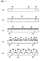
- Figures 7(a), 7(b), 7(c), 7(d), 7(e), 8(f), 8(g),8(h) and 8(i) are diagrams descriptive of manufacturing procedures for the connector 20 for a narrow pitch preferred as the first embodiment. These drawings show conditions of the metal wires 24 formed on the substrate 22 as seen from a direction indicated by an arrow A in Figure 1.
- Figure 7(a) shows a semiconductor wafer 46 made of single-crystal silicon on which the metal wires 24 are to be formed.
- Broken lines in Figure 7(a) indicate dicing lines 48 for separation from connectors 20 for a narrow pitch which are to be formed at adjacent locations.
- An insulating film 50 having thickness of 5000 to 20000 angstroms is formed on a surface of the semiconductor wafer 46 as shown in Figure 7(b).
- This insulating film 50 may be made, for example, of BPSG (boron-phospho-silicate glass) deposited by a CVD method or an oxide produced by dry thermal oxidation or wet thermal oxidation.
- BPSG boron-phospho-silicate glass
- a photoresist film 54 is coated over this oxide film as shown in Figure 7(c). Then, the insulating film 50 and the photoresist film 54 are patterned by carrying out exposure and development. Then, the oxide film is removed to expose a surface of the silicon as shown in Figure 7(d) for forming grooves. Furthermore, the resist is released by washing and grooves are formed as shown in Figure 7(e) by anisotropically etching the surface of the semiconductor wafer using an etching solution such as an aqueous solution of KOH, an aqueous solution of ethylenediamine or the like. Thereafter, an insulating film is formed on the surface of the semiconductor wafer as shown in Figure 8(f) by depositing the BPSG by the CVD method or producing the thermal oxide film by the dry thermal oxidation or the wet thermal oxidation.
- the semiconductor wafer on which the insulating film has been formed is placed in an argon atmosphere at a pressure of 2 to 5 mTorr and a temperature of 150 to 300°C.
- a metal film 52 is deposited to thickness of 200 to 20000 angstroms by sputtering with an input power of DC 9 to 12 kW for forming metal wires which have the same composition as that of the target ( Figure 8(g)).
- the metal film 52 may be formed by depositing Au to thickness on the order of 1000 angstroms on a base of Cr.
- a photoresist film 54 is coated as shown in Figure 8(h). Furthermore, metal wires are formed as shown in Figure 8(i) by etching the metal film 52 using as a mask the photoresist film which has been exposed and developed.
- the connector for a narrow pitch is cut out from the semiconductor wafer by carrying out a cutting work along the dicing lines.
- the metal wires are not left at all in the grooves in the first embodiment described above, the metal wires may be left in the grooves.
- the insulating film 50 is patterned while adjusting exposure so as to leave the resist film 54 on bottoms of the grooves as shown in Figure 9(a) after coating the resist film 54 as shown in Figure 8(h).
- the metal wires can be left on the bottoms of the grooves as shown in Figure 9(b) by carrying out etching in a condition where the resist film 54 is left on the bottoms of the grooves.
- the resist When the grooves are deep, the resist is to be coated by spraying and a resist, or an electrodeposition resist to form the resist film 54 before coating the resist film 54 shown in Figure 8(h) and patterned by exposing the resist to projected rays.
- the resist By patterning the resist as described above, it is possible to obtain a substrate of a good quality which is scarcely troubled or defective by short circuit or wire breakage.
- the metal wires left on the bottoms of the grooves enhance bonding strength at a step of bonding the connection object to the connector for a narrow pitch.
- Enhanced bonding strength provides connection having high resistance to humidity.
- each of the first embodiment and the second embodiment is configured to completely insulate the groove from the single-crystal silicon with the insulating film
- the third embodiment is configured not only to leave a metal wire on the bottom of the grooves but also to make the metal wire conductive to a single-crystal silicon plate and connect the metal wire in the groove to a ground wiring portion (negative electrode) or a power source wiring portion (positive electrode).
- the metal wire By disposing the metal wire as described above, it is possible to set the single-crystal silicon plate at a potential identical to that of the ground wiring portion (negative electrode) or the power source wiring portion (positive electrode), thereby stabilizing the potential of the single-crystal silicon plate.
- the metal wire after it is formed or control a resistivity of a single-crystal silicon plate to be used to 0.3 ⁇ cm or lower in order to improve adhesion of the metal wire formed in the groove to the single-crystal silicon plate and an ohmic contact.
- Such heating or control makes it possible to prevent an element from operating erroneously due to line noise in a fine wiring portion.
- the heating or control makes it possible to reduce radiation noise by a function of electrostatic shielding.
- a groove is formed in the single-crystal silicon plate as shown in Figure 8(f) descriptive of the first embodiment and after forming an insulating film, the insulating film is partially removed from the bottom of the groove as shown in Figure 10(a) by etching with fluorine.
- a metal film is deposited as shown in Figure 10(b) for forming a metal wire.
- a resist film is coated and patterned as shown in Figure 10(c). By etching the resist film in this condition, the metal wire can be left on the bottom of the groove and made conductive to the single-crystal silicon plate as shown in Figure 10(d).
- the insulating film 50 may not be formed in the groove 33A.
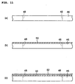
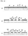
- Figures 11(a), 11(b), 11(c), 12(d), 12(e) and 12(f) are diagrams descriptive of procedures for manufacturing a connector 20 for a narrow pitch wherein the insulating film 50 is not formed in grooves 33A.
- Figure 11(a) shows a semiconductor wafer 46 made of single-crystal silicon on which the metal wires 24 are to be formed.
- Broken lines in Figure 11(a) indicate dicing lines 48 for separating the connector 20 for a narrow pitch from those formed at adjacent locations.
- the semiconductor wafer 46 on which the insulating film 50 is disposed is placed in an argon atmosphere at a pressure of 2 to 5 mTorr and a temperature of 150 to 300°C, and a metal film 52 is deposited to thickness of 200 to 20000 angstroms by sputtering with an input power of DC 9 to 12 kW using Al-Cu, Al-Si-Cu, Al-Si, Ni, Cr, Au or the like as a target, thereby forming metal wires 24 which have a composition identical to that of the target.
- the metal film 52 may be formed by depositing Au to thickness on the order of 1000 angstroms on a base of Cr. This condition is shown in Figure 11(c).
- grooves 33A are formed on both sides of the metal wires 24 (terminal electrodes 30) by anisotropically etching the surface of the semiconductor wafer 46 as shown in Figure 12(f) using an etching solution such as an aqueous solution of KOH or an aqueous solution of ethylenediamine.
- an etching solution such as an aqueous solution of KOH or an aqueous solution of ethylenediamine.
- Figure 13 is a diagram descriptive of a connector for a narrow pitch preferred as a fifth embodiment.
- members which are the same as or correspond to those in the first embodiment are represented by the same reference numerals.
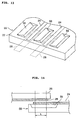
- a connector 55 for a narrow pitch preferred as the fifth embodiment is configured so that grooves 56 formed at an end is not extended to an end of the connector as shown in Figure 13.
- the grooves 56 are set at a length which is longer than a connection range L as shown in Figure 14.
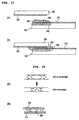
- a space enclosed by a connection object and the connector for a narrow pitch constitutes an enclosed space. Accordingly, air may be involved and air bubbles 57 may remain in the enclosed space when an adhesive 40 is coated and the connection object 26 is joined to a connector 55A for a narrow pitch as shown in Figure 15. The remaining air bubbles 57 may be swollen and contracted by an environmental changes (temperature changes), thereby producing an adverse influence on a connected condition. Even when air bubbles do not remain, incomplete discharge of the adhesive 40 may allow an internal pressure to remain in a groove 56A as shown in Figure 16(A) and function to release bonding after the adhesive is hardened.
- the internal pressure may degrade bonding of an electrically conductive particle 38 to two terminal electrodes 24 and 28 as shown in Figure 16(B).
- the length of the groove 56A which is shorter than the connection range L as described above poses a problem that the connection is made incomplete under an influence due to the air bubbles 57 or the internal pressure.
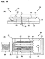
- the electrostatic actuator 59 shown in Figures 19(A) and 19(B) is an actuator which is configured for use in an ink head of an ink jet printer and has a micro structure formed by micro working according to the micro machining technology.
- an ink jet head consists of an ink jet head main unit 60 and a connector unit 88 for external wiring which are manufactured separately and connected to each other.
- the ink jet head main unit 60 has a three-layer structure composed by laminating a silicon substrate 70, an upper side nozzle plate 72 which is made also of silicon and a lower side glass substrate 74 which is made of borosilicate glass as shown in Figure 19(A).
- a common ink chamber 78 Disposed in the middle silicon substrate 70 are five independent ink chambers 76, a common ink chamber 78 which connects the five ink chambers 76 and a groove which functions as an ink supply path 80 communicating with the common ink chamber 78 and the ink chambers 76.
- the groove is closed with a nozzle plate 72, thereby partitioning and forming the ink chambers 76 and the supply paths 80.
- each concavities is formed on a rear side of the silicon substrate 70 at locations corresponding to the ink chambers 76 and closed with the glass substrate 74, thereby forming an oscillation chamber 71 having a height indicated by a size q in Figure 19(A).
- Partition walls of the ink chambers 76 and the oscillation chamber 71 of the silicon substrate 70 are configured as oscillating plates 66 which function as elastically deformable oscillators.
- Nozzles 62 are formed in the nozzle plate 72 at locations corresponding to tips of the ink chambers 76 and communicating with the ink chambers 76.
- the grooves disposed in the silicon substrate 70 and the nozzles 62 disposed in the nozzle plate 72 are formed using the micro working technique according to the micro machining technology.
- Opposed electrodes 90 which are opposed to each other are disposed on the oscillating plates 66 and the glass substrate 74.
- Fine gaps formed between the silicon substrate 70 and the opposed electrodes 90 are sealed with sealing members 84.
- the opposed electrodes 90 on the glass substrate 74 are pulled out on a left side in Figures 19(A) and 19(B) to form terminal electrode 86.
- a connector 88 for a narrow pitch which is manufactured separately is connected to the terminal electrodes 86, thereby composing the ink jet head having a connector section.
- the plurality of ink jet head main units 60 which have the configuration described above are manufactured in a condition of a wafer and cut out along dicing lines. After dicing, the ink jet head main unit 60 is connected to the connector 88 for a narrow pitch which is manufactured separately.
- the sixth embodiment is configured to manufacture the ink jet head main unit 60 and the connector 88 for a narrow pitch separately and join these members to each other, the sixth embodiment provides an effect which will be described below.
- the ink jet head main unit 60 is manufactured by laminating the glass substrate 74, the silicon substrate 70 and the nozzle plate 72 in a condition of a wafer as described above.
- the terminal electrodes 86 are formed on the glass substrate 74 for external electrical connection, and extended outward from the silicon substrate 70 and the nozzle plate 72. Accordingly, the wafer on which the silicon substrate 70 or the nozzle plate 72 is disposed at a location opposed to the terminal electrodes 86 is not utilized at a laminating step.
- the ink jet head main unit 60 itself can be electrically connected to an external substrate, it will be necessary to dispose terminal electrodes at a wide pitch on the glass substrate 74 so as to permit external wiring, whereby the terminal electrodes 86 will be rather large.
- the large terminal electrodes 86 are formed on the glass substrate 74, the wafer on which the silicon substrate 70 or the nozzle plate 72 is formed at the location opposed to the terminal electrodes 86 is not utilized, thereby wasting the wafer having a large area.
- highly pure and expensive silicon crystal plates must be used to form the oscillating plates 66 which are remarkably thin (approximately 1 ⁇ m) on the silicon substrate 70. A manufacturing cost of a product is largely influenced by wasting the expensive silicon crystal plates.
- the sixth embodiment permits configuring a terminal portion of the ink jet head main unit 60 compact, thereby not wasting expensive silicon crystal plates. Moreover, the sixth embodiment makes it possible to lower a manufacturing cost of an apparatus as a whole since a silicon crystal plate used to form the connector 88 for a narrow pitch does not need to have a purity so high as that of silicon crystal plates used to form the oscillating plates 66.
- FIG 20 is a diagram descriptive of a piezoelectric actuator preferred as a seventh embodiment.
- a piezoelectric actuator 91 comprises a piezoelectric oscillator 93 which has external electrodes 93a and 93b formed on both sides, and a holding member 95 which holds the piezoelectric oscillator 93.
- a protruding portion 97 is formed on the holding member 95 and the piezoelectric oscillator 93 is joined to the holding member 95 at a joining area A of the protruding portion 97.
- the external electrodes 93a and 93b (portions traced in thick lines in the figure) of the piezoelectric oscillator 93 extend from both side surfaces to middles locations of first surfaces 93c respectively.
- Electrodes 95a and 95b which are formed on the holding member 95 and traced in thick lines also extend from both outside edges to a middle of the protruding portion 97.
- the piezoelectric oscillator 93 is rigidly joined to the holding member 95 at the joining area A set on the protruding portion 97, and the external electrodes 93a and 93b of the piezoelectric oscillator 93 are connected and made conductive to the electrodes 95a and 95b of the holding member.
- a connector 20 for a narrow pitch is connected to the electrodes 95a and 95b of the holding member 95 so that an external signal is input into the piezoelectric actuator 91 from outside by way of the connector 20 for a narrow pitch.
- FIG 21 is a conceptional diagram showing an ink jet head 98 which uses the piezoelectric actuator 91 shown in Figure 20.
- a nozzle plate 108 having a nozzle 101 is joined to a tip of an ink flow path 99 which is composed of a flow path forming member 103 and an oscillating plate 105, and an ink supply path 108 is disposed at an end on an opposite side.
- the piezoelectric actuator 91 is disposed so that a mechanical function surface 93d is kept in contact with an oscillating plate 95 and opposed to the ink flow path 99.
- the external electrodes 93a and 93b on both the sides of the piezoelectric oscillator 93 are connected to the electrodes 95a and 95b of the holding member, and external signals are input into the piezoelectric actuator 91 by way of the electrodes 95a and 95b of the holding member 95 as well as the connector 20 for a narrow pitch.
- the mechanical function surface 93d causes swelling deformation and deflecting deformation at the same time with a high efficiency, thereby gaining a very large effective displacement in a vertical direction in Figure 21. Due to this deformation, the oscillating plate 95 is deformed in correspondence with the mechanical function surface 93d as indicated by dotted lines in Figure 21, thereby producing a large pressure change (volume change) in the ink flow path 99.
- This pressure change causes ink ejection from the nozzle 101 in a direction indicated by an arrow in Figure 21 and the ink ejection is remarkably efficient since the pressure change is remarkably efficient.
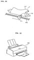
- the ink jet head 98 preferred as the eighth embodiment described above is used in a condition where it is mounted on a carriage 111 as shown in Figure 22.
- the carriage 111 is movably mounted on a guide rail 113 and a location of the carriage 111 is controlled in a direction of width of paper 117 which is fed out by a roller 115.
- a mechanism shown in Figure 22 is disposed in an ink jet printer 119 shown in Figure 23.
- the ink jet head 98 can be used as a line head of a line printer. In such a case, the carriage 111 is unnecessary.
- an ink jet printer may have a similar configuration when the ink jet printer uses an ink jet head 60 of a type which ejects an ink drop from a side of a face surface using the electrostatic actuator mentioned in the seventh embodiment described above.
- Figures 24(A) and 24(B) show a micro pump as an example of a micro machine preferred as a tenth embodiment: Figure 24(A) being a top view of the micro machine and Figure 24(B) being sectional view of the micro machine.
- the micro pump operates on a principle that it changes a pressure in a pressure chamber 128 by applying a voltage to a piezoelectric element 127 bonded to a diaphragm 126 formed at a center location of the silicon substrate 121 and deflecting the diaphragm, and opens and closes a suction valve 132 and an ejection valve 133 by displacing a suction side diaphragm 129 and an ejection side diaphragm 131 which are spatially continuous to the pressure chamber 128, thereby feeding the fluid under pressure from the suction side pipe 124 into the ejection side pipe 125.
- the pressure chamber 128 is spatially continuous to a space over the suction side diaphragm 129 and a space under the ejection side diaphragm 131.
- wiring is made to an outside by way of the connector for a narrow pitch according to the present invention as in the sixth through eighth embodiments described above.
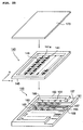
- Figure 25 is an exploded perspective view showing main parts of a light modulator preferred as another embodiment of the present invention.
- the light modulator is configured mainly by a silicon substrate 140, a glass substrate 150 and a cover substrate 170.
- the silicon substrate 140 has a plurality of fine mirrors 141 which are arranged on a matrix. Out of the plurality of fine mirrors 141, fine mirrors 141 which are arranged in a direction, for example an X direction in Figure 25, are connected with torsion bars 143. Furthermore, a frame like member 145 is disposed so as to surround a region at which the plurality of fine mirrors 141 are arranged. Connected to this frame like member 145 are ends of the plurality of torsion bars 143. Furthermore, slits are formed in the fine mirrors 141 around portions connected to the torsion bars 143 to facilitate inclining drive of the torsion bars 143 in a direction around axial lines.
- reflecting layers 141a are formed on surfaces of the fine mirrors 141.
- a reflecting direction of rays incident on the fine mirrors 141 is changed.
- Light can be modulated by controlling a time period for which the rays are reflected in a predetermined direction.
- a circuit which incliningly drives the fine mirrors 141 is disposed on the glass substrate 150.
- the glass substrate 150 has concavities 151 at a central region and a rising member 153 formed around the concavities. A portion of the rising member 153 is notched to form an electrode withdrawal port 155 and an electrode withdrawal plate portion 157 which is continuous to the concavities 151 is formed outside the electrode withdrawal port 155.
- the glass substrate 150 has a large number of support members 159 which are formed in the concavities 151 so as to protrude from the concavities 151 to a height of a ceiling of the rising member 153 at locations opposed to the torsion bars 143 between the two fine mirrors 141 adjacent to one another in the X direction.
- a wiring pattern 161 is formed on the concavities 151 and the electrode withdrawal plate portion 157 of the glass substrate 150.
- This wiring pattern 161 has first and second address electrodes 163 and 165 at locations opposed to rear surfaces of the fine mirrors 141 on both sides of the torsion bars 143.
- the first address electrodes 163 which are arranged in the Y direction are connected commonly to a first common wire 167.
- the second address electrodes 165 which are arranged in the Y direction are connected commonly to a second common wire 169.
- the silicon substrate 140 is anodically joined on the glass substrate 150 which has a configuration described above. At this time, both the ends of the torsion bars 143 and the frame like member 145 of the silicon substrate 140 are joined to the rising member 153 of the glass substrate 150. Furthermore, intermediate portions of the torsion bars 143 of the silicon substrate 140 are anodically joined to the support members 159 of the glass substrate 150, Thereafter, the cover substrate 170 is joined over the frame like member 145 of the silicon substrate 140. Both ends of each torsion bar 143 which are coupled with the frame like member 145 are diced at locations to be cut off the frame like member 145. Furthermore, a circumferential edge portion including the electrode withdrawal port 155 notched in the rising member 153 of the glass substrate 150 is sealed and enclosed with a sealing agent, thereby completing the light modulator.
- the first common wire 167 and the second common wire 169 of the completed light modulator are connected to a flexible substrate such as a tape carrier package incorporated with a drive IC by way of the connector for a narrow pitch according to the present invention as in the sixth through eighth embodiments described above so that external signals are input into the light modulator.
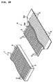
- FIG. 26 is a diagram descriptive of an example of a liquid crystal panel preferred as a twelfth embodiment of the present invention in a condition of a module step after completing an array step and a cell step, that is, a condition before an electronic circuit and the like of a drive system is disposed so that a liquid crystal cell can be electrically controlled.
- a liquid crystal panel 180 has a liquid crystal cell 181, a connector 182 for a narrow pitch and a tape carrier package 184 incorporated with a drive IC 183.
- the liquid crystal cell 181 is configured, for example, by two substrates 181a and 181b between which a liquid crystal material is injected and enclosed: pixel electrodes, a thin film transistor connected to the pixel electrodes, a source for the thin film transistor, a source line electrically connected to a gate, a data line and the like are formed on the substrate 181a (located upper in Figure 26), whereas opposed electrodes, color filters and the like are disposed on the substrate 181b (located lower in Figure 26).
- terminal electrodes 185 formed on the liquid crystal cell 181 are overlapped with terminal electrodes 186 of the connector 182 for a narrow pitch or the terminal electrodes 185 are overlapped with the electrode terminals 186 at a narrow pitch with an electrically conductive member interposed, and connected to each other by pressurizing and heating.
- terminals 187 disposed at an end of a wiring pattern which enlarges and extends from other ends of the terminal electrodes 186 at the narrow pitch of the connector 182 for a narrow pitch are connected to terminals 188 of the tape carrier package 184, thereby making the terminal electrodes 185 conductive to the drive IC 183.
- the connector 182 for a narrow pitch When the connector 182 for a narrow pitch is disposed as described above, it is possible to minimize an area of the liquid crystal cell 181 to be occupied by the terminal electrodes 185. A large display section can therefore be reserved even with a liquid crystal cell which has an area remaining unchanged from a conventional area. Furthermore, the invention makes it possible to connect the terminal electrodes at a narrow pitch, thereby increasing the number of terminals in a connecting section. Accordingly, it is possible to arrange wires and pixels at narrow pitches with high precision.
- Figure 27 shows a portable telephone as an example of electronic appliance which utilizes the liquid crystal panel preferred as the twelfth embodiment.
- the liquid crystal panel is used in a display member 191 of a portable telephone 190 shown in Figure 27.
Landscapes
- Engineering & Computer Science (AREA)
- Physics & Mathematics (AREA)
- Microelectronics & Electronic Packaging (AREA)
- Manufacturing & Machinery (AREA)
- Nonlinear Science (AREA)
- General Physics & Mathematics (AREA)
- Optics & Photonics (AREA)
- Crystallography & Structural Chemistry (AREA)
- Chemical & Material Sciences (AREA)
- Mathematical Physics (AREA)
- Computer Hardware Design (AREA)
- Particle Formation And Scattering Control In Inkjet Printers (AREA)
- Coupling Device And Connection With Printed Circuit (AREA)
- Combinations Of Printed Boards (AREA)
- Liquid Crystal (AREA)
- Accessory Devices And Overall Control Thereof (AREA)
Abstract
Description
Claims (20)
- A narrow pitch connector comprising a plurality of first terminal electrodes and a plurality of second terminal electrodes which are formed on a substrate, and wires formed thereon for electrically connecting said first terminal electrodes with said second terminal electrodes: said wires having a function of making conversion from a pitch of said first terminal electrodes to a pitch of said second terminal electrodes, characterized in that grooves are formed between said first terminal electrodes respectively.
- The narrow pitch connector according to claim 1, characterized in that an insulating film is formed in said grooves.
- The narrow pitch connector according to claim 2, characterized in that metal wires are formed on the insulating film formed in said grooves.
- The narrow pitch connector according to claim 3, characterized in that the metal wires are connected to said substrate and a ground wiring portion or a power source wiring portion.
- The narrow pitch connector according to any one of claims 1 through 4, characterized in that said first terminal electrodes are electrodes to be electrically connected to external terminal electrodes formed on a connection object and said grooves are formed to reserve an adhesive used to connect said first terminal electrodes with said external terminal electrodes.
- The narrow pitch connector according to claim 5, characterized in that a depth of said grooves is set not shallower than three times of a particle diameter of electrically conductive particles contained in said adhesive.
- The narrow pitch connector according to any one of claims 1 through 6, characterized in that said groove is set longer than an overlapped portion of the terminal electrodes.
- The narrow pitch connector according to claim 5, characterized in that said narrow pitch connector has characteristic that a coefficient of thermal expansion of said substrate is nearly equal to a coefficient of thermal expansion of said connection object or smaller than the coefficient of thermal expansion of said connection object.
- The narrow pitch connector according to any one of claims 1 through 8, characterized in that said substrate is made of single-crystal silicon.
- The narrow pitch connector according to claim 9, characterized in that a crystal face of said single-crystal silicon is a (100) face.
- The narrow pitch connector according to claim 9, characterized in that a crystal face of said single-crystal silicon is a (110) face.
- A micro machine, comprising a moving mechanism portion and a first substrate on which a plurality of first terminal electrodes are formed, characterized in that:said micro machine comprises a second substrate on which second terminal electrodes are formed to be electrically connected to said plurality of first terminal electrodes;a plurality of third terminal electrodes and wires for electrically connecting said second terminal electrodes with said third terminal electrodes are formed on said second substrate;said wires have a function of making conversion from a pitch of said second terminal electrodes to a pitch of said third terminal electrodes; andgrooves are formed between said second terminal electrodes respectively.
- A piezoelectric actuator comprising a piezoelectric element and a first substrate on which a plurality of first terminal electrodes are formed, characterized in that:said actuator comprises a second substrate on which second terminal electrodes are formed to be electrically connected to said plurality of first terminal electrodes;a plurality of third terminal electrodes and wires for electrically connecting said second terminal electrodes with said third terminal electrodes are formed on said second substrate;said wires have a function of making conversion from a pitch of said second terminal electrodes to a pitch of said third terminal electrodes; andgrooves are formed between said second terminal electrodes respectively.
- An electrostatic actuator comprising an electrostatic oscillator and a first substrate on which a plurality of first terminal electrodes are formed, characterized in that:said actuator comprises a second substrate on which second terminal electrodes are formed to be electrically connected to said plurality of first terminal electrodes;a plurality of third terminal electrodes and wires for electrically connecting said second terminal electrodes with said third terminal electrodes are formed on said second substrate;said wires have a function of making conversion from a pitch of said second terminal electrodes to a pitch of said third terminal electrodes; andgrooves are formed between said second terminal electrodes respectively.
- An ink jet head comprising a piezoelectric element and a first substrate on which a plurality of first terminal electrodes are formed, and functioning to eject an ink drop with said piezoelectric element, characterized in that:said ink jet head comprises a second substrate on which second terminal electrodes are formed to be electrically connected to said plurality of first terminal electrodes;a plurality of third terminal electrodes and wires for electrically connecting said second terminal electrodes with said third terminal electrodes are formed on said second substrate;said wires have a function of making conversion from a pitch of said second terminal electrodes to a pitch of said third terminal electrodes; andgrooves are formed between said second terminal electrodes respectively.
- An ink jet head comprising an electrostatic oscillator and a first substrate on which a plurality of first terminal electrodes are formed, and functioning to eject an ink drop with said electrostatic oscillator, characterized in that:said ink jet head comprises a second substrate on which second terminal electrodes are formed to be electrically connected to said plurality of first terminal electrodes;a plurality of third terminal electrodes and wires for electrically connecting said second terminal electrodes with said third terminal electrodes are formed on said second substrate;said wires have a function of making conversion from a pitch of said second terminal electrodes to a pitch of said third terminal electrodes; andgrooves are formed between said second terminal electrodes respectively.
- An ink jet printer comprising an ink jet head which comprises a piezoelectric element and a first substrate on which a plurality of first terminal electrodes are formed, characterized in that:said ink jet head comprises a second substrate on which second terminal electrodes are formed to be electrically connected to said plurality of first terminal electrodes;a plurality of third terminal electrodes and wires for electrically connecting said second terminal electrodes with said third terminal electrodes are formed on said second substrate;said wires have a function of making conversion from a pitch of said second terminal electrodes to a pitch of said third terminal electrodes; andgrooves are formed between said second terminal electrodes respectively.
- An ink jet printer comprising an ink jet head which comprises an electrostatic oscillator and a first substrate on which a plurality of first terminal electrodes are formed, characterized in that:said ink jet head comprises a second substrate on which second terminal electrodes are formed to be electrically connected to said plurality of first terminal electrodes;a plurality of third terminal electrodes and wires for electrically connecting said second terminal electrodes with said third terminal electrodes are formed on said second substrate;said wires have a function of making conversion from a pitch of said second terminal electrodes to a pitch of said third terminal electrodes; andgrooves are formed between said second terminal electrodes respectively.
- A liquid crystal device comprising a liquid crystal sandwiched between a first substrate and a second substrate as well as a plurality of first terminal electrodes formed on either of said first substrate and said second substrate, characterized in that:said liquid crystal device further comprises a third substrate on which second terminal electrodes are formed to be electrically connected to said first terminal electrodes;a plurality of third terminal electrodes and wires for electrically connecting said second terminal electrodes with said third terminal electrodes are formed on said third substrate;said wires have a function of making conversion from a pitch of said second terminal electrodes to a pitch of said third terminal electrodes; andgrooves are formed between said second terminal electrodes respectively.
- An electronic appliance comprising a liquid crystal device, characterized in that:said liquid crystal device comprises a first substrate, a second substrate, a liquid crystal sandwiched between the first substrate and the second substrate, and a plurality of first terminal electrodes formed on either of said first substrate and said second substrate;said liquid crystal device further comprises a third substrate on which second terminal electrodes are formed to be electrically connected to said plurality of first terminal electrodes;a plurality of third terminal electrodes and wires for electrically connecting said second terminal electrodes with said third terminal electrodes are formed on said third substrate;said wires have a function of making conversion from a pitch of said second terminal electrodes to a pitch of said third terminal electrodes; andgrooves are formed between said second terminal electrodes respectively.
Applications Claiming Priority (3)
| Application Number | Priority Date | Filing Date | Title |
|---|---|---|---|
| JP9407299 | 1999-03-31 | ||
| JP9407299 | 1999-03-31 | ||
| PCT/JP2000/002071 WO2000058205A1 (en) | 1999-03-31 | 2000-03-31 | Narrow-pitch connector, electrostatic actuator, piezoelectric actuator, ink-jet head, ink-jet printer, micromachine, liquid crystal panel, and electronic apparatus |
Publications (3)
| Publication Number | Publication Date |
|---|---|
| EP1092676A1 true EP1092676A1 (en) | 2001-04-18 |
| EP1092676A4 EP1092676A4 (en) | 2002-06-05 |
| EP1092676B1 EP1092676B1 (en) | 2008-01-02 |
Family
ID=14100310
Family Applications (1)
| Application Number | Title | Priority Date | Filing Date |
|---|---|---|---|
| EP00913017A Expired - Lifetime EP1092676B1 (en) | 1999-03-31 | 2000-03-31 | Narrow-pitch connector, electrostatic actuator, piezoelectric actuator, ink-jet head, ink-jet printer, micromachine, liquid crystal panel, and electronic apparatus |
Country Status (8)
| Country | Link |
|---|---|
| US (1) | US6601947B1 (en) |
| EP (1) | EP1092676B1 (en) |
| JP (1) | JP4023089B2 (en) |
| KR (1) | KR100465444B1 (en) |
| CN (1) | CN1298612C (en) |
| DE (1) | DE60037627T2 (en) |
| TW (1) | TW456075B (en) |
| WO (1) | WO2000058205A1 (en) |
Cited By (1)
| Publication number | Priority date | Publication date | Assignee | Title |
|---|---|---|---|---|
| EP2084786A4 (en) * | 2006-10-25 | 2010-01-20 | 3M Innovative Properties Co | Method of connecting circuit boards and connected structure |
Families Citing this family (23)
| Publication number | Priority date | Publication date | Assignee | Title |
|---|---|---|---|---|
| JP4653374B2 (en) * | 2001-08-23 | 2011-03-16 | セイコーエプソン株式会社 | Manufacturing method of electro-optical device |
| US7334871B2 (en) * | 2004-03-26 | 2008-02-26 | Hewlett-Packard Development Company, L.P. | Fluid-ejection device and methods of forming same |
| TWI351670B (en) * | 2006-05-18 | 2011-11-01 | Au Optronics Corp | Signal transmission assembly and display panel app |
| JP4715778B2 (en) * | 2007-03-08 | 2011-07-06 | ブラザー工業株式会社 | Inkjet head manufacturing method |
| CN101784952A (en) * | 2007-06-20 | 2010-07-21 | 株式会社普利司通 | Information display panel |
| JP4683026B2 (en) | 2007-09-07 | 2011-05-11 | Tdk株式会社 | Common mode choke coil and manufacturing method thereof |
| US8348393B2 (en) * | 2008-03-17 | 2013-01-08 | Hewlett-Packard Development Company, L.P. | Print head diaphragm support |
| JP2011096823A (en) * | 2009-10-29 | 2011-05-12 | Panasonic Corp | Board connection structure |
| CN103367947A (en) * | 2012-04-10 | 2013-10-23 | 宸鸿科技(厦门)有限公司 | Connection structure |
| US9116022B2 (en) | 2012-12-07 | 2015-08-25 | Analog Devices, Inc. | Compact sensor module |
| WO2015083364A1 (en) * | 2013-12-02 | 2015-06-11 | 東芝ホクト電子株式会社 | Light-emission device |
| JP2015128863A (en) * | 2014-01-08 | 2015-07-16 | セイコーエプソン株式会社 | WIRING BOARD, DROPLET DISCHARGE HEAD, PRINTING APPARATUS, ELECTRONIC DEVICE, AND WIRING BOARD MANUFACTURING METHOD |
| JP6604035B2 (en) * | 2015-05-27 | 2019-11-13 | ブラザー工業株式会社 | Liquid ejection device and method of manufacturing liquid ejection device |
| KR102403671B1 (en) | 2015-09-18 | 2022-05-27 | 엘지디스플레이 주식회사 | Display Device |
| KR102372209B1 (en) * | 2015-12-03 | 2022-03-08 | 삼성디스플레이 주식회사 | Display device |
| JP6915250B2 (en) * | 2016-09-28 | 2021-08-04 | ブラザー工業株式会社 | Connection structure of actuator device, liquid discharge device, and wiring member |
| JP6904238B2 (en) * | 2017-12-19 | 2021-07-14 | 住友電気工業株式会社 | Multi-core cable with connecting member |
| KR102757145B1 (en) | 2018-12-06 | 2025-01-21 | 아나로그 디바이시즈 인코포레이티드 | Shielded integrated device packages |
| US11688709B2 (en) | 2018-12-06 | 2023-06-27 | Analog Devices, Inc. | Integrated device packages with passive device assemblies |
| EP4012842A4 (en) | 2019-08-09 | 2023-08-02 | Sekisui Polymatech Co., Ltd. | CONNECTION COMPONENT AND CONNECTION STRUCTURE |
| JP7427969B2 (en) * | 2020-01-22 | 2024-02-06 | セイコーエプソン株式会社 | Electro-optical devices and electronic equipment |
| US11664340B2 (en) | 2020-07-13 | 2023-05-30 | Analog Devices, Inc. | Negative fillet for mounting an integrated device die to a carrier |
| JP7517020B2 (en) * | 2020-09-23 | 2024-07-17 | セイコーエプソン株式会社 | Piezoelectric drive device and robot |
Family Cites Families (10)
| Publication number | Priority date | Publication date | Assignee | Title |
|---|---|---|---|---|
| JPS57158824A (en) * | 1981-03-27 | 1982-09-30 | Nippon Sheet Glass Co Ltd | Optical connector |
| JPS598384A (en) | 1982-07-07 | 1984-01-17 | Nippon Telegr & Teleph Corp <Ntt> | Silicon wiring substrate |
| JPH0440277Y2 (en) | 1986-11-20 | 1992-09-21 | ||
| US4871319A (en) * | 1988-12-21 | 1989-10-03 | Amp Incorporated | Molded circuit board for ribbon cable connector |
| JP2633680B2 (en) | 1989-03-29 | 1997-07-23 | 株式会社リコー | Conductive pattern connector and its connection method |
| KR940006185Y1 (en) | 1990-06-07 | 1994-09-10 | 가시오 게이상기 가부시끼가이샤 | IC module |
| JPH0775177B2 (en) | 1992-05-06 | 1995-08-09 | カシオ計算機株式会社 | Junction structure |
| JPH06333652A (en) | 1993-05-24 | 1994-12-02 | Sumitomo Electric Ind Ltd | Terminal pitch converting connector for electronic parts |
| JPH10193596A (en) | 1997-01-09 | 1998-07-28 | Matsushita Electric Ind Co Ltd | Inkjet recording head |
| EP0860279B1 (en) * | 1997-02-21 | 2002-05-22 | Seiko Epson Corporation | Ink jet recording head |
-
2000
- 2000-03-31 WO PCT/JP2000/002071 patent/WO2000058205A1/en not_active Ceased
- 2000-03-31 TW TW089106108A patent/TW456075B/en not_active IP Right Cessation
- 2000-03-31 CN CNB008004757A patent/CN1298612C/en not_active Expired - Fee Related
- 2000-03-31 JP JP2000607918A patent/JP4023089B2/en not_active Expired - Fee Related
- 2000-03-31 EP EP00913017A patent/EP1092676B1/en not_active Expired - Lifetime
- 2000-03-31 KR KR10-2000-7013538A patent/KR100465444B1/en not_active Expired - Fee Related
- 2000-03-31 US US09/701,345 patent/US6601947B1/en not_active Expired - Lifetime
- 2000-03-31 DE DE60037627T patent/DE60037627T2/en not_active Expired - Lifetime
Cited By (1)
| Publication number | Priority date | Publication date | Assignee | Title |
|---|---|---|---|---|
| EP2084786A4 (en) * | 2006-10-25 | 2010-01-20 | 3M Innovative Properties Co | Method of connecting circuit boards and connected structure |
Also Published As
| Publication number | Publication date |
|---|---|
| WO2000058205A1 (en) | 2000-10-05 |
| CN1298612C (en) | 2007-02-07 |
| EP1092676B1 (en) | 2008-01-02 |
| JP4023089B2 (en) | 2007-12-19 |
| EP1092676A4 (en) | 2002-06-05 |
| KR20010043951A (en) | 2001-05-25 |
| DE60037627T2 (en) | 2008-12-11 |
| DE60037627D1 (en) | 2008-02-14 |
| HK1037594A1 (en) | 2002-02-15 |
| US6601947B1 (en) | 2003-08-05 |
| KR100465444B1 (en) | 2005-01-13 |
| CN1297421A (en) | 2001-05-30 |
| TW456075B (en) | 2001-09-21 |
Similar Documents
| Publication | Publication Date | Title |
|---|---|---|
| EP1092676B1 (en) | Narrow-pitch connector, electrostatic actuator, piezoelectric actuator, ink-jet head, ink-jet printer, micromachine, liquid crystal panel, and electronic apparatus | |
| JP4051884B2 (en) | Manufacturing method of semiconductor device, connector for narrow pitch, electrostatic actuator, piezoelectric actuator, inkjet head, inkjet printer, micromachine, liquid crystal device, electronic device | |
| JPWO2000059050A1 (en) | Semiconductor device manufacturing method, semiconductor device, narrow pitch connector, electrostatic actuator, piezoelectric actuator, inkjet head, inkjet printer, micromachine, liquid crystal panel, electronic device | |
| JPWO2000058205A1 (en) | Narrow pitch connectors, electrostatic actuators, piezoelectric actuators, inkjet heads, inkjet printers, micromachines, liquid crystal panels, electronic devices | |
| EP0732208B1 (en) | Ink jet print head having ceramic ink pump member and metallic nozzle member bonded thereto | |
| EP0738599B1 (en) | Ink Jet recording head and method of producing same | |
| KR100795212B1 (en) | Microdrop Precipitator | |
| KR100402871B1 (en) | Method of connecting electrode, narrow pitch connector, pitch changing device, micromachine, piezoelectric actuator, electrostatic actuator, ink-jet head, ink-jet printer, liquid crystal device, and electronic device | |
| JP3864702B2 (en) | Narrow pitch connector, pitch converter, micromachine, piezoelectric actuator, electrostatic actuator, inkjet head, inkjet printer, liquid crystal device, electronic equipment | |
| JPWO2000058204A1 (en) | Narrow pitch connectors, pitch conversion devices, micromachines, piezoelectric actuators, electrostatic actuators, inkjet heads, inkjet printers, liquid crystal devices, electronic devices | |
| EP0647525B1 (en) | Ink jet head | |
| JP3903709B2 (en) | Connector, inkjet head, inkjet printer, display device, electronic device, and connector manufacturing method | |
| CN100526078C (en) | Mounted structure, liquid droplet ejection head, liquid droplet ejection apparatus and manufacturing method | |
| JP2007296790A (en) | Method for manufacturing liquid jetting head, and liquid jetting head | |
| JP2002240300A (en) | Inkjet line head | |
| JP2000286265A (en) | Wiring structure on single crystal silicon wafer, connector for narrow pitch, micromachine, piezoelectric actuator, electrostatic actuator, inkjet head, inkjet printer, liquid crystal panel, electronic equipment | |
| JP2000285992A (en) | Narrow-pitch connectors, micromachines, piezoelectric actuators, electrostatic actuators, inkjet heads, inkjet printers, liquid crystal panels, electronic equipment | |
| JP2007015123A (en) | Head module, liquid discharge head, liquid discharge apparatus, and method of manufacturing head module |
Legal Events
| Date | Code | Title | Description |
|---|---|---|---|
| PUAI | Public reference made under article 153(3) epc to a published international application that has entered the european phase |
Free format text: ORIGINAL CODE: 0009012 |
|
| 17P | Request for examination filed |
Effective date: 20001130 |
|
| AK | Designated contracting states |
Kind code of ref document: A1 Designated state(s): AT BE CH CY DE DK ES FI FR GB GR IE IT LI LU MC NL PT SE |
|
| A4 | Supplementary search report drawn up and despatched |
Effective date: 20020419 |
|
| AK | Designated contracting states |
Kind code of ref document: A4 Designated state(s): AT BE CH CY DE DK ES FI FR GB GR IE IT LI LU MC NL PT SE |
|
| RIC1 | Information provided on ipc code assigned before grant |
Free format text: 7B 41J 2/14 A, 7H 05K 3/36 B |
|
| RBV | Designated contracting states (corrected) |
Designated state(s): CH DE FR GB LI |
|
| 17Q | First examination report despatched |
Effective date: 20060808 |
|
| GRAP | Despatch of communication of intention to grant a patent |
Free format text: ORIGINAL CODE: EPIDOSNIGR1 |
|
| GRAS | Grant fee paid |
Free format text: ORIGINAL CODE: EPIDOSNIGR3 |
|
| GRAA | (expected) grant |
Free format text: ORIGINAL CODE: 0009210 |
|
| AK | Designated contracting states |
Kind code of ref document: B1 Designated state(s): CH DE FR GB LI |
|
| REG | Reference to a national code |
Ref country code: GB Ref legal event code: FG4D |
|
| REG | Reference to a national code |
Ref country code: CH Ref legal event code: EP Ref country code: CH Ref legal event code: NV Representative=s name: KIRKER & CIE S.A. |
|
| REF | Corresponds to: |
Ref document number: 60037627 Country of ref document: DE Date of ref document: 20080214 Kind code of ref document: P |
|
| ET | Fr: translation filed | ||
| PLBE | No opposition filed within time limit |
Free format text: ORIGINAL CODE: 0009261 |
|
| STAA | Information on the status of an ep patent application or granted ep patent |
Free format text: STATUS: NO OPPOSITION FILED WITHIN TIME LIMIT |
|
| 26N | No opposition filed |
Effective date: 20081003 |
|
| REG | Reference to a national code |
Ref country code: FR Ref legal event code: PLFP Year of fee payment: 17 |
|
| PGFP | Annual fee paid to national office [announced via postgrant information from national office to epo] |
Ref country code: DE Payment date: 20160322 Year of fee payment: 17 Ref country code: CH Payment date: 20160311 Year of fee payment: 17 |
|
| PGFP | Annual fee paid to national office [announced via postgrant information from national office to epo] |
Ref country code: GB Payment date: 20160330 Year of fee payment: 17 Ref country code: FR Payment date: 20160208 Year of fee payment: 17 |
|
| REG | Reference to a national code |
Ref country code: DE Ref legal event code: R119 Ref document number: 60037627 Country of ref document: DE |
|
| REG | Reference to a national code |
Ref country code: CH Ref legal event code: PL |
|
| GBPC | Gb: european patent ceased through non-payment of renewal fee |
Effective date: 20170331 |
|
| REG | Reference to a national code |
Ref country code: FR Ref legal event code: ST Effective date: 20171130 |
|
| PG25 | Lapsed in a contracting state [announced via postgrant information from national office to epo] |
Ref country code: DE Free format text: LAPSE BECAUSE OF NON-PAYMENT OF DUE FEES Effective date: 20171003 Ref country code: FR Free format text: LAPSE BECAUSE OF NON-PAYMENT OF DUE FEES Effective date: 20170331 |
|
| PG25 | Lapsed in a contracting state [announced via postgrant information from national office to epo] |
Ref country code: CH Free format text: LAPSE BECAUSE OF NON-PAYMENT OF DUE FEES Effective date: 20170331 Ref country code: LI Free format text: LAPSE BECAUSE OF NON-PAYMENT OF DUE FEES Effective date: 20170331 Ref country code: GB Free format text: LAPSE BECAUSE OF NON-PAYMENT OF DUE FEES Effective date: 20170331 |