EP1091396A2 - Plasma processing method - Google Patents
Plasma processing method Download PDFInfo
- Publication number
- EP1091396A2 EP1091396A2 EP00121014A EP00121014A EP1091396A2 EP 1091396 A2 EP1091396 A2 EP 1091396A2 EP 00121014 A EP00121014 A EP 00121014A EP 00121014 A EP00121014 A EP 00121014A EP 1091396 A2 EP1091396 A2 EP 1091396A2
- Authority
- EP
- European Patent Office
- Prior art keywords
- photoresist film
- biasing
- plasma
- workpiece
- frequency power
- Prior art date
- Legal status (The legal status is an assumption and is not a legal conclusion. Google has not performed a legal analysis and makes no representation as to the accuracy of the status listed.)
- Granted
Links
Images




Classifications
-
- H—ELECTRICITY
- H10—SEMICONDUCTOR DEVICES; ELECTRIC SOLID-STATE DEVICES NOT OTHERWISE PROVIDED FOR
- H10P—GENERIC PROCESSES OR APPARATUS FOR THE MANUFACTURE OR TREATMENT OF DEVICES COVERED BY CLASS H10
- H10P50/00—Etching of wafers, substrates or parts of devices
- H10P50/20—Dry etching; Plasma etching; Reactive-ion etching
- H10P50/24—Dry etching; Plasma etching; Reactive-ion etching of semiconductor materials
- H10P50/242—Dry etching; Plasma etching; Reactive-ion etching of semiconductor materials of Group IV materials
-
- H—ELECTRICITY
- H10—SEMICONDUCTOR DEVICES; ELECTRIC SOLID-STATE DEVICES NOT OTHERWISE PROVIDED FOR
- H10P—GENERIC PROCESSES OR APPARATUS FOR THE MANUFACTURE OR TREATMENT OF DEVICES COVERED BY CLASS H10
- H10P70/00—Cleaning of wafers, substrates or parts of devices
- H10P70/20—Cleaning during device manufacture
- H10P70/23—Cleaning during device manufacture during, before or after processing of insulating materials
- H10P70/234—Cleaning during device manufacture during, before or after processing of insulating materials the processing being the formation of vias or contact holes
-
- G—PHYSICS
- G03—PHOTOGRAPHY; CINEMATOGRAPHY; ANALOGOUS TECHNIQUES USING WAVES OTHER THAN OPTICAL WAVES; ELECTROGRAPHY; HOLOGRAPHY
- G03F—PHOTOMECHANICAL PRODUCTION OF TEXTURED OR PATTERNED SURFACES, e.g. FOR PRINTING, FOR PROCESSING OF SEMICONDUCTOR DEVICES; MATERIALS THEREFOR; ORIGINALS THEREFOR; APPARATUS SPECIALLY ADAPTED THEREFOR
- G03F7/00—Photomechanical, e.g. photolithographic, production of textured or patterned surfaces, e.g. printing surfaces; Materials therefor, e.g. comprising photoresists; Apparatus specially adapted therefor
- G03F7/26—Processing photosensitive materials; Apparatus therefor
- G03F7/42—Stripping or agents therefor
- G03F7/427—Stripping or agents therefor using plasma means only
-
- H—ELECTRICITY
- H10—SEMICONDUCTOR DEVICES; ELECTRIC SOLID-STATE DEVICES NOT OTHERWISE PROVIDED FOR
- H10P—GENERIC PROCESSES OR APPARATUS FOR THE MANUFACTURE OR TREATMENT OF DEVICES COVERED BY CLASS H10
- H10P50/00—Etching of wafers, substrates or parts of devices
- H10P50/20—Dry etching; Plasma etching; Reactive-ion etching
- H10P50/28—Dry etching; Plasma etching; Reactive-ion etching of insulating materials
- H10P50/282—Dry etching; Plasma etching; Reactive-ion etching of insulating materials of inorganic materials
- H10P50/283—Dry etching; Plasma etching; Reactive-ion etching of insulating materials of inorganic materials by chemical means
-
- H—ELECTRICITY
- H10—SEMICONDUCTOR DEVICES; ELECTRIC SOLID-STATE DEVICES NOT OTHERWISE PROVIDED FOR
- H10P—GENERIC PROCESSES OR APPARATUS FOR THE MANUFACTURE OR TREATMENT OF DEVICES COVERED BY CLASS H10
- H10P50/00—Etching of wafers, substrates or parts of devices
- H10P50/20—Dry etching; Plasma etching; Reactive-ion etching
- H10P50/28—Dry etching; Plasma etching; Reactive-ion etching of insulating materials
- H10P50/286—Dry etching; Plasma etching; Reactive-ion etching of insulating materials of organic materials
- H10P50/287—Dry etching; Plasma etching; Reactive-ion etching of insulating materials of organic materials by chemical means
-
- H—ELECTRICITY
- H10—SEMICONDUCTOR DEVICES; ELECTRIC SOLID-STATE DEVICES NOT OTHERWISE PROVIDED FOR
- H10W—GENERIC PACKAGES, INTERCONNECTIONS, CONNECTORS OR OTHER CONSTRUCTIONAL DETAILS OF DEVICES COVERED BY CLASS H10
- H10W20/00—Interconnections in chips, wafers or substrates
- H10W20/01—Manufacture or treatment
- H10W20/071—Manufacture or treatment of dielectric parts thereof
- H10W20/081—Manufacture or treatment of dielectric parts thereof by forming openings in the dielectric parts
- H10W20/084—Manufacture or treatment of dielectric parts thereof by forming openings in the dielectric parts for dual-damascene structures
Definitions
- the present invention relates to a plasma processing method.
- a photoresist film is normally utilized as a mask.
- the photoresist film must be removed after the etching process under normal circumstances.
- a plasma ashing technology is proposed in the prior art as a technology through which the photoresist film is removed.
- a plasma ashing apparatus having an upper electrode and a lower electrode facing opposite each other inside a processing chamber is employed in the plasma ashing process.
- high-frequency power with a specific frequency is applied to the upper electrode and high-frequency power with a frequency lower than the frequency of the power applied to the upper electrode is applied to the lower electrode. This raises the processing gas induced into the processing chamber to plasma and, as a result, the photoresist film formed at the workpiece placed on the lower electrode is removed (ashed).
- the process is implemented without applying high-frequency power for biasing to the workpiece unlike in the ashing method described above, the quantities of ions and radicals induced to the workpiece are reduced.
- the shoulders 14a of the via hole 14 or the shoulders 16a of the groove 16 are not milled and the internal diameter of the via hole 14 and the cross sectional width of the groove 16 along the shorter side do not increase, as shown in FIG. 5(b).
- there is a problem with this ashing method in that so-called fence portion 14b formed during the etching process are not removed. It is to be noted that the fence portion 14b distend from the area around the opening of the via hole 14 toward the upper portion of the groove 16. As a result, a specific wiring structure cannot be formed inside the via hole 14 or inside the groove 16.
- An object of the present invention which has been completed by addressing the problems of the technologies in the prior art discussed above, is to provide a new and improved plasma processing method which makes it possible to eliminate the problems explained above and other problems.
- a plasma processing method for removing a photoresist film formed at a workpiece placed inside a processing chamber by raising a processing gas induced into the processing chamber to plasma comprising a step in which high-frequency power for biasing at a first power level is applied to the workpiece, a step in which the processing gas is raised to plasma and a step in which high-frequency power for biasing at a second power level is applied to the workpiece by switching the high-frequency power for biasing at the first power level to the high-frequency power for biasing at the second power level lower than the first power level before the photoresist film is completely removed, as disclosed in claim 1, is provided.
- plasma processing is first implemented by applying the highfrequency power for biasing at the first power level to the workpiece.
- the first power level is set so as to allow ions with a relatively high energy level to be induced to the workpiece.
- fence portion formed at the workpiece during the etching process for instance, can be removed while removing the photoresist film.
- plasma processing is implemented by switching the high-frequency power applied to the workpiece from the first power level to the second power level before the photoresist film is completely removed.
- the second power level is set so as to allow ions with a relatively low energy level to be induced to the workpiece. As a result, the photoresist film can be removed without affecting the lower layer structure beneath the photoresist film.
- a plasma processing method for removing a photoresist film formed at a workpiece placed inside a processing chamber by raising a processing gas induced into the processing chamber to plasma comprising a step in which highfrequency power for biasing is applied to the workpiece, a step in which the processing gas is raised to plasma and a step in which the application of the high-frequency power for biasing is stopped before the photoresist film is completely removed, as disclosed in claim 2, is provided.
- plasma processing is first implemented by applying the high-frequency power for biasing to the workpiece.
- the level of the high-frequency power for biasing is set roughly equal to the first power level mentioned earlier.
- the photoresist film and the fence portion can be removed at the same time.
- the supply of the high-frequency power for biasing to the workpiece is stopped before the photoresist film is completely removed.
- the energy of the ions induced to the workpiece is reduced, so that the photoresist film is removed without affecting the lower layer structure beneath the photoresist film.
- a plasma processing method in which a plasma etching process is first implemented at the workpiece halfway through a specific layer by using as a mask a photoresist film having an opening pattern with a larger opening area than the opening area of a hole formed at the specific layer with the opening pattern containing the opening of the hole and then the photoresist film is removed, as disclosed in claim 3 or claim 4, comprising steps similar to those disclosed in claim 1 or claim 2, is provided.
- fence portion is formed around the opening of the hole.
- the present invention be adopted in conjunction with a photoresist film constituting a mask utilized to form a specific pattern at an SiO 2 film or an organic film formed on a workpiece, as disclosed in claims 5 or 6, for insutance.
- a photoresist film constituting a mask utilized to form a specific pattern at an SiO 2 film or an organic film formed on a workpiece, as disclosed in claims 5 or 6, for insutance.
- fence portion is formed at the pattern area.
- SiO 2 and organic materials are easily milled by plasma.
- a processing chamber 102 is formed inside a conductive and airtight processing container 104.
- the processing container 104 is grounded for safety.
- a conductive lower electrode 106 is provided inside the processing chamber 102.
- the lower electrode 106 also constitutes a stage on which a wafer W is placed.
- An electrostatic chuck 108 is provided at the mounting surface of the lower electrode 106. When a high level DC voltage output from a high voltage DC source 110 is applied, the electrostatic chuck 108 electrically holds the wafer W.
- a ring body 112 is provided on the lower electrode 106 to enclose the periphery of the mounted wafer W. Driven by a drive mechanism (not shown), the lower electrode 106 is allowed to travel up and down freely via an elevator shaft 114 and an insulating member 115.
- a first high-frequency source 116 is connected to the lower electrode 106 via a first matcher 118.
- the first high-frequency source 116 outputs the high-frequency power for biasing in the embodiment to be detailed later, which is applied to the lower electrode 106.
- a controller 120 is connected to the first high-frequency source 116.
- the controller 120 controls the first high-frequency source 116 to adjust the output of the high-frequency power for biasing. It is to be noted that the details of the control on the high-frequency power for biasing are to be explained later.
- a conductive upper electrode 122 facing opposite the mounting surface of the lower electrode 106 is provided inside the processing chamber 102.
- the upper electrode 122 is provided in the processing container 104 via an insulating member 124. Numerous gas outlet hole 122a are formed at the upper electrode 122.
- a processing gas supplied from a gas supply source 126 is supplied into the upper electrode 122 via a flow regulating valve 128, an open/close valve 130 and the gas outlet hole 122a.
- the gas inside the processing chamber 102 is discharged by a vacuum pump (not shown) via a discharge pipe 132.
- a second high-frequency source 134 is connected to the upper electrode 122 via a second matcher 136. The second high-frequency source 134 outputs plasma generating high-frequency power which is applied to the upper electrode 122.
- a wafer W to undergo the ashing process is explained.
- the wafer W having undergone various types of processing such as a film forming process and an etching process achieves a damascene structure.
- a W film 200 for wiring is formed at the wafer W.
- An SiO 2 film (specific layer) 204 constituting a layer insulating film is laminated over the W film 200 via a TiN film 202 provided to prevent oxidation of the W film 200.
- a via hole (hole) 210 in which the wiring material is to be embedded and a groove 212 are sequentially formed through plasma etching.
- the cross sectional width of the groove 212 is set larger than the cross sectional width of the via hole 210.
- fence portion 214 distending toward the upper portion of the groove 212 is formed through the etching process.
- a photoresist film 208 having been utilized as a mask during the etching process is laminated over the SiO 2 film 204 via a reflection-preventing film 206.
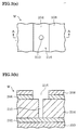
- An opening pattern 216 in a rough groove form having a larger opening area than the opening area of the via hole 210 and communicating with the opening of the via hole 210 is formed at the photoresist film 208 as illustrated in FIG. 2(a) and FIGS. 3(a) and 3(b) showing the state prior to the etching process.
- the reflection-preventing film 206 and the photoresist film 208 are removed concurrently in the embodiment.
- the embodiment may be adopted in conjunction with an organic film instead of the SiO 2 film 204.
- the wafer W shown in FIG. 2(a) is placed on the lower electrode 106 shown in FIG. 1.
- the processing gas e.g., a mixed gas containing O 2 and Ar
- the processing gas supply source 126 is induced into the processing chamber 102 from the processing gas supply source 126.
- vacuum drawing is implemented inside the processing chamber 102 to sustain the pressure at 10mTorr.
- plasma generating high-frequency power with its frequency set at 60 MHz and its level set at 1kW, for instance, is applied to the upper electrode 122.
- high-frequency power for biasing with its frequency set at 2 MHz and its power level set at a first level, i.e., 250 W, for instance, is applied to the lower electrode 106.
- the processing gas is raised to plasma by the plasma generating high-frequency power.
- ions in the plasma are induced into the wafer W by the high-frequency power for biasing.
- the photoresist film 208 becomes ashed, as illustrated in FIG. 2(b).
- the high-frequency power for biasing at the first power level which is relatively higher than a second power level to be detailed later and approximately equal to the power level set in the ashing method in the prior art described above, is also applied to the wafer W via the lower electrode 106.
- the fence portion 214 can be removed concurrently while grinding the photoresist film 208.
- the photoresist film 208 and the reflection-preventing film 206 are still not completely removed in the embodiment.
- the upper surface of the SiO 2 film 204 and shoulder portions 212a of the groove 212 are protected by the photoresist film 208 and the reflection-preventing film 206. Consequently, the upper surface of the SiO 2 film 204 and the shoulders portions 212a of the groove 212 are not exposed to the ions and, therefore, are not milled.
- the shape of the groove 212 and the thickness of the SiO 2 film 204 are not changed during the etching process.
- the high-frequency power for biasing applied to the lower electrode 106 is switched from the first power level to the second power level.
- the second power level is set relatively low compared to the first power level, e.g., 10 W or lower.
- the energy of the ions induced into the wafer W while applying highfrequency power for biasing at the second power level is reduced.
- the photoresist film 208 and the reflection-preventing film 206 can be removed without grinding the SiO 2 film 204 and the TiN film 202. It is to be noted that the other processing conditions are the same as those under which the high-frequency power for biasing at the first power level is applied.
- the high-frequency power for biasing is switched from the first power level to the second power level before the photoresist film 208 is completely removed as described above, and more desirably, before the photoresist film 208 is completely removed but after the fence portion 214 is removed, as illustrated in FIG. 2(b).
- the removal of the photoresist film 208 and the reflection-preventing film 206 and the removal of the fence portion 214 can be implemented in a single process, as illustrated in FIG. 2(c).
- a shoulders 210a of the via hole 210 and the shoulders 212a of the groove are not ground during this step.
- the timing with which the power level is switched is calculated in advance based upon the length of time required for the removal of the photoresist film 208 and the length of time required for the removal of the fence portion 214 and is set at the controller 120.
- the controller 120 controls the first high-frequency source 116 in conformance to the switching timing.
- the first high-frequency source 116 outputs the high-frequency power for biasing at the first power level to the lower electrode 106 during the period of time extending from the process start until the power level is switched.
- the first high-frequency source 116 outputs the high-frequency power for biasing at the second power level to the lower electrode 106 during the period of time extending from tire power level switch until the end of processing.
- This embodiment is characterized in that the supply of the high-frequency power for biasing at the first power level applied to the lower electrode 106 is stopped before the photoresist film 208 is completely removed. It is to be noted that since the apparatus in which the embodiment is adopted, the various conditions under which the process is implemented other than the condition with regard to the application of the high-frequency power for biasing to the lower electrode 106 and the structure of the wafer W undergoing the ashing process are identical to those in the first embodiment explained earlier, their explanation is omitted.
- the ashing process is first implemented on the wafer W shown in FIG. 2(a) placed on the lower electrode 106 by applying the high-frequency power for biasing at the first power level to the lower electrode 106 in FIG. 1 in the second embodiment.
- the photoresist film 208 is ashed and, at the same time, the fence portion 214 is removed as illustrated in FIG. 2(b).
- the controller 120 implements control on the first high-frequency source 116 to stop the output of the high-frequency power for biasing at the first power level before the photoresist film 208 is completely removed but after the fence portion 214 is removed, i.e., in the state illustrated in FIG. 2(b) and explained in reference to the first embodiment. Consequently, the energy of the ions induced to the wafer W is reduced to allow removal of the photoresist film 208 and the reflection-preventing film 206 without milling the SiO 2 film 204 and the TiN film 202, as shown in FIG. 2(c).
- a photoresist film 208 having a roughly circular opening pattern 300 is first formed over an SiO 2 film 204 at the wafer W.
- the opening pattern 300 is positioned so as to communicate with a first contact hole 302 and has a larger opening area then the opening area of the first contact hole 302.
- the SiO 2 film 204 is etched down to a specific depth of the first contact hole 302 at the wafer W to form a second contact hole having a larger internal diameter than the first contact hole 302 above the first contact hole 302.
- fence portion is formed around the opening of the first contact hole 302 at the bottom of the second contact hole.
- the present invention is not restricted by such details, and may be adopted in any of various other plasma processing apparatuses including a microwave plasma processing apparatus, an electron cyclotron resonance type plasma processing apparatus and an inductively coupled plasma processing apparatus.
- the fence portion formed during the etching process can be removed concurrently with the removal of the photoresist film, while maintaining the pattern achieved at the workpiece through the etching process.
Landscapes
- Physics & Mathematics (AREA)
- Engineering & Computer Science (AREA)
- Plasma & Fusion (AREA)
- General Physics & Mathematics (AREA)
- Drying Of Semiconductors (AREA)
- Exposure Of Semiconductors, Excluding Electron Or Ion Beam Exposure (AREA)
- Photosensitive Polymer And Photoresist Processing (AREA)
Abstract
Description
Claims (6)
- A plasma processing method for removing a photoresist film formed at a workpiece placed inside a processing chamber by raising a processing gas induced into said processing chamber to plasma, comprising:a step in which high-frequency power for biasing at a first power level is applied to the workpiece;a step in which the processing gas is raised to plasma; anda step in which high-frequency power for biasing at a second power level is applied to the workpiece by switching the high-frequency power for biasing at said first power level to the high-frequency power for biasing at said second power level lower than said first power level before said photoresist film is completely removed.
- A plasma processing method for removing a photoresist film formed at a workpiece placed inside a processing chamber by raising a processing gas induced into said processing chamber to plasma, comprising:a step in which high-frequency power for biasing is applied to the workpiece;a step in which the processing gas is raised to plasma; anda step in which application of the high-frequency power for biasing is stopped before said photoresist film is completely removed.
- A plasma processing method in which a photoresist film with an opening pattern having an opening area larger than the opening area of a hole formed at a specific layer of a workpiece and containing the opening of said hole is used as a mask to implement a plasma etching process halfway through said specific layer and then said photoresist film is removed, comprising:a step in which high-frequency power for biasing at a first power level is applied to the workpiece;a step in which the processing gas is raised to plasma; anda step in which high-frequency power for biasing at a second power level is applied to the workpiece by switching the high-frequency power for biasing at said first power level to the high-frequency power for biasing at said second power level lower than said first power level before the photoresist film is completely removed.
- A plasma processing method in which a photoresist film with an opening pattern having an opening area larger than the opening area of a hole formed at a specific layer of a workpiece and containing the opening of said hole is used as a mask to implement a plasma etching process halfway through said specific layer and then said photoresist film is removed, comprising:a step in which high-frequency power for biasing is applied to the workpiece;a step in which the processing gas is raised to plasma; anda step in which application of the high-frequency power for biasing is stopped before said photoresist film is completely removed.
- A plasma processing method according to any of claims 1 ∼ 4, wherein:said photoresist film constitutes a mask used to form a specific pattern at an SiO2 film formed at the workpiece.
- A plasma processing method according to any of claims 1 ∼ 4, wherein:said photoresist film constitutes a mask used to form a specific pattern at a film constituted of an organic material formed at the workpiece.
Applications Claiming Priority (2)
| Application Number | Priority Date | Filing Date | Title |
|---|---|---|---|
| JP27691299A JP4382926B2 (en) | 1999-09-29 | 1999-09-29 | Plasma processing method |
| JP27691299 | 1999-09-29 |
Publications (3)
| Publication Number | Publication Date |
|---|---|
| EP1091396A2 true EP1091396A2 (en) | 2001-04-11 |
| EP1091396A3 EP1091396A3 (en) | 2004-12-29 |
| EP1091396B1 EP1091396B1 (en) | 2012-07-25 |
Family
ID=17576130
Family Applications (1)
| Application Number | Title | Priority Date | Filing Date |
|---|---|---|---|
| EP00121014A Expired - Lifetime EP1091396B1 (en) | 1999-09-29 | 2000-09-27 | Plasma processing method |
Country Status (5)
| Country | Link |
|---|---|
| US (1) | US6743730B1 (en) |
| EP (1) | EP1091396B1 (en) |
| JP (1) | JP4382926B2 (en) |
| KR (1) | KR100603099B1 (en) |
| TW (1) | TW525212B (en) |
Families Citing this family (9)
| Publication number | Priority date | Publication date | Assignee | Title |
|---|---|---|---|---|
| JP2003017469A (en) * | 2001-06-29 | 2003-01-17 | Tokyo Electron Ltd | Etching / ashing apparatus, ashing apparatus, ashing method and processing method |
| US7700494B2 (en) * | 2004-12-30 | 2010-04-20 | Tokyo Electron Limited, Inc. | Low-pressure removal of photoresist and etch residue |
| US8202098B2 (en) * | 2005-02-28 | 2012-06-19 | Educational Testing Service | Method of model scaling for an automated essay scoring system |
| JP4827081B2 (en) * | 2005-12-28 | 2011-11-30 | 東京エレクトロン株式会社 | Plasma etching method and computer-readable storage medium |
| US7758763B2 (en) * | 2006-10-31 | 2010-07-20 | Applied Materials, Inc. | Plasma for resist removal and facet control of underlying features |
| US7768766B2 (en) | 2007-06-01 | 2010-08-03 | Lam Research Corporation | Plasma processing system ESC high voltage control |
| KR101500995B1 (en) * | 2008-11-06 | 2015-03-18 | 삼성전자 주식회사 | Plasma etching apparatus |
| CN103262221A (en) * | 2010-12-20 | 2013-08-21 | 株式会社爱发科 | Dielectric device manufacturing method and ashing method |
| CN106919010A (en) * | 2015-12-25 | 2017-07-04 | 中微半导体设备(上海)有限公司 | A device for stripping photoresist from a semiconductor wafer |
Family Cites Families (17)
| Publication number | Priority date | Publication date | Assignee | Title |
|---|---|---|---|---|
| JP3220992B2 (en) * | 1991-01-22 | 2001-10-22 | ソニー株式会社 | Dry etching method |
| US5250165A (en) * | 1991-12-09 | 1993-10-05 | Motorola, Inc. | Controlled isotropy reactive ion etcher for multi-stepped sloped contact etch process |
| KR0157536B1 (en) * | 1994-11-18 | 1998-12-01 | 모리시다 요이치 | Dry etching method |
| US5780359A (en) * | 1995-12-11 | 1998-07-14 | Applied Materials, Inc. | Polymer removal from top surfaces and sidewalls of a semiconductor wafer |
| US6043164A (en) * | 1996-06-10 | 2000-03-28 | Sharp Laboratories Of America, Inc. | Method for transferring a multi-level photoresist pattern |
| JP3122618B2 (en) * | 1996-08-23 | 2001-01-09 | 東京エレクトロン株式会社 | Plasma processing equipment |
| US5880018A (en) * | 1996-10-07 | 1999-03-09 | Motorola Inc. | Method for manufacturing a low dielectric constant inter-level integrated circuit structure |
| JP3251184B2 (en) * | 1996-11-01 | 2002-01-28 | 日本電気株式会社 | Resist removing method and resist removing apparatus |
| JP3316407B2 (en) * | 1997-02-26 | 2002-08-19 | シャープ株式会社 | Method for manufacturing semiconductor device |
| JP2897753B2 (en) | 1997-04-07 | 1999-05-31 | 株式会社日立製作所 | Sample post-treatment method |
| TW394989B (en) * | 1997-10-29 | 2000-06-21 | Matsushita Electronics Corp | Semiconductor device manufacturing and reaction room environment control method for dry etching device |
| JP3408409B2 (en) * | 1997-10-29 | 2003-05-19 | 松下電器産業株式会社 | Semiconductor device manufacturing method and reaction chamber environment control method for dry etching apparatus |
| JP3380846B2 (en) * | 1997-11-05 | 2003-02-24 | 松下電器産業株式会社 | Method for manufacturing semiconductor device |
| JP3218348B2 (en) * | 1998-05-21 | 2001-10-15 | 株式会社アルバック | Plasma ashing method |
| US6284149B1 (en) * | 1998-09-18 | 2001-09-04 | Applied Materials, Inc. | High-density plasma etching of carbon-based low-k materials in a integrated circuit |
| US6218084B1 (en) * | 1998-12-15 | 2001-04-17 | United Microelectronics Corp. | Method for removing photoresist layer |
| US6379574B1 (en) * | 1999-05-03 | 2002-04-30 | Applied Materials, Inc. | Integrated post-etch treatment for a dielectric etch process |
-
1999
- 1999-09-29 JP JP27691299A patent/JP4382926B2/en not_active Expired - Fee Related
-
2000
- 2000-09-20 TW TW089119378A patent/TW525212B/en not_active IP Right Cessation
- 2000-09-26 KR KR1020000056340A patent/KR100603099B1/en not_active Expired - Fee Related
- 2000-09-27 EP EP00121014A patent/EP1091396B1/en not_active Expired - Lifetime
- 2000-09-28 US US09/671,201 patent/US6743730B1/en not_active Expired - Lifetime
Also Published As
| Publication number | Publication date |
|---|---|
| KR100603099B1 (en) | 2006-07-20 |
| KR20010039919A (en) | 2001-05-15 |
| JP2001102361A (en) | 2001-04-13 |
| TW525212B (en) | 2003-03-21 |
| EP1091396B1 (en) | 2012-07-25 |
| EP1091396A3 (en) | 2004-12-29 |
| US6743730B1 (en) | 2004-06-01 |
| JP4382926B2 (en) | 2009-12-16 |
Similar Documents
| Publication | Publication Date | Title |
|---|---|---|
| KR100277843B1 (en) | Plasma processing system with reduced particle contamination | |
| US7749914B2 (en) | Plasma etching method | |
| US20060043066A1 (en) | Processes for pre-tapering silicon or silicon-germanium prior to etching shallow trenches | |
| US20020029853A1 (en) | Methods for running a high density plasma etcher to achieve reduced transistor device damage | |
| US20180005850A1 (en) | Selective etch using material modification and rf pulsing | |
| US6174370B1 (en) | Semiconductor wafer chucking device and method for stripping semiconductor wafer | |
| US6235640B1 (en) | Techniques for forming contact holes through to a silicon layer of a substrate | |
| KR101772701B1 (en) | Plasma etching method, plasma etching apparatus and computer-readable storage medium | |
| EP1143496A1 (en) | Plasma etching method | |
| US6406925B1 (en) | Method and apparatus for minimizing semiconductor wafer arcing during semiconductor wafer processing | |
| EP1091396A2 (en) | Plasma processing method | |
| KR100564082B1 (en) | Improved methods for performing planarization and recess etches and apparatus therefor | |
| JP3339597B2 (en) | Plasma processing method and plasma processing apparatus | |
| US7511936B2 (en) | Method and apparatus for dynamic plasma treatment of bipolar ESC system | |
| JP3350973B2 (en) | Plasma processing method and plasma processing apparatus | |
| JP3319083B2 (en) | Plasma processing method | |
| JPH1027780A (en) | Plasma treating method | |
| CN113192832A (en) | Substrate processing method and substrate processing system | |
| JP3247096B2 (en) | Plasma etching apparatus and plasma etching method | |
| JP7724281B2 (en) | Etching method and etching apparatus | |
| KR20040105356A (en) | Device for Removing Residual Electric Charge between Electrostatic Chuck and Wafer and Method the Same | |
| JP4373685B2 (en) | Plasma processing method | |
| KR20250146853A (en) | Method for treating a substrate and apparatus for treating a substrate | |
| KR100724195B1 (en) | Plasma Etching Device of Semiconductor Device | |
| JP2000077390A (en) | Plasma processing equipment |
Legal Events
| Date | Code | Title | Description |
|---|---|---|---|
| PUAI | Public reference made under article 153(3) epc to a published international application that has entered the european phase |
Free format text: ORIGINAL CODE: 0009012 |
|
| AK | Designated contracting states |
Kind code of ref document: A2 Designated state(s): AT BE CH CY DE DK ES FI FR GB GR IE IT LI LU MC NL PT SE |
|
| AX | Request for extension of the european patent |
Free format text: AL;LT;LV;MK;RO;SI |
|
| PUAL | Search report despatched |
Free format text: ORIGINAL CODE: 0009013 |
|
| AK | Designated contracting states |
Kind code of ref document: A3 Designated state(s): AT BE CH CY DE DK ES FI FR GB GR IE IT LI LU MC NL PT SE |
|
| AX | Request for extension of the european patent |
Extension state: AL LT LV MK RO SI |
|
| 17P | Request for examination filed |
Effective date: 20041124 |
|
| AKX | Designation fees paid |
Designated state(s): DE FR IT |
|
| GRAP | Despatch of communication of intention to grant a patent |
Free format text: ORIGINAL CODE: EPIDOSNIGR1 |
|
| GRAS | Grant fee paid |
Free format text: ORIGINAL CODE: EPIDOSNIGR3 |
|
| GRAA | (expected) grant |
Free format text: ORIGINAL CODE: 0009210 |
|
| AK | Designated contracting states |
Kind code of ref document: B1 Designated state(s): DE FR IT |
|
| REG | Reference to a national code |
Ref country code: DE Ref legal event code: R096 Ref document number: 60047373 Country of ref document: DE Effective date: 20120913 |
|
| PG25 | Lapsed in a contracting state [announced via postgrant information from national office to epo] |
Ref country code: IT Free format text: LAPSE BECAUSE OF FAILURE TO SUBMIT A TRANSLATION OF THE DESCRIPTION OR TO PAY THE FEE WITHIN THE PRESCRIBED TIME-LIMIT Effective date: 20120725 |
|
| PLBE | No opposition filed within time limit |
Free format text: ORIGINAL CODE: 0009261 |
|
| STAA | Information on the status of an ep patent application or granted ep patent |
Free format text: STATUS: NO OPPOSITION FILED WITHIN TIME LIMIT |
|
| REG | Reference to a national code |
Ref country code: FR Ref legal event code: ST Effective date: 20130531 |
|
| 26N | No opposition filed |
Effective date: 20130426 |
|
| REG | Reference to a national code |
Ref country code: DE Ref legal event code: R097 Ref document number: 60047373 Country of ref document: DE Effective date: 20130426 |
|
| PG25 | Lapsed in a contracting state [announced via postgrant information from national office to epo] |
Ref country code: FR Free format text: LAPSE BECAUSE OF NON-PAYMENT OF DUE FEES Effective date: 20121001 |
|
| PGFP | Annual fee paid to national office [announced via postgrant information from national office to epo] |
Ref country code: DE Payment date: 20170920 Year of fee payment: 18 |
|
| REG | Reference to a national code |
Ref country code: DE Ref legal event code: R119 Ref document number: 60047373 Country of ref document: DE |
|
| PG25 | Lapsed in a contracting state [announced via postgrant information from national office to epo] |
Ref country code: DE Free format text: LAPSE BECAUSE OF NON-PAYMENT OF DUE FEES Effective date: 20190402 |