EP1089603A2 - Copper foil bonding treatment with improved bond strength and resistance to undercutting - Google Patents
Copper foil bonding treatment with improved bond strength and resistance to undercutting Download PDFInfo
- Publication number
- EP1089603A2 EP1089603A2 EP00610100A EP00610100A EP1089603A2 EP 1089603 A2 EP1089603 A2 EP 1089603A2 EP 00610100 A EP00610100 A EP 00610100A EP 00610100 A EP00610100 A EP 00610100A EP 1089603 A2 EP1089603 A2 EP 1089603A2
- Authority
- EP
- European Patent Office
- Prior art keywords
- copper
- foil
- layer
- arsenic
- electrodeposited
- Prior art date
- Legal status (The legal status is an assumption and is not a legal conclusion. Google has not performed a legal analysis and makes no representation as to the accuracy of the status listed.)
- Withdrawn
Links
Images


Classifications
-
- H—ELECTRICITY
- H05—ELECTRIC TECHNIQUES NOT OTHERWISE PROVIDED FOR
- H05K—PRINTED CIRCUITS; CASINGS OR CONSTRUCTIONAL DETAILS OF ELECTRIC APPARATUS; MANUFACTURE OF ASSEMBLAGES OF ELECTRICAL COMPONENTS
- H05K3/00—Apparatus or processes for manufacturing printed circuits
- H05K3/38—Improvement of the adhesion between the insulating substrate and the metal
- H05K3/382—Improvement of the adhesion between the insulating substrate and the metal by special treatment of the metal
- H05K3/384—Improvement of the adhesion between the insulating substrate and the metal by special treatment of the metal by plating
-
- H—ELECTRICITY
- H05—ELECTRIC TECHNIQUES NOT OTHERWISE PROVIDED FOR
- H05K—PRINTED CIRCUITS; CASINGS OR CONSTRUCTIONAL DETAILS OF ELECTRIC APPARATUS; MANUFACTURE OF ASSEMBLAGES OF ELECTRICAL COMPONENTS
- H05K2201/00—Indexing scheme relating to printed circuits covered by H05K1/00
- H05K2201/03—Conductive materials
- H05K2201/0332—Structure of the conductor
- H05K2201/0335—Layered conductors or foils
- H05K2201/0355—Metal foils
-
- H—ELECTRICITY
- H05—ELECTRIC TECHNIQUES NOT OTHERWISE PROVIDED FOR
- H05K—PRINTED CIRCUITS; CASINGS OR CONSTRUCTIONAL DETAILS OF ELECTRIC APPARATUS; MANUFACTURE OF ASSEMBLAGES OF ELECTRICAL COMPONENTS
- H05K2203/00—Indexing scheme relating to apparatus or processes for manufacturing printed circuits covered by H05K3/00
- H05K2203/03—Metal processing
- H05K2203/0307—Providing micro- or nanometer scale roughness on a metal surface, e.g. by plating of nodules or dendrites
-
- H—ELECTRICITY
- H05—ELECTRIC TECHNIQUES NOT OTHERWISE PROVIDED FOR
- H05K—PRINTED CIRCUITS; CASINGS OR CONSTRUCTIONAL DETAILS OF ELECTRIC APPARATUS; MANUFACTURE OF ASSEMBLAGES OF ELECTRICAL COMPONENTS
- H05K2203/00—Indexing scheme relating to apparatus or processes for manufacturing printed circuits covered by H05K3/00
- H05K2203/07—Treatments involving liquids, e.g. plating, rinsing
- H05K2203/0703—Plating
- H05K2203/0723—Electroplating, e.g. finish plating
-
- Y—GENERAL TAGGING OF NEW TECHNOLOGICAL DEVELOPMENTS; GENERAL TAGGING OF CROSS-SECTIONAL TECHNOLOGIES SPANNING OVER SEVERAL SECTIONS OF THE IPC; TECHNICAL SUBJECTS COVERED BY FORMER USPC CROSS-REFERENCE ART COLLECTIONS [XRACs] AND DIGESTS
- Y10—TECHNICAL SUBJECTS COVERED BY FORMER USPC
- Y10T—TECHNICAL SUBJECTS COVERED BY FORMER US CLASSIFICATION
- Y10T428/00—Stock material or miscellaneous articles
- Y10T428/12—All metal or with adjacent metals
- Y10T428/12431—Foil or filament smaller than 6 mils
- Y10T428/12438—Composite
-
- Y—GENERAL TAGGING OF NEW TECHNOLOGICAL DEVELOPMENTS; GENERAL TAGGING OF CROSS-SECTIONAL TECHNOLOGIES SPANNING OVER SEVERAL SECTIONS OF THE IPC; TECHNICAL SUBJECTS COVERED BY FORMER USPC CROSS-REFERENCE ART COLLECTIONS [XRACs] AND DIGESTS
- Y10—TECHNICAL SUBJECTS COVERED BY FORMER USPC
- Y10T—TECHNICAL SUBJECTS COVERED BY FORMER US CLASSIFICATION
- Y10T428/00—Stock material or miscellaneous articles
- Y10T428/12—All metal or with adjacent metals
- Y10T428/12472—Microscopic interfacial wave or roughness
-
- Y—GENERAL TAGGING OF NEW TECHNOLOGICAL DEVELOPMENTS; GENERAL TAGGING OF CROSS-SECTIONAL TECHNOLOGIES SPANNING OVER SEVERAL SECTIONS OF THE IPC; TECHNICAL SUBJECTS COVERED BY FORMER USPC CROSS-REFERENCE ART COLLECTIONS [XRACs] AND DIGESTS
- Y10—TECHNICAL SUBJECTS COVERED BY FORMER USPC
- Y10T—TECHNICAL SUBJECTS COVERED BY FORMER US CLASSIFICATION
- Y10T428/00—Stock material or miscellaneous articles
- Y10T428/12—All metal or with adjacent metals
- Y10T428/12493—Composite; i.e., plural, adjacent, spatially distinct metal components [e.g., layers, joint, etc.]
- Y10T428/12535—Composite; i.e., plural, adjacent, spatially distinct metal components [e.g., layers, joint, etc.] with additional, spatially distinct nonmetal component
- Y10T428/12556—Organic component
- Y10T428/12569—Synthetic resin
-
- Y—GENERAL TAGGING OF NEW TECHNOLOGICAL DEVELOPMENTS; GENERAL TAGGING OF CROSS-SECTIONAL TECHNOLOGIES SPANNING OVER SEVERAL SECTIONS OF THE IPC; TECHNICAL SUBJECTS COVERED BY FORMER USPC CROSS-REFERENCE ART COLLECTIONS [XRACs] AND DIGESTS
- Y10—TECHNICAL SUBJECTS COVERED BY FORMER USPC
- Y10T—TECHNICAL SUBJECTS COVERED BY FORMER US CLASSIFICATION
- Y10T428/00—Stock material or miscellaneous articles
- Y10T428/12—All metal or with adjacent metals
- Y10T428/12493—Composite; i.e., plural, adjacent, spatially distinct metal components [e.g., layers, joint, etc.]
- Y10T428/12771—Transition metal-base component
- Y10T428/12785—Group IIB metal-base component
- Y10T428/12792—Zn-base component
-
- Y—GENERAL TAGGING OF NEW TECHNOLOGICAL DEVELOPMENTS; GENERAL TAGGING OF CROSS-SECTIONAL TECHNOLOGIES SPANNING OVER SEVERAL SECTIONS OF THE IPC; TECHNICAL SUBJECTS COVERED BY FORMER USPC CROSS-REFERENCE ART COLLECTIONS [XRACs] AND DIGESTS
- Y10—TECHNICAL SUBJECTS COVERED BY FORMER USPC
- Y10T—TECHNICAL SUBJECTS COVERED BY FORMER US CLASSIFICATION
- Y10T428/00—Stock material or miscellaneous articles
- Y10T428/12—All metal or with adjacent metals
- Y10T428/12493—Composite; i.e., plural, adjacent, spatially distinct metal components [e.g., layers, joint, etc.]
- Y10T428/12771—Transition metal-base component
- Y10T428/12861—Group VIII or IB metal-base component
- Y10T428/12903—Cu-base component
- Y10T428/1291—Next to Co-, Cu-, or Ni-base component
Definitions
- This invention relates to copper foil for use in manufacturing printed circuit boards, and, especially, to electrodeposited copper foil having a bonding side to be bonded to a polymeric substrate wherein the bonding side is provided with a copper bond-enhancing treatment layer, a copper-arsenic layer deposited on the bond-enhancing layer, and a zinc-containing layer deposited on the copper-arsenic layer.
- This invention also relates to copper clad laminates made with such foil, and to a process for producing such foil.
- a bonding treatment is effected by subjecting the bonding side, usually the matte side, of a "raw" electrodeposited copper foil to four consecutive electrodeposition steps.
- the first consists of the deposition of a microdendritic copper layer which enhances, to a very large degree, the real surface area of the matte side, and thus enhances the foil's bonding ability.
- electrodeposition of an encapsulating, or gilding, copper layer whose function is to reinforce mechanically the dendritic layer and thus render it immune to the lateral shear forces of liquid resins occurring in the laminating stage of printed circuit board (PCB) fabrication.
- the encapsulating step of the treatment is very important, since it eliminates the foil's tendency toward “treatment transfer” and the resulting "laminate staining" which can cause a decrease of the dielectric properties of copper-clad laminates.
- the shape, height, mechanical strength and the number of dendritic microprojections per unit of surface area which constitute the dendritic deposit are the factors instrumental in achieving adequate bond strength of the foil, after all stages of the treatment are completed, when the foil is bonded to a polymeric substrate.
- the role of the second treatment stage is to reinforce mechanically, the fragile dendritic layer, by overplating it with a thin layer of sound and strong metallic copper, which locks the dendrites to the base foil structure.
- Such a dendrites-encapsulation composite structure ought to be characterized by high bond strength and the absence of treatment transfer.
- the treating parameters which assure just that are relatively narrow. If the amount of the encapsulating, or gilding deposit is too low, the foil will be given to treatment transfer, and, if on the other hand, the gilding layer is too thick, a partial loss of peel strength may be expected.
- the layers are composed of pure copper, in the form of microscopic, spherical micro-projections.
- the electrodeposition of the copper bonding treatment is typically followed by deposition of a very thin layer of zinc or zinc alloy, a so-called barrier layer. Its purpose is to prevent direct copper-epoxy resin contact and that is why the zinc-alloy layer (which during lamination is converted to alpha brass), is called the barrier layer. If the bonding treatment composed of copper only is subjected to lamination with epoxy resin systems, it tends to react with amino groups of the resin, at the high laminating temperatures. It, in turn, creates moisture at the foil-resin interface, causing the harmful effect of "measling" and possibly delamination. A barrier layer which is plated over all-copper treatment prevents these harmful effects entirely. All three stages of the treatment mentioned above, effected by means of electrodeposition, change the geometry and morphology of the matte side of the foil, assuring the desired mechanical strength of the surface region, as well.
- the electrodeposition of the treatment is usually followed by an electrochemical stainproofing which changes the surface chemistry.
- the bonding surface is rendered chemically stable.
- This operation removes weak surface films, which can greatly decrease the adhesion of the solids, and replaces the films with a stable film of controlled thickness, which is responsible for imparting "durability" of its properties to the treated surface.
- the film serves as an undercoat for subsequent bonding.
- the same stainproofing step protects the opposite shiny side of the foil against atmospheric oxidation.
- These substrates which often are blends that involve multifunctional epoxies, BT resin, polyimide, etc., usually require an increased amount of bonding treatment to assure adequate peel-strength. It should be remembered that aside from its bond-enhancing microstructure, the amount of treatment per surface area of copper foil is also an important factor.
- foil manufacturers usually electrodeposit about 5 grams of dendritic deposit per square meter of copper foil and about the same amount of encapsulating deposit, while the mass of the barrier layer is usually about 1 gram per square meter.
- the amount of treatment deposited on the matte side of the foil depends on the current density and the plating time as determined by Faraday's Law. Current density cannot be increased excessively to accommodate higher treater speeds, since the copper foil has to carry the current between the contact rollers and the plating electrolyte.
- This zinc-alloy layer i.e., barrier layer
- barrier layer can be either plated "as is" or created by the heat accelerated diffusion of the metals.
- Some foil manufacturers electrodeposit a brass barrier layer.
- Others electrodeposit zinc.
- the foil delivered to the laminating plants has the bonding side characterized by a uniform gray color. Since the laminating process involves heat in the course of fabrication of copper clad laminates destined for PCBs, the zinc barrier layer alloys with the underlying all-copper bonding treatment by the process of heat-accelerated diffusion of metals in the solid state. As a result, a layer of yellow, chemically stable alpha brass is thus formed over the surface of all-copper surface.
- the Yates patent discloses the formation of the zinc alloy layer by either direct plating of brass, of the diffusion formation of brass.
- major foil manufacturers have introduced minor additional alloying elements to improve the performance of the barrier layer with respect to high temperatures of lamination required in the fabrication of polyimide laminates, high temperature post-bakes, etc.
- Metals like nickel, cobalt, tin, etc. may be co-deposited with zinc to achieve these goals.
- Red-ring undercut can be easily recognized when the conductor lines peeled back from the laminate surface exhibit pink outside margins quite different from the yellow color of un-attacked brass.
- Etching solutions can enter into the foil-epoxy interface, i.e., creep underneath conductor lines, leach out zinc from the brass layer and in effect diminish the functional width of the treated side of the foil that actually bonds track lines to the polymeric substrate.
- Red ring undercut is a textbook case of the corrosion of metal by mineral acids and etching solutions used in the fabrication of PCBs, through the process of "dezincification.” As the name implies, zinc is lost from the alloy, leaving as a residue, or by a process of redeposition, a porous mass of copper having little mechanical strength.
- Arsenic is a metal which, when added to brasses, e.g., those containing more than 15 wt % zinc, is most effective in preventing dezincification, and arsenic is added routinely (for the purpose of improving corrosion resistance) to metallurgical brasses, i.e., those produced by melting of metals.
- a primary object of the present invention is a treated copper foil which, when bonded to a polymeric substrate, has an improved bond strength to the substrate and provides good resistance to undercutting by acids used in etching to form electrical circuitry on copper-clad laminates made with the foil.
- Another object of the invention is a copper-clad laminate made with the above foil which enables a durable, high strength bond between the foil and its substrate.
- Still a further object of the invention is a process for electrodepositing a treatment on a bonding side of an electrolytic copper foil, which treatment provides an improved bond strength and resistance to undercutting.
- a treated copper foil for use in the manufacture of printed circuit boards which comprises an electrodeposited copper base foil having a bonding side upon which there is deposited a bonding treatment which includes a copper bond-enhancing treatment layer electrodeposited on the bonding side; a copper-arsenic layer electrodeposited on the bond-enhancing treatment layer; and a barrier layer of zinc or a zinc alloy electrodeposited on the copper-arsenic layer.
- the above treated copper foil may be produced by a process for electrodepositing a treatment on a bonding side of a copper base foil, which process comprises electrodepositing a bond-enhancing copper treatment layer on a bonding side of the base foil; co-electrodepositing copper and arsenic on the bond-enhancing treatment from an electrolyte containing copper ions and arsenic ions under electrodeposition conditions effective to deposit thereon a copper-arsenic alloy layer; and electrodepositing zinc or a zinc alloy on the copper-arsenic layer to deposit thereon a zinc or zinc alloy barrier layer.
- an electrodeposited copper base foil 10 is produced on a rotating drum-cathode by a well-known process, and it has a shiny side 12, or drum side, and matte side 14 (the side facing the electrolyte) with a velvety finish formed of, on a micro-scale, peaks and valleys.
- a bond-enhancing copper treatment layer 16 is electrodeposited on a bonding side of the foil (the side to be bonded to a polymeric substrate when forming a copper-clad laminate for the manufacture of PCBs), which may be either the matte side or the shiny side, but preferably is the matte side.
- Treatment 16 preferably is formed of a plurality of electrodeposited layers, e.g., a copper dendritic layer followed by a gilding (or encapsulating) copper layer.
- the purpose of treatment 16 is to enhance the bond strength of the foil to a polymeric substrate when a copper-clad laminate is formed.
- the copper bond-enhancing treatment 16 can be deposited by any suitable technique, for example, the technique disclosed in U.S. Patent No. 3,857,681 (Yates et al.), which is incorporated herein by reference.
- a microcrystalline copper-arsenic layer 18 is electrodeposited on the treatment layer 16, as described herein below.
- a zinc or zinc alloy barrier layer 20 is then electrodeposited on microcrystalline layer 18, using a well-known method, preferably the method disclosed in the above-mentioned U.S. Patent No 3,857,681.
- arsenic is introduced into a barrier layer (initially composed of zinc or zinc alloy), by:
- This "bonding" (lamination) operation is accomplished in laminating plants and involves heating and cooling cycles. Sheets of copper foil are laid on sheets of "prepreg” (e.g., glass fabric impregnated with epoxy resin). Both materials are placed in a hydraulic press with heated pressing plates and pressed together under high pressure. At elevated temperatures, the resin liquefies and is forced, by pressure, into micro-irregularities of the foil surface. This is followed by a second cycle where both materials are cooled while pressure is maintained. The resin solidifies in the irregularities of the foil surface to firmly bond both materials together, making them very difficult to pull apart.
- the laminating temperatures depend on the type of the polymeric substrate but are in general of the order of 350 - 450°F. The heat is applied for several hours.
- microcrystalline layer has been found to also provide a significant improvement in peel-strength (bond-strength) of copper foil when it is bonded to a polymeric substrate.
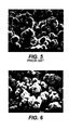
- the basic shape of an individual treatment particle 16 is a sphere whose average diameter is about 2 microns (when treatment is applied as per prior art: U.S. Patent 3,857,681, 4,572,768, or 5,207,889).
- the spheres formed by combination of dendritic and encapsulating layers are in addition covered by needles (or whiskers), of the microcrystalline layer 18.
- needles or whiskers
- These needles are an average 0.2 microns in diameter and 0.6 microns in height. This, in addition enlarges the true surface area available for bonding and increases the roughness factor of the bonding treatment (the ratio of the true surface area to the apparent or projected area). Thus, a higher bond strength is achieved.
- a web of 1 ounce (35 microns thick) electrodeposited raw copper foil was processed through a treater machine, in order to provide the matte side of the raw foil with a bonding treatment.
- Foils No. 1 and No. 2 were tested for peel-strength (bond strength) and resistance to undercutting, after being laminated to FR-4 epoxy polymeric substrate (prepreg of glass fiber and epoxy resin, designated FR-4 by the National Electrical Manufacturers Association-NEMA).
- Bond strength was measured as follows: The foil was bonded to an epoxy resin-impregnated fiberglass support in a conventional manner. The epoxy resin was used in its "B" stage and was cured in contact with the treated surface of the foil under a pressure of about 500 psi at about 330°-340°F. The final thickness of the laminate over approximately 1/16th of an inch with the foil comprising about 0.0015 inches of this total. The laminate so constructed was then cut into 1 ⁇ 2 inch wide strips and subjected to bond strength tests in the following manner: Copper was peeled from the glass cloth support at a rate of 2 inches per minute in a direction perpendicular to the laminate. The force required to peel the copper from the support was read on a force gauge and was measured in pounds of force. This reading was doubled to obtain the peel strength per inch of width of laminate. A bond strength of 10 lbs./in. of width of laminate is deemed to be very acceptable. A bond strength of 12 lbs./in. or more is deemed to be exceptional.
- the main features of the electrolyte and the process for the deposition of microcrystalline layer are:
- Co-deposition of arsenic is achieved by introduction into the electrolyte of arsenic in the form of ortho-arsenic acid H 3 AsO 4 , of rather low concentration.
- H 3 AsO 4 ortho-arsenic acid
- a mere 2% of As in the microcrystalline deposit is enough to effect immunity to undercutting; however, it may be found desirable to use other amounts, for example, from about 0.5 to 5 wt % As.
Landscapes
- Engineering & Computer Science (AREA)
- Manufacturing & Machinery (AREA)
- Microelectronics & Electronic Packaging (AREA)
- Laminated Bodies (AREA)
- Manufacturing Of Printed Wiring (AREA)
- Electroplating Methods And Accessories (AREA)
- Parts Printed On Printed Circuit Boards (AREA)
- Electroplating And Plating Baths Therefor (AREA)
Abstract
Description
| PARAMETERS OF THE PROCESS AND THE ELECTROLYTE FOR ELECTRODEPOSITION OF COPPER/ARSENIC MICROCRYSTALLINE LAYER | ||
| PARAMETER | MOST PREFERRED | PREFERRED RANGE |
| Cu as CuSO4 | 5 g/l | 4 - 8 g/l |
| As as H3AsO4 | 250 ppm | 200 - 300 ppm |
| H2SO4 | 40 g/l | 35 - 45 g/l |
| Chloride | 8 ppm | 5 - 20 ppm |
| Temperature | Ambient | 15 - 30°C |
| Current Density | 6 A/dm2 | 4 - 8 A/dm2 |
| Time | 5 sec. | 3-8 sec. |
| Cu in the Deposit | 0.59 g/m2 | 0.3 g/m2 - 1.0 g/m2 |
| As in the Deposit | 0.013 g/m2 | 0.005 g/m2 - 0.05 g/m2 |
| Undercutting | ||||
| Bond Strength lbs/inch | Bond Strength lbs/mm | Bond Strength after HCI Ibs/mm | Bond Strength loss % | |
| Foil No. 1 | 10.6 | 0.41 | 0.35 | 13 |
| Foil No. 2 | 12.2 | 0.48 | 0.48 | 0 |
- very low copper concentration
- low temperature
- high current density
- absence of vigorous agitation
- presence of chloride ions
Claims (13)
- A treated copper foil for use in the manufacture of printed circuit boards, which comprises:(a) an electrodeposited copper base foil having a bonding side upon which there is deposited a bonding treatment which includes:(b) a copper bond-enhancing treatment layer electrodeposited on the bonding side;(c) a copper-arsenic layer electrodeposited on the bond-enhancing treatment layer; and(d) a barrier layer of zinc or a zinc alloy electrodeposited on the copper-arsenic layer.
- The copper foil of claim 1, wherein the copper-arsenic layer is composed of, by weight, from about 95% to about 99.5% copper and from about 0.5% to about 5% arsenic.
- The copper foil of claim 2, wherein the copper-arsenic layer is a copper-arsenic alloy composed of, by weight, about 98% copper and about 2% arsenic.
- A copper clad laminate comprising a polymeric substrate and the copper foil of claim 1, wherein the substrate is bonded through the bonding treatment to the bonding side of the copper foil.
- The laminate of claim 4, wherein at least a portion of the barrier layer is a copper-zinc-arsenic alloy formed by solid-solid diffusion.
- The copper foil of claim 1, wherein the copper base foil has a shiny side and a matte side, and the bond-enhancing treatment layer is electrodeposited on the matte side of the base foil.
- The copper foil of claim 1, wherein the copper base foil has a shiny side and a matte side, and the bond-enhancing treatment layer is electrodeposited on the shiny side of the base foil.
- The copper foil of claim 1, wherein the bond-enhancing treatment layer includes a dendritic copper layer deposited on the bonding side of the foil and an encapsulating copper layer deposited on the dendritic layer.
- The copper foil of claim 1, wherein the bond-enhancing treatment layer is a plurality of electrodeposited copper layers.
- A process for electrodepositing a treatment on a bonding side of a copper base foil, which process comprises:(a) electrodepositing a bond-enhancing copper treatment layer on a bonding side of the base foil;(b) co-electrodepositing copper and arsenic on the bond-enhancing treatment from an electrolyte containing copper ions and arsenic ions under electrodeposition conditions effective to deposit thereon a copper-arsenic alloy layer; and(c) electrodepositing zinc or a zinc alloy on the copper-arsenic layer to deposit thereon a zinc or zinc alloy barrier layer.
- The process of claim 10, wherein the electrolyte comprises an aqueous-sulfuric acid solution containing copper ions, arsenic ions and chloride ions.
- The process of claim 10, wherein the electrodeposition conditions include the use of an electrolyte which is an aqueous solution containing, per liter of the solution, from about 4-8 grams per liter of copper; from about 200 to about 300 parts per million of arsenic; from about 35 to about 45 grams per liter of H2SO4; and from about 5 to about 20 parts per million of chloride ions; and wherein there is employed a current density of from about 4 to about 8 amperes per square decimeter, and a plating time of from about 3 to about 8 seconds.
- The process of claim 10, wherein the copper base foil is an electrodeposited copper foil having a shiny side and a matte side, and the bond-enhancing copper layer is electrodeposited on the matte side.
Applications Claiming Priority (2)
| Application Number | Priority Date | Filing Date | Title |
|---|---|---|---|
| US408170 | 1989-09-15 | ||
| US09/408,170 US6342308B1 (en) | 1999-09-29 | 1999-09-29 | Copper foil bonding treatment with improved bond strength and resistance to undercutting |
Publications (2)
| Publication Number | Publication Date |
|---|---|
| EP1089603A2 true EP1089603A2 (en) | 2001-04-04 |
| EP1089603A3 EP1089603A3 (en) | 2002-04-17 |
Family
ID=23615139
Family Applications (1)
| Application Number | Title | Priority Date | Filing Date |
|---|---|---|---|
| EP00610100A Withdrawn EP1089603A3 (en) | 1999-09-29 | 2000-09-28 | Copper foil bonding treatment with improved bond strength and resistance to undercutting |
Country Status (4)
| Country | Link |
|---|---|
| US (1) | US6342308B1 (en) |
| EP (1) | EP1089603A3 (en) |
| JP (1) | JP2001177205A (en) |
| CN (1) | CN1301130A (en) |
Cited By (1)
| Publication number | Priority date | Publication date | Assignee | Title |
|---|---|---|---|---|
| CN105874891A (en) * | 2013-12-30 | 2016-08-17 | 日进材料股份有限公司 | Copper foil, and electrical component and battery including same |
Families Citing this family (8)
| Publication number | Priority date | Publication date | Assignee | Title |
|---|---|---|---|---|
| US20020182432A1 (en) * | 2000-04-05 | 2002-12-05 | Masaru Sakamoto | Laser hole drilling copper foil |
| KR100442564B1 (en) * | 2001-10-23 | 2004-07-30 | 엘지전선 주식회사 | Electrodeposited copper foil for PCB with barrier layer of Zn-Co-As alloy and surface treatment of the copper foil |
| KR100480154B1 (en) | 2002-08-30 | 2005-04-06 | 엘지.필립스 엘시디 주식회사 | Touch Panel |
| TWI263461B (en) * | 2003-12-26 | 2006-10-01 | Ind Tech Res Inst | Enhanced flexible copper foil structure and fabrication method thereof |
| US20170016131A1 (en) * | 2015-07-15 | 2017-01-19 | Far East University | Growth method of dendritic crystal structure that provides directional heat transfer |
| JP6789965B2 (en) * | 2015-11-05 | 2020-11-25 | 古河電気工業株式会社 | Lead frame material and its manufacturing method |
| KR102413300B1 (en) * | 2020-12-10 | 2022-06-27 | 와이엠티 주식회사 | Metal foil, carrier with metal foil comprising the same and printed circuit board comprising the same |
| CN115791387B (en) * | 2022-10-14 | 2026-04-17 | 沪士电子股份有限公司 | A test method for the bonding strength between fiberglass cloth and resin |
Family Cites Families (14)
| Publication number | Priority date | Publication date | Assignee | Title |
|---|---|---|---|---|
| US3857681A (en) | 1971-08-03 | 1974-12-31 | Yates Industries | Copper foil treatment and products produced therefrom |
| BE789715A (en) * | 1971-10-08 | 1973-02-01 | Yates Industries | MULTI-LAYER COPPER SHEET TREATMENT |
| JPS5515216A (en) * | 1978-07-20 | 1980-02-02 | Mitsui Anakonda Dohaku Kk | Printed circut copper foil and method of manufacturing same |
| WO1982002991A1 (en) * | 1981-02-26 | 1982-09-02 | Torday John | Treatment of copper foil |
| DE3371096D1 (en) * | 1982-12-01 | 1987-05-27 | Electrofoils Techn Ltd | Treatment of copper foil |
| US4572768A (en) | 1985-06-28 | 1986-02-25 | Square D Company | Treatment for copper foil |
| US5207886A (en) | 1988-02-16 | 1993-05-04 | Applied Biosystems, Inc. | Capillary electrophoresis |
| US4915797A (en) * | 1989-05-24 | 1990-04-10 | Yates Industries, Inc. | Continuous process for coating printed circuit grade copper foil with a protective resin |
| KR930006103B1 (en) * | 1991-03-11 | 1993-07-07 | 덕산금속 주식회사 | Printed circuit for electrolysis copper foil & method |
| KR930001934B1 (en) * | 1991-03-11 | 1993-03-20 | 덕산금속 주식회사 | Electrolysis copper foil & making method for printed circuit |
| US5332486A (en) * | 1993-01-29 | 1994-07-26 | Gould Electronics Inc. | Anti-oxidant coatings for copper foils |
| US5482784A (en) * | 1993-12-24 | 1996-01-09 | Mitsui Mining And Smelting Co., Ltd. | Printed circuit inner-layer copper foil and process for producing the same |
| US5679230A (en) * | 1995-08-21 | 1997-10-21 | Oak-Mitsui, Inc. | Copper foil for printed circuit boards |
| US6060666A (en) * | 1997-12-22 | 2000-05-09 | Foil Technology Development Corporation | Electrolytic layer applied to metallic foil to promote adhesion to a polymeric substrate |
-
1999
- 1999-09-29 US US09/408,170 patent/US6342308B1/en not_active Expired - Fee Related
-
2000
- 2000-09-28 EP EP00610100A patent/EP1089603A3/en not_active Withdrawn
- 2000-09-29 CN CN00128414.2A patent/CN1301130A/en active Pending
- 2000-09-29 JP JP2000300752A patent/JP2001177205A/en active Pending
Cited By (1)
| Publication number | Priority date | Publication date | Assignee | Title |
|---|---|---|---|---|
| CN105874891A (en) * | 2013-12-30 | 2016-08-17 | 日进材料股份有限公司 | Copper foil, and electrical component and battery including same |
Also Published As
| Publication number | Publication date |
|---|---|
| CN1301130A (en) | 2001-06-27 |
| JP2001177205A (en) | 2001-06-29 |
| US6342308B1 (en) | 2002-01-29 |
| EP1089603A3 (en) | 2002-04-17 |
Similar Documents
| Publication | Publication Date | Title |
|---|---|---|
| US8674229B2 (en) | Ultra-thin copper foil with carrier and copper-clad laminate board or printed circuit board substrate | |
| EP0072830B1 (en) | Treatment of copper foil | |
| CA1277948C (en) | Treatment for copper foil | |
| JP2002292788A (en) | Composite copper foil and method for manufacturing the same | |
| JP3295308B2 (en) | Electrolytic copper foil | |
| TWI645755B (en) | Surface-treated copper foil, copper foil with carrier, substrate, resin substrate, printed wiring board, copper-clad laminate, and printed wiring board manufacturing method | |
| CN101892499A (en) | Peelable ultra-thin copper foil with copper foil as carrier and preparation method thereof | |
| US5447619A (en) | Copper foil for the manufacture of printed circuit boards and method of producing the same | |
| KR100595381B1 (en) | Composite copper foil, manufacturing method thereof and copper clad laminate and printed wiring board using the composite copper foil | |
| US5989727A (en) | Electrolytic copper foil having a modified shiny side | |
| US6372113B2 (en) | Copper foil and copper clad laminates for fabrication of multi-layer printed circuit boards and process for producing same | |
| US6342308B1 (en) | Copper foil bonding treatment with improved bond strength and resistance to undercutting | |
| US6610418B1 (en) | Electolytic copper foil with carrier foil and method for manufacturing the same | |
| JP4612978B2 (en) | Composite copper foil and method for producing the same | |
| EP0250195A2 (en) | Double matte finish copper foil | |
| KR20210143727A (en) | Metal foil for printed wiring board, metal foil provided with carrier, and metal clad laminated board, and manufacturing method of a printed wiring board using them | |
| KR100684812B1 (en) | Novel composite foil, manufacturing method thereof, and copper clad laminate | |
| EP0520640A1 (en) | Metal foil with improved peel strength and method for making said foil | |
| EP0839440B1 (en) | Copper foil for the manufacture of printed circuits and method of producing same | |
| EP0996318B1 (en) | Novel composite foil, process for producing the same and copper-clad laminate | |
| CA2070046A1 (en) | Metal foil with improved bonding to substrates and method for making said foil | |
| US6042711A (en) | Metal foil with improved peel strength and method for making said foil | |
| JP5854872B2 (en) | Copper foil with carrier, method for producing copper foil with carrier, laminate and method for producing printed wiring board | |
| JP3615973B2 (en) | Novel composite foil and manufacturing method thereof, copper-clad laminate | |
| CN114990656A (en) | Copper foil for manufacturing multilayer complex PCB, preparation method and additive for preparation |
Legal Events
| Date | Code | Title | Description |
|---|---|---|---|
| PUAI | Public reference made under article 153(3) epc to a published international application that has entered the european phase |
Free format text: ORIGINAL CODE: 0009012 |
|
| AK | Designated contracting states |
Kind code of ref document: A2 Designated state(s): AT BE CH CY DE DK ES FI FR GB GR IE IT LI LU MC NL PT SE Kind code of ref document: A2 Designated state(s): DE FR GB IT LU SE |
|
| AX | Request for extension of the european patent |
Free format text: AL;LT;LV;MK;RO;SI |
|
| PUAL | Search report despatched |
Free format text: ORIGINAL CODE: 0009013 |
|
| AK | Designated contracting states |
Kind code of ref document: A3 Designated state(s): AT BE CH CY DE DK ES FI FR GB GR IE IT LI LU MC NL PT SE |
|
| AX | Request for extension of the european patent |
Free format text: AL;LT;LV;MK;RO;SI |
|
| AKX | Designation fees paid |
Free format text: DE FR GB IT LU SE |
|
| STAA | Information on the status of an ep patent application or granted ep patent |
Free format text: STATUS: THE APPLICATION IS DEEMED TO BE WITHDRAWN |
|
| 18D | Application deemed to be withdrawn |
Effective date: 20021018 |