EP1089095A2 - Process and device for producing photonic crystal, and optical element - Google Patents
Process and device for producing photonic crystal, and optical element Download PDFInfo
- Publication number
- EP1089095A2 EP1089095A2 EP00308306A EP00308306A EP1089095A2 EP 1089095 A2 EP1089095 A2 EP 1089095A2 EP 00308306 A EP00308306 A EP 00308306A EP 00308306 A EP00308306 A EP 00308306A EP 1089095 A2 EP1089095 A2 EP 1089095A2
- Authority
- EP
- European Patent Office
- Prior art keywords
- light
- optical
- refractive index
- optical medium
- wavelength
- Prior art date
- Legal status (The legal status is an assumption and is not a legal conclusion. Google has not performed a legal analysis and makes no representation as to the accuracy of the status listed.)
- Granted
Links
- 230000003287 optical effect Effects 0.000 title claims abstract description 482
- 239000004038 photonic crystal Substances 0.000 title claims abstract description 151
- 238000000034 method Methods 0.000 title claims abstract description 78
- 230000008569 process Effects 0.000 title claims abstract description 75
- 238000009826 distribution Methods 0.000 claims abstract description 53
- 239000013078 crystal Substances 0.000 claims abstract description 41
- 238000011282 treatment Methods 0.000 claims abstract description 11
- 239000000178 monomer Substances 0.000 claims description 20
- 239000000126 substance Substances 0.000 claims description 11
- 238000010438 heat treatment Methods 0.000 claims description 5
- 230000005855 radiation Effects 0.000 claims description 5
- 239000011148 porous material Substances 0.000 claims description 4
- 230000001902 propagating effect Effects 0.000 claims 8
- 230000008859 change Effects 0.000 abstract description 68
- VYPSYNLAJGMNEJ-UHFFFAOYSA-N Silicium dioxide Chemical compound O=[Si]=O VYPSYNLAJGMNEJ-UHFFFAOYSA-N 0.000 description 203
- 239000000377 silicon dioxide Substances 0.000 description 98
- 230000000737 periodic effect Effects 0.000 description 63
- 239000003822 epoxy resin Substances 0.000 description 45
- 229920000647 polyepoxide Polymers 0.000 description 45
- 239000013598 vector Substances 0.000 description 32
- 230000001788 irregular Effects 0.000 description 20
- 238000004519 manufacturing process Methods 0.000 description 19
- CSCPPACGZOOCGX-UHFFFAOYSA-N Acetone Chemical compound CC(C)=O CSCPPACGZOOCGX-UHFFFAOYSA-N 0.000 description 18
- OKKJLVBELUTLKV-UHFFFAOYSA-N Methanol Chemical compound OC OKKJLVBELUTLKV-UHFFFAOYSA-N 0.000 description 18
- 238000010521 absorption reaction Methods 0.000 description 17
- 239000012327 Ruthenium complex Substances 0.000 description 15
- 229920000642 polymer Polymers 0.000 description 15
- 229920005989 resin Polymers 0.000 description 15
- 239000011347 resin Substances 0.000 description 15
- 229920003229 poly(methyl methacrylate) Polymers 0.000 description 13
- 230000005684 electric field Effects 0.000 description 12
- LNEPOXFFQSENCJ-UHFFFAOYSA-N haloperidol Chemical compound C1CC(O)(C=2C=CC(Cl)=CC=2)CCN1CCCC(=O)C1=CC=C(F)C=C1 LNEPOXFFQSENCJ-UHFFFAOYSA-N 0.000 description 11
- 239000000463 material Substances 0.000 description 11
- LFQSCWFLJHTTHZ-UHFFFAOYSA-N Ethanol Chemical compound CCO LFQSCWFLJHTTHZ-UHFFFAOYSA-N 0.000 description 10
- 239000010432 diamond Substances 0.000 description 10
- 229910003460 diamond Inorganic materials 0.000 description 10
- 238000000059 patterning Methods 0.000 description 10
- 239000004926 polymethyl methacrylate Substances 0.000 description 10
- 230000008901 benefit Effects 0.000 description 9
- 230000007246 mechanism Effects 0.000 description 9
- 230000015572 biosynthetic process Effects 0.000 description 8
- 230000014509 gene expression Effects 0.000 description 8
- 230000001678 irradiating effect Effects 0.000 description 8
- 239000000758 substrate Substances 0.000 description 8
- VVQNEPGJFQJSBK-UHFFFAOYSA-N Methyl methacrylate Chemical compound COC(=O)C(C)=C VVQNEPGJFQJSBK-UHFFFAOYSA-N 0.000 description 7
- 230000000694 effects Effects 0.000 description 7
- 230000001747 exhibiting effect Effects 0.000 description 6
- 238000006116 polymerization reaction Methods 0.000 description 6
- 239000002253 acid Substances 0.000 description 5
- 239000010419 fine particle Substances 0.000 description 5
- 239000004065 semiconductor Substances 0.000 description 5
- 229910052814 silicon oxide Inorganic materials 0.000 description 5
- XKRFYHLGVUSROY-UHFFFAOYSA-N Argon Chemical compound [Ar] XKRFYHLGVUSROY-UHFFFAOYSA-N 0.000 description 4
- 239000000470 constituent Substances 0.000 description 4
- 239000010408 film Substances 0.000 description 4
- 239000003999 initiator Substances 0.000 description 4
- 239000013307 optical fiber Substances 0.000 description 4
- 229920000058 polyacrylate Polymers 0.000 description 4
- 230000004044 response Effects 0.000 description 4
- 230000003595 spectral effect Effects 0.000 description 4
- 238000001228 spectrum Methods 0.000 description 4
- 238000000411 transmission spectrum Methods 0.000 description 4
- RTAQQCXQSZGOHL-UHFFFAOYSA-N Titanium Chemical compound [Ti] RTAQQCXQSZGOHL-UHFFFAOYSA-N 0.000 description 3
- -1 acryl Chemical group 0.000 description 3
- 229910052786 argon Inorganic materials 0.000 description 3
- 239000000835 fiber Substances 0.000 description 3
- 238000010030 laminating Methods 0.000 description 3
- 238000005459 micromachining Methods 0.000 description 3
- 230000000750 progressive effect Effects 0.000 description 3
- 239000010936 titanium Substances 0.000 description 3
- 229910052719 titanium Inorganic materials 0.000 description 3
- 238000005452 bending Methods 0.000 description 2
- 230000005540 biological transmission Effects 0.000 description 2
- 229910052792 caesium Inorganic materials 0.000 description 2
- TVFDJXOCXUVLDH-UHFFFAOYSA-N caesium atom Chemical compound [Cs] TVFDJXOCXUVLDH-UHFFFAOYSA-N 0.000 description 2
- 238000005530 etching Methods 0.000 description 2
- 239000011159 matrix material Substances 0.000 description 2
- 229910052751 metal Inorganic materials 0.000 description 2
- 239000002184 metal Substances 0.000 description 2
- 230000005012 migration Effects 0.000 description 2
- 238000013508 migration Methods 0.000 description 2
- 230000010287 polarization Effects 0.000 description 2
- 239000002243 precursor Substances 0.000 description 2
- 150000003303 ruthenium Chemical class 0.000 description 2
- 239000010409 thin film Substances 0.000 description 2
- 239000011800 void material Substances 0.000 description 2
- NIXOWILDQLNWCW-UHFFFAOYSA-M Acrylate Chemical compound [O-]C(=O)C=C NIXOWILDQLNWCW-UHFFFAOYSA-M 0.000 description 1
- 230000005374 Kerr effect Effects 0.000 description 1
- 230000005697 Pockels effect Effects 0.000 description 1
- 230000005699 Stark effect Effects 0.000 description 1
- ZHAFUINZIZIXFC-UHFFFAOYSA-N [9-(dimethylamino)-10-methylbenzo[a]phenoxazin-5-ylidene]azanium;chloride Chemical compound [Cl-].O1C2=CC(=[NH2+])C3=CC=CC=C3C2=NC2=C1C=C(N(C)C)C(C)=C2 ZHAFUINZIZIXFC-UHFFFAOYSA-N 0.000 description 1
- 238000002679 ablation Methods 0.000 description 1
- 230000009471 action Effects 0.000 description 1
- 239000011230 binding agent Substances 0.000 description 1
- 239000003054 catalyst Substances 0.000 description 1
- 230000003197 catalytic effect Effects 0.000 description 1
- 238000006243 chemical reaction Methods 0.000 description 1
- 150000001875 compounds Chemical class 0.000 description 1
- 229920001577 copolymer Polymers 0.000 description 1
- RKTYLMNFRDHKIL-UHFFFAOYSA-N copper;5,10,15,20-tetraphenylporphyrin-22,24-diide Chemical compound [Cu+2].C1=CC(C(=C2C=CC([N-]2)=C(C=2C=CC=CC=2)C=2C=CC(N=2)=C(C=2C=CC=CC=2)C2=CC=C3[N-]2)C=2C=CC=CC=2)=NC1=C3C1=CC=CC=C1 RKTYLMNFRDHKIL-UHFFFAOYSA-N 0.000 description 1
- JBPCDMSEJVCNGV-UHFFFAOYSA-N coumarin 334 Chemical compound C1CCC2=C(OC(C(C(=O)C)=C3)=O)C3=CC3=C2N1CCC3 JBPCDMSEJVCNGV-UHFFFAOYSA-N 0.000 description 1
- 238000000354 decomposition reaction Methods 0.000 description 1
- 230000008034 disappearance Effects 0.000 description 1
- 238000010894 electron beam technology Methods 0.000 description 1
- 238000011156 evaluation Methods 0.000 description 1
- 238000001704 evaporation Methods 0.000 description 1
- 230000008020 evaporation Effects 0.000 description 1
- 230000005284 excitation Effects 0.000 description 1
- 230000004927 fusion Effects 0.000 description 1
- 239000007789 gas Substances 0.000 description 1
- PCHJSUWPFVWCPO-UHFFFAOYSA-N gold Chemical compound [Au] PCHJSUWPFVWCPO-UHFFFAOYSA-N 0.000 description 1
- 239000010931 gold Substances 0.000 description 1
- 229910052737 gold Inorganic materials 0.000 description 1
- 238000009434 installation Methods 0.000 description 1
- 230000010354 integration Effects 0.000 description 1
- 238000006317 isomerization reaction Methods 0.000 description 1
- 239000007788 liquid Substances 0.000 description 1
- 238000001459 lithography Methods 0.000 description 1
- 239000000203 mixture Substances 0.000 description 1
- 230000004048 modification Effects 0.000 description 1
- 238000012986 modification Methods 0.000 description 1
- 239000011022 opal Substances 0.000 description 1
- 239000002245 particle Substances 0.000 description 1
- 238000006552 photochemical reaction Methods 0.000 description 1
- 238000007699 photoisomerization reaction Methods 0.000 description 1
- 230000000379 polymerizing effect Effects 0.000 description 1
- SCUZVMOVTVSBLE-UHFFFAOYSA-N prop-2-enenitrile;styrene Chemical compound C=CC#N.C=CC1=CC=CC=C1 SCUZVMOVTVSBLE-UHFFFAOYSA-N 0.000 description 1
- 239000010453 quartz Substances 0.000 description 1
- 238000002310 reflectometry Methods 0.000 description 1
- 238000010992 reflux Methods 0.000 description 1
- 238000003980 solgel method Methods 0.000 description 1
- 239000002904 solvent Substances 0.000 description 1
- 238000004544 sputter deposition Methods 0.000 description 1
- 229920000638 styrene acrylonitrile Polymers 0.000 description 1
- WGPCGCOKHWGKJJ-UHFFFAOYSA-N sulfanylidenezinc Chemical group [Zn]=S WGPCGCOKHWGKJJ-UHFFFAOYSA-N 0.000 description 1
- 238000005406 washing Methods 0.000 description 1
Images








Classifications
-
- G—PHYSICS
- G02—OPTICS
- G02B—OPTICAL ELEMENTS, SYSTEMS OR APPARATUS
- G02B6/00—Light guides; Structural details of arrangements comprising light guides and other optical elements, e.g. couplings
- G02B6/10—Light guides; Structural details of arrangements comprising light guides and other optical elements, e.g. couplings of the optical waveguide type
- G02B6/12—Light guides; Structural details of arrangements comprising light guides and other optical elements, e.g. couplings of the optical waveguide type of the integrated circuit kind
- G02B6/122—Basic optical elements, e.g. light-guiding paths
- G02B6/1225—Basic optical elements, e.g. light-guiding paths comprising photonic band-gap structures or photonic lattices
-
- G—PHYSICS
- G02—OPTICS
- G02F—OPTICAL DEVICES OR ARRANGEMENTS FOR THE CONTROL OF LIGHT BY MODIFICATION OF THE OPTICAL PROPERTIES OF THE MEDIA OF THE ELEMENTS INVOLVED THEREIN; NON-LINEAR OPTICS; FREQUENCY-CHANGING OF LIGHT; OPTICAL LOGIC ELEMENTS; OPTICAL ANALOGUE/DIGITAL CONVERTERS
- G02F1/00—Devices or arrangements for the control of the intensity, colour, phase, polarisation or direction of light arriving from an independent light source, e.g. switching, gating or modulating; Non-linear optics
- G02F1/01—Devices or arrangements for the control of the intensity, colour, phase, polarisation or direction of light arriving from an independent light source, e.g. switching, gating or modulating; Non-linear optics for the control of the intensity, phase, polarisation or colour
- G02F1/03—Devices or arrangements for the control of the intensity, colour, phase, polarisation or direction of light arriving from an independent light source, e.g. switching, gating or modulating; Non-linear optics for the control of the intensity, phase, polarisation or colour based on ceramics or electro-optical crystals, e.g. exhibiting Pockels effect or Kerr effect
-
- B—PERFORMING OPERATIONS; TRANSPORTING
- B82—NANOTECHNOLOGY
- B82Y—SPECIFIC USES OR APPLICATIONS OF NANOSTRUCTURES; MEASUREMENT OR ANALYSIS OF NANOSTRUCTURES; MANUFACTURE OR TREATMENT OF NANOSTRUCTURES
- B82Y20/00—Nanooptics, e.g. quantum optics or photonic crystals
Definitions
- This invention relates to a process and a device for producing an optical element having a photonic-band structure, particularly an optical element comprising a three-dimensional photonic crystal having a desired crystal structure easily and in a short period of time, and it also relates to an optical element produced by using the process and the device.
- the present invention relates to an optical element and an optical demultiplexer. More specifically, it relates to an active optical element and an optical demultiplexer that have achieved an optical switching function by changing a photonic-band structure by switching external fields such as light and an electric field in a photonic crystal.
- This phenomenon is similar to the phenomenon that electron energy in a semiconductor shows a band structure in a periodic potential.
- the photonic crystal is significantly characterized by its optical properties since it is capable of making the so-called "photonic-bandgap" in which light does not transmit in any directions (E. Yablonovitch, Phys. Rev. Lett. 58(20), 2059(1987)) appear and has very high degrees of optical anisotropy and dispersibility.
- optical properties since it is capable of making the so-called "photonic-bandgap" in which light does not transmit in any directions (E. Yablonovitch, Phys. Rev. Lett. 58(20), 2059(1987)) appear and has very high degrees of optical anisotropy and dispersibility.
- the conventional process taking advantage of the self-arrangement of silicon oxide fine particles has problems associated with reliability and reproducibility. Meanwhile, since other processes require that each layer be laminated with high accuracy to form the periods of a photonic crystal, even if they succeed in the formation of the photonic crystal, it takes long time, the number of repeating periods is limited, and a desired crystal structure cannot be formed freely.
- the photonic crystal has been conventionally used as a "passive element", and they have been rarely proposed to be used as an "active element".
- most of the conventionally proposed photonic crystals are determined their optical properties by the refractive-index distribution fixed in space. Therefore, in an optical demultiplexer, for example, the wavelength (frequency) of light to be transmitted in a specific direction is fixed, and the frequency of light to be derived in a specific direction has not been able to be switched. It has also not been possible to dynamically switch the direction of light from one direction of a branch placed in a waveguide to the other direction thereof.
- the above proposal (4) merely switches between the appearance and the disappearance of the function as the photonic crystal, and does not change actively the manner in which the function as the photonic crystal appears. Therefore, it cannot be used for controlling the direction in an optical demultiplexer or the branching in an optical waveguide.
- the above proposal (5) due to its structure, can only apply to a one-dimensional photonic crystal, and cannot apply to a two-dimensional or three-dimensional photonic crystal having high dispersibility and excellent properties as waveguides.
- the above proposal (6) changes the band structure by changing the complex refractive indices of the optical media constituting the photonic crystal, and cannot change the periodicity and symmetry of the photonic crystal. Therefore, it cannot induce a change in a large band structure.
- the conventional photonic crystals even when imparted with an active function, have been limited to the action of selecting whether the function itself as the photonic crystal should appear or disappear, in the number of dimensions of the photonic crystal capable of switching and to a particular controllable range.
- the prior arts use a process of changing only the refractive indices of optical materials of different types without changing distributions thereof, cannot switch the crystal structure and periodicity of the photonic crystal, and cannot change the structure of a photonic-band freely and dynamically.
- the production process of the optical element of the present invention is a process for producing an optical element comprising a photonic crystal in which spots having different refractive indices are arranged periodically, which comprises the step of placing an optical medium, whose refractive index changes by irradiation of light or by conducting predetermined treatment after the irradiation of light according to the intensity of the applied light, in a field where light intensity changes at a period of the wavelength order of light in space and keeping the medium therein for a given time; and the step of repeating at least once the step of changing the position of the optical medium and having the above field acted on the medium again.
- optical medium used in the present invention there can be used one whose refractive index changes, according to the intensity of applied light, by setting the medium aside for a given time after irradiation of light, or by subjecting the medium to heat treatment, irradiation of electromagnetic wave or corpuscular radiation, or treatment with chemicals after the irradiation of light.
- the optical field where light intensity changes at a period of the wavelength order of light in space is created, for example, by interference of a laser beam.
- a piezo element-incorporated stage that can shift the optical medium in three directions of x, y and z is used, for example.
- the production device of the optical element of the present invention comprises an optical system that creates an optical field where light intensity changes in space at a period of the wavelength order of light, and a movable stage that keeps an optical medium whose refractive index changes according to the intensity of applied light in the optical field where light intensity changes periodically and that can shift the optical medium for a minute distance of the wavelength order of light in the field.
- the production device of the optical element of the present invention may further comprise a light source and a detector for evaluating the optical element produced.
- the optical element of the present invention that is produced by the above process and the above device is an optical element comprising a photonic crystal in which spots having different refractive indices are arranged periodically, wherein a spot with a certain refractive index which constitutes the photonic crystal is located at a lattice point of a desired crystal structure; the refractive index distribution of an optical medium located at each lattice point has a shape having projections or bulges in the directions of three different axes; the crystal structure is not a simple lattice or the shape of the refractive index distribution of an optical medium located at each lattice point is not isotropic; and the refractive index distributions of optical media located at the lattice points together forming a simple lattice have the same shape and direction.
- the optical element of the present invention has a structure comprising the first optical medium in which the second optical medium and the third optical medium are periodically arranged at an interval of the wavelength order of incident light.
- the relative relationship among the refractive indices of the first to third, that is, the first, the second and the third optical media is changed by changing the external field condition applied to the above structure, whereby the periodicity of the spacial distribution of the refractive indices formed in the above structure can be changed.
- wavelength order of light indicates an interval of about the same order as the wavelength of light.
- the interval is not significantly different from the wavelength of light, as exemplified by at least several tens of times or at most several tenths of the wavelength.
- the optical element of the present invention has a one-dimensional, two-dimensional or three-dimensional structure in which at least three types of optical media are arranged periodically.
- Optical materials, temperature and external field conditions are selected so that the refractive indices of at least two optical media should be different from each other to the frequency of incident light.
- the light having a given wavelength is modulated by the periodic arrangement of the second optical medium, whereas since the refractive index of the first optical medium and that of the second optical medium are substantially the same and the refractive index of the first optical medium and that of the third optical medium are substantially different to the light having a given wavelength under the second external field condition different from the first external field condition, the light having a given wavelength is modulated by the periodic arrangement of the third optical medium.
- the structure having a periodic structure is constituted by three types of optical media, which are each defined as the first optical medium, the second optical medium and the third optical medium and whose refractive indices are each defined as the first refractive index, the second refractive index and the third refractive index, the distribution of each of the first, the second and the third optical media in the structure has a periodic structure.
- the periodic structure of the refractive index by which incident light is modulated in the structure is determined mainly by the periodic distribution of the second medium.
- the refractive index of the first medium and that of the second medium become about the same and the refractive index of the first medium and that of the third medium become different in the above wavelength, that is, the difference between the first refractive index and the third refractive index becomes larger than the difference between the first refractive index and the second refractive index, whereby the periodic structure of the refractive index by which incident light is modulated in the structure is determined mainly by the periodic distribution of the third medium instead, so that a new band structure appears in the wavelength range associated with incident light.
- the third optical element of the present invention has a structure comprising the first optical medium, the second optical medium arranged periodically in the first optical medium, and the third optical medium which has been substituted for and arranged in continuous spots of the periodic structure that should be formed by the second optical medium in the first optical medium.
- the continuous spots substituted by the third optical medium function as a waveguide to the light having a given wavelength
- the complex refractive index of the second optical medium and the complex refractive index of the third optical medium are substantially the same to the light having a given wavelength under the second external field condition different from the first external field condition
- the continuous spots substituted by the third optical medium do not function as a waveguide to the light having a given wavelength.
- the above third optical element has a two-dimensional or three-dimensional structure which comprises at least two types of optical media having different complex refractive indices and in which spots formed of the same type of optical medium are arranged periodically.
- the irregularities in the periodic structure of this structure exist as one-dimensionally continuous spots in the structure, and the one-dimensionally continuous spots function as an optical waveguide.
- three optical media out of these optical media are each defined as the first optical medium, the second optical medium and the third optical medium, and the complex refractive indices of the first, the second and the third optical media in the vicinity of the frequency ⁇ of light to be inputted in this waveguide are each defined as the first complex refractive index, the second complex refractive index and the third complex refractive index, this structure has a two-dimensional or three-dimensional periodic structure formed of the second optical medium in the first optical medium, a portion of the two-dimensional or three-dimensional periodic structure formed of the second optical medium is substituted by the one-dimensionally continuous spots formed of the third medium, the first complex refractive index and the second complex refractive index are different and the second complex refractive index and the third complex refractive index are also different in the vicinity of the frequency of light inputted in this optical element, and the spots substituted by the third medium function as an optical waveguide.
- this optical element is imparted with a waveguide having a switching function.
- the fourth optical element of the present invention has a structure comprising the first optical medium, the second optical medium arranged periodically in the first optical medium, the third optical medium which has been substituted for and arranged in the first continuous portion of the periodic structure that should be formed by the second optical medium in the first optical medium, the fourth optical medium which has been substituted for and arranged in the second continuous portion of the periodic structure that should be formed by the second optical medium in the first optical medium, and the third continuous portion of the periodic structure which should be formed by the second optical medium and in which the periodicity of the second medium is irregular; and the first portion and the second portion are connected to the third portion.
- the fourth optical element since, under the first external field condition, the complex refractive index of the first optical medium, the complex refractive index of the second optical medium and the complex refractive index of the third optical medium are different from one another to light having a given wavelength, and the complex refractive index of the second optical medium and the complex refractive index of the fourth optical medium are substantially the same to the light having a given wavelength, the first portion and the third portion function as waveguides to the light having a given wavelength.
- the fourth optical element of the present invention is capable of switching the heading direction of the light having a given wavelength which has been inputted in the third portion either to the first portion or to the second portion.
- the above fourth optical element has a two-dimensional or three-dimensional structure which comprises at least two types of optical media having different complex refractive indices and in which spots formed of the same type of optical medium are arranged periodically.
- the irregularities in the periodic structure of this structure exist as one-dimensionally continuous spots in the structure, and the one-dimensionally continuous spots function as an optical waveguide.
- these optical media are each defined as the first optical medium, the second optical medium, the third optical medium and the fourth optical medium, and the complex refractive indices of the first to the fourth optical media in the vicinity of the frequency of light to be inputted in this optical waveguide are each defined as the first complex refractive index, the second complex refractive index, the third complex refractive index and the fourth complex refractive index, this structure has a two-dimensional or three-dimensional periodic structure formed of the second optical medium in the first optical medium, a portion of the two-dimensional or three-dimensional periodic structure formed of the second optical medium is substituted by the one-dimensionally continuous portion formed of the third medium to form the first portion, another portion thereof is substituted by the one-dimensionally continuous portion formed of the fourth medium to form the second portion, one-dimensionally continuous irregularities in the periodic structure of the second medium are formed in still another portion thereof to form the third portion, and the first portion and the second portion are connected to the third portion.
- the first complex refractive index and the second complex refractive index are different, the second complex refractive index and the third complex refractive index are also different, and the second complex refractive index and the fourth complex refractive index are about the same in the vicinity of the frequency of light to be inputted in this optical element, the third portion and the first portion function as optical waveguides for the incident light.
- the second complex refractive index and the fourth complex refractive index become different and the second complex refractive index and the third complex refractive index become about the same while the first complex refractive index and the second complex refractive index remain different in the vicinity of the frequency ⁇ , whereby the first portion no longer functions as the irregularity in the periodic structure to the incident light and therefore no longer functions as an optical waveguide while the second portion starts to function as an optical waveguide instead.
- the above fourth optical element is capable of switching the heading direction of the light inputted in the third portion between the first portion and the second portion.
- the optical demultiplexer of the present invention has a structure comprising the first optical medium, the second optical medium arranged periodically in the first optical medium, the third optical medium which has been substituted for and arranged in the first continuous portion of the periodic structure that should be formed by the second optical medium in the first optical medium, the fourth optical medium which has been substituted for and arranged in the second continuous portion of the periodic structure that should be formed by the second optical medium in the first optical medium, and the third continuous portion of the periodic structure which should be formed by the second optical medium and in which the periodicity of the second medium is irregular; and the first portion and the second portion are connected to the third portion.
- the complex refractive index of the first optical medium, the complex refractive index of the second optical medium and the complex refractive index of the third optical medium are different from one another to light having the first wavelength, and the complex refractive index of the second optical medium and the complex refractive index of the fourth optical medium are substantially the same to the light having the first wavelength, the first portion and the third portion function as waveguides to the light having the first wavelength.
- this optical demultiplexer is capable of directing the light having the first wavelength or the second wavelength which has been inputted in the third portion either to the first portion or to the second portion depending on wavelength thereof.
- the optical demultiplexer of the present invention has a two-dimensional or three-dimensional structure which comprises at least two types of optical media having different complex refractive indices and in which spots formed of the same type of optical medium are arranged periodically.
- the irregularities in the periodic structure of this structure exist as one-dimensionally continuous spots in the structure, and the one-dimensionally continuous spots function as a waveguide.
- this structure has a two-dimensional or three-dimensional periodic structure formed of the second optical medium in the first optical medium, a portion of the two-dimensional or three-dimensional periodic structure formed of the second optical medium is substituted by the one-dimensionally continuous portion formed of the third medium to form the first portion, another portion thereof is substituted by
- the first complex refractive index and the second complex refractive index are different, the second complex refractive index and the third complex refractive index are also different, and the second complex refractive index and the fourth complex refractive index are about the same in the vicinity of the first frequency of light to be inputted in this optical element, the third portion and the first portion function as optical waveguides for the incident light, whereas since the fifth complex refractive index and the sixth complex refractive index are different, the sixth complex refractive index and the eighth complex refractive index are also different, and the sixth complex refractive index and the seventh complex refractive index are about the same in the vicinity of the second frequency, the third portion and the second portion function as optical waveguides for the incident light.
- the light having the first wavelength or the second wavelength which ha been inputted in the third portion heads either to the first portion or to the second portion depending on wavelength thereof, enabling the waveguide itself to function as an optical demultiplexer.
- the response of the photonic crystal to incident light is determined by the spacial distribution of refractive index in the frequency (wavelength) of controlled light, i.e., incident light (or a certain range of frequencies when the incident light is not monochromatic light) in functioning as an optical element and is not influenced by the distribution of refractive index in other wavelength range.
- the active optical element according to the present invention uses a plurality of optical media whose refractive indices change by an external field.
- the refractive indices of two optical media out of the plurality of optical media are caused to be the same or about the same under a certain external field condition.
- the periodic distribution of refractive index that light senses is the distribution pattern of optical media other than the two optical media having the same refractive index.
- the refractive indices of two other optical media are caused to be the same under other external field condition.
- light in the optical element senses the distribution pattern of optical media other than the optical media having the same refractive index under the external field condition.
- two significantly different photonic-band structures can be switched from one to the other by switching between the external field conditions.
- the switchable waveguide in the photonic crystal according to the present invention operates by switching between the portions where the periodicity of refractive index is irregular in the crystal structure.
- the optical demultiplexer relies not on the switching of external field conditions, but on the frequency (wavelength) of incident light to cause changes in the refractive indices of optical media.
- the photonic crystal and the waveguide are constituted by a combination of optical media that can form a photonic crystal in which the portions that light senses as the irregularities in the periodicity of refractive index vary according to the frequency of the light, and caused to function as the optical demultiplexer.
- the photonic crystal can be produced by repeating the step of forming every spot where the refractive index changes that corresponds to the same site in each unit cell at a time for the number of sites in a unit cell by shifting the optical medium as much as a minute distance by taking advantage of the translational symmetry of the crystal, they are easy to operate, and a three-dimensional photonic crystal with multiple periods in the wavelength range of light that has been virtually almost impossible to produce with the prior art can be produced in the form of a desired crystal structure with high accuracy by the production process and the production device of the present invention.
- a combination of optical media having the largest refractive index difference change in the frequency of controlled light to be inputted, or new spots having different refractive indices from the existing spots appear periodically, that is, a new periodic structure is formed after the change, or the ratio of the periodic peaks of the refractive indices of the media which occur in the periodic structure changes, where the response of the photonic crystal or the waveguide can be actively switched.
- spots that become a portion of the periodic structure of refractive index depending on the wavelength of the controlled light at other locations there can be produced an optical demultiplexer in which light heads to different waveguides at a branch according to the wavelength thereof.
- Fig. 1 is a perspective view showing a spot having high light intensity which has been formed on a lattice point constituting a three-dimensional rectangular-system structure in accordance with the process of the present invention.
- Fig. 2 is a perspective view showing the device used in example 1 of the present invention for producing an optical element.
- Fig. 3 is a perspective view showing the structure of the photonic crystal produced in example 1 of the present invention.
- Fig. 4 is a conceptual illustration exemplifying the case where the distribution of refractive index has a form having bulges in the directions of three different axes.
- Fig. 5 shows the chemical formula of the photopolymerization initiator used in example 2.
- Fig. 6 is a perspective view showing the device used in example 4 of the present invention for producing an optical element.
- Fig. 7 shows the transmission spectrum of the photonic crystal produced in example 4 of the present invention.
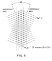
- Fig. 8 shows a process for forming a one-dimensional periodic structure of light intensity by the interference of two progressive waves heading in different directions in accordance with the present invention.
- Fig. 9 is a conceptual illustration showing the distribution of refractive index in the photonic crystal.
- Fig. 10 is a conceptual illustration showing the distribution of refractive index in the photonic crystal.
- Fig. 11 is a conceptual illustration showing the distribution of refractive index in the photonic crystal.
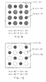
- Fig. 12 shows the switching from a cesium chloride-type structure to a body-centered cubic structure by switching external field conditions.
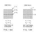
- Fig. 13 shows the switching in an optical waveguide.
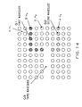
- Fig. 14 shows the distribution of refractive index in an optical waveguide which is capable of switching the direction of incident light according to an external field condition.
- Fig. 15 shows the states of switching the transmitting directions of light in an optical waveguide according to external field conditions.
- Fig. 16 is a conceptual illustration showing the distribution of refractive index in an optical demultiplexer according to the optical waveguide in the photonic crystal.
- Fig. 17 is a conceptual illustration showing the dependencies of the refractive indices of optical media on external field conditions.
- Fig. 18 shows the chemical structure of a ruthenium complex used in an example of the present invention as a catalyst for photopolymerization reaction.
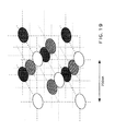
- Fig. 19 shows the distribution of the ruthenium complex in porous silica at some point in the process of producing an example of the photonic crystal of the present invention. To be seen clearly, each layer is shadowed differently, starting from the most front layer.
- Fig. 20 shows the structure of an example of the photonic crystal of the present invention. Only the first layer is shown.
- Fig. 21 shows the reflection spectrum of the photonic crystal of Fig. 20.
- Fig. 22 shows the arrangement of dye-containing epoxy resins at some point in the process of producing an example of the optical waveguide in the photonic crystal of the present invention.
- Fig. 23 shows the switching behavior in an example of the optical waveguide in the photonic crystal of the present invention.
- Fig. 24 shows the connection of waveguides in an example of the optical waveguide in the photonic crystal of the present invention.
- an optical medium whose refractive index changes according to the intensity of applied light by irradiation of light only, by setting the optical medium aside for a given time after the irradiation of light, or by subjecting it to heat treatment, irradiation of electromagnetic wave (such as light) or corpuscular radiation (such as electron beam, ⁇ -beam or neutron beam), or treatment with chemicals after the irradiation of light. It is preferable that the change in the refractive index of the optical medium be induced by the above predetermined treatments after irradiation of light rather than by the irradiation of light only.
- the optical medium showing such a change in refractive index can also be expressed as follows. That is, when the ratio between the maximum refractive index value and the minimum refractive index value in the optical medium before irradiation of light is defined as r(1), the ratio between the maximum refractive index value and the minimum refractive index value in the optical medium after the irradiation of light is defined as r(2), and the ratio between the maximum refractive index value and the minimum refractive index value in the optical medium after the completion of the treatment for causing a change in refractive index is defined as r(3), the optical medium that can be suitably used in the present invention preferably satisfies such conditions that
- a mechanism to cause a change in the refractive index of the material used in the above optical medium there can be used a mechanism to cause a change in the refractive index by the chemical change undergoing the photopolymerization process of a polymerizable monomer or the polymerization process thereof comprising a combination of a photochemical reaction and temperature elevation, a mechanism to cause a change in the refractive index by population migration caused by irradiating a hole burning substance with light, or a mechanism to cause a change in the refractive index by irradiating a photoisomerizable compound with light.
- a mechanism to cause a change in the refractive index by decomposing or modifying molecules in the light-irradiated portions of the optical medium by local temperature elevation or intense light there can also be used.
- a photopolymerizable monomer is impregnated into an inorganic porous material having high porosity to cause photopolymerization, only the monomer is then washed out and removed to form voids, and a change in the refractive index may be caused to appear by the residual polymer and the air present in the voids of the porous material.
- a material having a high refractive index is filled in the voids of the porous material from which the monomer has been removed, and a change in the refractive index may be caused to appear by the residual polymer and the filled material. In this case, there may not be a change in refractive index between the monomer before the irradiation of light and the polymer produced by the irradiation of light.
- an optical field where light intensity changes periodically in space is provided.
- Such an optical field can be created by using a stationary wave generated by interference between a laser beam heading in a certain direction and a laser beam heading in the opposite direction by reflecting the laser beam by a mirror, or by using an interference pattern in between progressive waves heading in at least two directions.
- the process of the present invention has paid attention to the fact that the lattice points of a three-dimensional cubic lattice have translational symmetry and is characterized by repeating the above "baking" more than once by shifting the position of the optical medium as much as a minute distance which is about the same as the wavelength of light for each "baking".
- each spot corresponding to a certain site in a unit cell constituting a desired crystal structure to be formed throughout the optical medium can be "baked” at a time. Then, the position of the optical medium is slightly shifted to match the position where light intensity is high in the optical medium to another site in the unit cell constituting the desired crystal structure, and "baking” is conducted again. The step of shifting the optical medium and conducting “baking” is repeated until every spot corresponding to every site in the unit cell constituting the crystal structure is "baked".
- the desired photonic crystal structure is obtained by allowing changes in the refractive indices of the "baked” spots to complete by setting the optical medium aside for a given time, or by causing the changes in the refractive indices of the "baked” spots to appear by predetermined treatments such as irradiation of light.
- site indicates the position corresponding to the position of each atom in the unit cell.
- the step of forming every spot where the refractive index changes that corresponds to the atom at the same site in each unit cell at a time is repeated for "the number of sites in a unit cell". Therefore, it is not necessary to repeat the step for "the number of periods or atoms" that constitute the crystal, as in conventional processes.
- it is easy to move one "baking" site to another "baking" site since it can be accomplished just by slightly shifting the three-dimensional optical medium.
- the same photonic crystal can also be produced by driving the whole optical system for creating the optical field where light intensity changes periodically.
- the photonic crystal can be produced more easily and more accurately by the process of the present invention than by driving the whole optical system because, in the process of the present invention, the optical medium is shifted.
- the production device for the optical element of the present invention comprises an optical system that creates an optical field where light intensity changes in space at a period of the wavelength order of light, and a movable stage that keeps an optical medium whose refractive index changes according to the intensity of applied light in the optical field where light intensity changes periodically and that can shift the optical medium for a minute distance of the wavelength order of light in the optical field.
- the phrase "wavelength order of light” as used herein indicates a wavelength of about 100 nm to 10 ⁇ m in the range from ultraviolet light to infrared light.
- the optical system that creates the optical field where light intensity changes at a period of the wavelength order of light in space will be explained by taking the case where the interference of a laser beam is employed as an example.
- laser beams having frequencies of ⁇ x , ⁇ y and ⁇ z are irradiated toward the origin point along with the x, y and z axes, respectively.
- a mirror for reflecting the laser beam is placed, via the origin point, a mirror for reflecting the laser beam, perpendicularly to the axis.
- incoming beam and reflected beam thereof interfere with each other to form a standing wave having a period of C a /(2 ⁇ x ), C a /(2 ⁇ y ) or C a /(2 ⁇ z ) in space.
- C a is the light velocity in a medium (such as air).
- Light intensity is high at loops of these standing waves, and the point where the loops of the three one-dimensional standing waves having periodicity in the respective direction are overlapped with one another is said to be a point having particularly high light intensity.
- the values of ⁇ x , ⁇ y and ⁇ z are selected according to the size of a unit cell of a photonic crystal to be formed.
- the incoming directions of the three laser beams and the orientations of the mirrors for reflecting the beams are determined according to the crystal structure of a photonic crystal to be formed, and they are not necessarily perpendicular to each other.
- the optical medium is desirably one on which "baking” occurs by the chemical change or the formation of a polymer precursor by multi-photon absorption such as two-photon absorption, or one on which "baking" occurs by the light intensity of a certain threshold.
- the spacial modulation of refractive index is defined. As described above, it is desirable that there be a time lag between the exposure for "baking” and the actual occurrence of a change in refractive index. Further, as described above, it is desirable that a change in refractive index do not appear until the predetermined treatment such as heating or irradiation of light is carried out after the formation of a latent image by "baking".
- the "baking" process itself occur not only by the effect of an optical field where light intensity periodically changes, but in combination with other factors such as gate beam. This is because if "baking" does not occur when a laser beam that incurs interference is irradiated on an optical medium, the position of the optical medium can be adjusted while the laser beam that generates an interference pattern is actually irradiated on the optical medium. It is desirable that "baking" be conducted by, for example, the irradiation of a gate beam after the position of the optical medium is set.
- the device of the present invention is equipped with a movable stage that keeps an optical medium in an optical field where light intensity periodically changes and can shift the optical medium for a minute distance of the wavelength order of light in the field.
- the optical medium is shifted for a minute distance in the spacially fixed field of periodic light intensity to conduct "baking" on each site in a unit cell.
- the minute distance ranges from about the wavelength of light to about one/tenth thereof (to 100 nm).
- the optical medium can be shifted with great accuracy by the piezo element-driven stage.
- the crystal structure of a photonic crystal to be formed is determined.
- the formation of the crystal structure can be controlled by varying the intensity of applied light and the time of irradiation, or by conducting "baking" on a particular site twice or three times by shifting the optical medium slightly.
- the production device for the optical element of the present invention further comprises a light source and a detector for evaluating an optical element formed so as to check the formation of a photonic-bandgap, it becomes possible to produce the optical element while the performance of the photonic crystal is checked.
- an optical medium is placed at the origin point (0, 0, 0) to conduct the first "baking".
- an optical medium is placed at the origin point (0, 0, 0) to conduct the first "baking”.
- the optical medium is shifted for a vector of (a/2, 0, a/2) from the origin point to conduct the second "baking".
- the optical medium is then shifted for a vector of (0, a/2, a/2) from the origin point to conduct the third "baking".
- a laser beam is irradiated toward the origin point along with each of the x, y and z axes that are orthogonal to one another with the relationship among the frequencies of the three laser beams being ⁇ 1 ⁇ ⁇ 2 , ⁇ 2 ⁇ ⁇ 3 and ⁇ 1 ⁇ ⁇ 3 , and standing waves are formed by the interference between the three laser beams and reflected beams thereof from mirrors placed, via the origin point, at the other sides of the axes.
- an optical medium is placed at the origin point (0, 0, 0) to conduct the first "baking".
- a laser beam is irradiated toward the origin point along with each of the x, y and z axes that are orthogonal to one another with the relationship among the frequencies of the three laser beams being ⁇ 1 ⁇ ⁇ 2 , ⁇ 2 ⁇ ⁇ 3 and ⁇ 1 ⁇ ⁇ 3 , and standing waves are formed by the interference between the three laser beams and reflected beams thereof from mirrors placed, via the origin point, at the other sides of the axes.
- an optical medium is placed at the origin point (0, 0, 0) to conduct the first "baking".
- the optical medium is shifted for a vector of (a/2, 0, c/2) from the origin point to conduct the second "baking".
- the optical medium is then shifted for a vector of (0, b/2, c/2) from the origin point to conduct the third "baking”.
- a laser beam is irradiated toward the origin point along with each of the x, y and z axes that are orthogonal to one another with the relationship among the frequencies of the three laser beams being ⁇ 1 ⁇ ⁇ 2 , ⁇ 2 ⁇ ⁇ 3 and ⁇ 1 ⁇ ⁇ 3 , and standing waves are formed by the interference between the three laser beams and reflected beams thereof from mirrors placed, via the origin point, at the other sides of the axes.
- an optical medium is placed at the origin point (0, 0, 0) to conduct the first "baking".
- an optical medium is placed at the origin point (0, 0, 0) to conduct "baking".
- a beam having a frequency of ⁇ 2 is irradiated along with the y axis
- a beam having a frequency of ⁇ 3 is irradiated along with the z axis
- a beam having a frequency of ⁇ 1 is irradiated along with the vector ( ⁇ , 0, ⁇ ) ( ⁇ ⁇ 0, ⁇ ⁇ 0), toward the origin point, with the relationship among the frequencies of the three laser beams being ⁇ 1 ⁇ ⁇ 2 , ⁇ 2 ⁇ ⁇ 3 and ⁇ 1 ⁇ ⁇ 3
- standing waves are formed by the interference between these laser beams and beams thereof reflected vertically on mirrors placed, via the origin point, at the other sides of the axes and the vector.
- an optical medium is placed at the origin point (0, 0, 0) to conduct the first "baking".
- an optical medium is placed at the origin point (0, 0, 0) to conduct the first "baking”.
- the optical medium is shifted for a vector of ( a/2, 0, a/2) from the origin point to conduct the second "baking".
- the optical medium is then shifted for a vector of (0, a/2, a/2) from the origin point to conduct the third "baking".
- the optical medium is then shifted for a vector of (a/2, a/2, 0) from the origin point to conduct the forth "baking".
- the optical medium is then shifted for a vector of (a/4, 3a/4, a/4) from the origin point to conduct the fifth "baking”.
- the optical medium is then shifted for a vector of (3a/4, a/4, a/4) from the origin point to conduct the sixth "baking".
- the optical medium is then shifted for a vector of (3a/4, 3a/4, 3a/4) from the origin point to conduct the seventh "baking".
- crystal structures different from the above crystal structures can also be obtained by changing the manner in which the refractive index changes by altering the intensity of the beam or the amount of the irradiated beam. For example, by setting different conditions for the first to the forth beam irradiation and for the fifth to the eighth beam irradiation in forming the diamond structure, the sizes of the sites produced by a series of bakings and undergone changes in refractive indices and the degree of the changes in refractive indices are different depending on the above two different conditions, whereby a zincblende structure can be formed.
- the photonic crystal formed in the present example comprises cured epoxy resins, which are arranged so as to be the lattice points of a body-centered cubic structure, in porous silica used as a skeleton and has a refractive index periodic structure formed by the cured epoxy resins and the air present in the voids of the porous silica.
- the porous silica used as the skeleton of the photonic crystal was formed by a sol-gel process.
- This porous silica has a size of 1 mm x 1 mm x 1 mm, a porosity of not less than 90%, an average void diameter of 30 nm and a refractive index of 1.015 to 1.055 which is close that of air.
- a resin solution was formed by adding 1% of 4-morpholino-2,5-dibutyroxybenzenediazoniumfluoroborate as a photoacid generator to Ceroxide 2021 (product of Diecel Chemical Co., Ltd.) as an epoxy resin.
- the porous silica was immersed in the resin solution to impregnate the porous silica with the resin solution. From the viewpoint of the wavelength of light, such porous silica having minute voids at high density and a very high porosity of not less than 90% is equivalent to a body consisting of the resin solution only.
- Fig. 2 shows porous silica 1 placed on the sample holder lla of a piezo element-driven stage 11. This stage is movable in the directions of x, y and z for a distance as small as the wavelength of light. Three adjacent mirrors 12x, 12y and 12z are placed in such a manner that each of the mirrors is opposed to one of three adjacent surfaces of the porous silica 1.
- the irradiation of the porous silica 1 with a beam is carried out in the following manner.
- a laser beam having a wavelength of 810 nm is generated by using an argon laser-excited titanium sapphire laser as a light source 13.
- the laser beam passes through a beam splitter 14a and is reflected by a mirror 15x to head in the direction of x.
- the incident beam heading in the direction of x to the porous silica 1 and reflected beam thereof from a mirror 12x interfere with each other to form a standing wave at the location of the porous silica 1.
- the laser beam reflected by the beam splitter 14a is reflected by a mirror 15y and passes through a beam splitter 14b to head in the direction of y.
- the incident beam heading in the direction of y to the porous silica 1 and reflected beam thereof from a mirror 12y interfere with each other to form a standing wave at the location of the porous silica 1.
- the laser beam reflected by the beam splitter 14b is reflected by a mirror 15yz and a mirror 15z to head in the direction of z.
- the incident beam heading in the direction of z to the porous silica 1 and reflected beam thereof from a mirror 12z interfere with each other to form a standing wave at the location of the porous silica 1.
- the porous silica 1 was placed at the origin point in the space created by the above standing waves, and the first beam irradiation was conducted as described above. Then, the porous silica 1 was shifted in the direction of the vector (135 nm, 135 nm, 135 nm), that is, shifted 135 nm from the origin point in each of the x, y and z directions, and the second beam irradiation was conducted on the porous silica 1 at the location under the same irradiation condition as used for the first irradiation.
- This porous silica 1 was heated for 5 hours while maintained at 60°C to cure the epoxy resin spots where three-dimensional "baking" was conducted. Thus, the cured epoxy resin spots were held at the lattice points of a body-centered cubic lattice having a lattice constant of 270 nm in the porous silica 1. Thereafter, the porous silica was washed with acetone and methanol to wash out the uncured resin and the acid generator.
- a photonic crystal in which cured epoxy resins 2 were arranged in the form of a body-centered cubic structure in the porous silica 1.
- this cured epoxy resin 2 had a shape having bulges in the directions of the three different axes, as exemplified in Fig. 4.
- This shape directly corresponds to the distribution of refractive index.
- the distribution of refractive index is not isotropic but has a shape with low symmetry.
- a bandgap appears in the crystal structure if it has such distribution of refractive index as shown in Fig. 4.
- the distribution of refractive index is anisotropic as shown in Fig. 4
- the photonic crystal formed in the present example comprises acryl resins arranged so as to be the lattice points of a diamond structure in porous silica.
- Porous silica having the same standard and size as that used in example 1 was used. Further, there was prepared a photopolymerizable photosensitive resin solution comprising a multifunctional acrylate monomer having superfine gold particles dispersed therein (SartomerSR9008) as a main component, a polymeric binder containing about 10% of a styrene-acrylonitrile (75:25) copolymer, and about 0.1% of a photopolymerization initiator (having a chemical structure shown in Fig. 5). The porous silica was immersed in this resin solution to impregnate the porous silica with the resin solution.
- a photopolymerizable photosensitive resin solution comprising a multifunctional acrylate monomer having superfine gold particles dispersed therein (SartomerSR9008) as a main component, a polymeric binder containing about 10% of a styrene-acrylonitrile (75:25) copolymer, and about 0.1% of a
- the porous silica 1 was placed at the origin point on the sample holder 11a of the stage 11.
- a beam having a wavelength of 1,548 nm from a parametric oscillator pumped by a laser beam having a wavelength of 775 nm which had been generated by an argon ion laser-excited titanium sapphire laser as the light source 13
- a standing wave was formed in each of the x, y and z directions to create a spot with high light intensity comprising a three-dimensional cubic lattice in the porous silica.
- Two-photon absorption was conducted with a photoacid initiator at the lattice points of the three-dimensional cubic lattice to polymerize monomers at the positions.
- the porous silica was shifted for a vector of (258 nm, 0 nm, 258 nm) from the origin point and, again, monomers were polymerized at the lattice points of the three-dimensional cubic lattice by the irradiation of a laser beam.
- the polymerization step comprising shifting the porous silica and irradiating the shifted porous silica with a laser beam was conducted successively by shifting the porous silica for vectors of (0, 258 nm, 258 nm), (258 nm, 258 nm, 0), (129 nm, 388 nm, 129 nm), (388 nm, 129 nm, 129 nm), (388 nm, 388 nm, 388 nm) and (129 nm, 129 nm, 388 nm) from the origin point, whereby acrylate polymers were arranged and maintained in the form of a diamond structure in the porous silica. Thereafter, the porous silica was washed with acetone to remove the monomer. Thus, a photonic crystal having a diamond structure was obtained.
- the refractive index hardly changes at the time of producing a polymer by polymerizing a monomer by photopolymerization (The refractive indices of the monomer and the polymer are about 1.41 and 1.49, respectively). That is, the polymerization step corresponds to "baking". Thereafter, the spacial modulation of refractive index appears by the step of removing the monomer, and a photonic crystal is obtained.
- Porous silica impregnated with the same photosensitive resin solution as used in example 2 was prepared.
- the porous silica 1 was placed at the origin point on the sample holder lla of the stage 11.
- a beam having a wavelength of 1,548 nm from a parametric oscillator pumped by a laser beam having a wavelength of 775 nm which had been generated by an argon ion laser-excited titanium sapphire laser as the light source 13
- a standing wave was formed in each of the x, y and z directions to create a spot with high light intensity comprising a three-dimensional cubic lattice in the porous silica.
- the polymerization step comprising shifting the porous silica and irradiating the shifted porous silica with a beam was conducted successively by shifting the porous silica for vectors of (0, 258 nm, 258 nm) and (258 nm, 258 nm, 0) from the origin point, whereby acrylate polymers were arranged and maintained in the form of a face-centered cubic structure in the porous silica. Thereafter, the porous silica was washed with acetone to remove the monomer. Thus, a photonic crystal (example 3A) having a face-centered cubic structure was obtained.
- the polymerization step comprising shifting the porous silica and irradiating the shifted porous silica with a beam was conducted successively by shifting the porous silica for vectors of (22 nm, 22 nm, 0 nm), (280 nm, 22 nm, 250 nm), (22 nm, 280 nm, 258 nm), (280 nm, 280 nm, 0 nm) from the origin point, thereby causing acrylate polymers to be held in the porous silica.
- the laser beam irradiated in conducting these additional steps was made less intensive than that used in the formation of the face-centered cubic structure.
- the porous silica was washed with acetone to remove the monomer.
- a photonic crystal (example 3B) having a three-dimensional periodic structure of refractive index was obtained.
- the photonic crystal of example 3B has a structure in which a "snowman-shaped" polymer spot comprising a small polymer sphere adjacent to a large polymer sphere is formed at the lattice point of the face-centered cubic structure.
- example 3B the small polymer sphere produced by the above additional steps conducted in addition to the steps for forming the face-centered cubic structure was closely examined.
- the shape of the polymer sphere formed by single irradiation of a laser beam and corresponding to the lattice point of a simple cubic lattice having a lattice constant of 270 nm is not exactly spherical, but the polymer spheres belonging to the same group are exactly the same in size and shape.
- the shapes of the spots (lattice points) with particularly high light intensity which have been generated in space by interference pattern are the same even if the shapes are not spherical. This is true even in the case where lattice points having irregular shapes are formed due to an unintended cause, and lattice points having exactly the same shape are formed.
- the photonic crystal of example 3B has low symmetry than the photonic crystal of example 3A having a face-centered cubic lattice because it comprises large polymer spheres formed at the lattice points of the face-centered cubic lattice and small polymer spheres formed at the positions slightly sifted from those of the large polymer spheres. Therefore, in the photonic crystal of example 3B, a bandgap occurred in the direction in which no bandgap occurred in the photonic crystal of example 3A.
- Fig. 6 shows another optical element-producing device associated with the present invention.
- the device shown in Fig. 6 comprises the second light source 16 for irradiating a beam having the second wavelength, a light source and spectroscope 21 for measuring the transmission spectrum of the optical medium placed on the stage, and a photodetector 23, in addition to the device configuration shown in Fig. 2.
- the optical medium to be processed by this device goes through a change in refractive index not only by the "baking" based on the interference pattern of light, but by the irradiation of a beam having the second wavelength from the second light source 16.
- a beam having the second wavelength from the second light source 16 was caused to be reflected by a mirror 17 and irradiated to the optical medium impregnated in the porous silica 1 to cause a change in refractive index, thereby forming a photonic crystal.
- the optical medium was irradiated with a beam from the light source and spectroscope 21 for measuring the transmission spectrum via an optical fiber 22 having a condenser lens at the tip, the wavelength thereof was swept by the spectroscope included in the unit 21, and the transmitted beam was detected by the photodetector 23 and measured by the transmission spectrum of the photonic crystal, which is shown in Fig. 7.
- the device shown in Fig. 6 is capable of producing a photonic crystal while evaluating performance thereof.
- the interference between progressive waves heading in different directions may be used to produce an optical field where light intensity periodically changes.
- the area with high light intensity (indicated by broken lines in Fig. 8) where the two beams intersect takes a one-dimensional periodic structure having a period of C Q / ⁇ 2 ⁇ sin( ⁇ /2) ⁇ .
- a two-dimensional hexagonal system can be obtained.
- a photonic crystal is a mediumwhose refractive index shows a periodic change in space at the wavelength order of light, and exhibits unique optical properties. This is because light senses the periodicity of refractive index in such a structure and shows a band structure.
- a photonic-bandgap which is a frequency band that blocks the transmission of light, in a photonic-band structure.
- This band structure is determined by the spacial distribution of refractive index.
- the band structure in the wavelength range (frequency band) of incident light which determines the response of the photonic crystal to incident light, is determined by the refractive index distribution in the wavelength range of the incident light.
- optical medium indicates a concept including air in the case of a dielectric three-dimensional periodic structure constructed in a vacuum or in the air, space such as vacuum space, gas, a liquid an the like. Further, in the following description, when the external field condition is A, the refractive index of the ith optical medium to light having a frequency of ⁇ will be expressed as n i ( ⁇ , A).
- external field condition means conditions of an electric field, magnetic field and pressure to be applied to the photonic crystal, conditions of the intensity, wavelength, direction of polarization and the like of light to be irradiated to the photonic crystal, or the temperature of the photonic crystal.
- Fig. 9 is a conceptual illustration exemplifying the case where the refractive indices of three different types of optical media are all different. That is, Fig. 9 shows a structure comprising the first optical medium 1 in which the second optical medium 2 and the third optical medium 3 are arranged periodically. Further, the refractive indices of the first to the third, that is, the first, the second and the third optical media are different from one another. This condition can be expressed by the following expression: n i ( ⁇ 1 , A 1 ) ⁇ n j ( ⁇ 1 , A 1 ) (i ⁇ j) wherein n i indicates the refractive index of the jth optical medium.
- the band structure in the vicinity of the frequency ⁇ 1 of incident light is determined by both the periodic structure of refractive indices determined by the spacial distributions of (N-1) types of optical media and the refractive indices of all the N types of optical media.
- Fig. 10 is a conceptual illustration exemplifying this condition.
- this condition can be expressed by the following expression.
- n k ( ⁇ 1 , A 2 ) n 1 ( ⁇ 1 , A 2 )
- the band structure is determined by the spacial distributions of the 1th to the (k-l)th optical media, a combination of the kth and the lth optical media, the (k+l)th to the (l-1)th optical media and the (l+1)th to the Nth optical media and the refractive indices of these optical media.
- the band structure is determined by the spacial distributions of (N-2) out of (N-1) types of optical media (the kth and the lth optical media together are counted as one type of optical medium) having (N-1) different refractive indices in the frequency ⁇ 1 and the values of the refractive indices of (N-1) types of optical media.
- a pair of optical media other than the kth and the lth optical media i.e., the mth and the nth optical media (m ⁇ n)
- m ⁇ n the same refractive index in the frequency ⁇ 1 by switching the external field condition to A 3 .
- n m ( ⁇ 1 , A 3 ) n n ( ⁇ 1 , A 3 )
- the mth optical medium and the nth optical medium are in contact with each other.
- the band structure is determined by the spacial distributions of the lth to the (m-l)th optical media, a combination of the mth and the nth optical media, the (m+1)th to the (n-1)th optical media and the (n+1)th to the Nth optical media and the refractive indices of these optical media, as exemplified in Fig. 11.
- the spacial arrangement patterns of refractive index distributions that determine the band structure can be switched by switching the external field condition among A 1 , A 2 and A 3 , that is, between A 1 and A 2 , between A 2 and A 3 , or between A 1 and A 3 .
- a 1 , A 2 and A 3 that is, between A 1 and A 2 , between A 2 and A 3 , or between A 1 and A 3 .
- the spacial distribution patterns can be changed even when they are not in contact with each other. This is exemplified by the following description.
- Fig. 12 shows a photonic crystal comprising the first, the second and the third optical media and is a conceptual illustration exemplifying the case where the external field condition is switched from A 1 to A 2 .
- the first optical medium 1 the second optical medium 2 and the third optical medium 3 each form a simple cubic lattice whose period is constant and lattice points have the same shape.
- the fundamental period vectors of the second and the third optical media are expressed by a, b and c
- the lattice points of the second optical medium are deviated from those of the third optical medium for a vector of (a/2, b/2, c/2).
- the crystal structure takes the form of a "cesium chloride-type structure" as shown in Fig. 12(a).
- the second optical medium and the third optical medium appear to be no different for incident light, and the crystal structure becomes equal to a "body-centered cubic lattice structure" as shown in Fig. 12(b).
- the crystal structure of the photonic crystal to incident light changes.
- a structure comprising at least three types of optical media as constituents is considered.
- the three types of optical media are defined as the first optical medium 1, the second optical medium 2 and the third optical medium 3, and the refractive indices thereof to the frequency ⁇ 1 of controlled light satisfy the following relationships. n 1 ( ⁇ 1 , A 1 ) ⁇ n 2 ( ⁇ 1 , A 1 ) n 2 ( ⁇ 1 , A 1 ) ⁇ n 3 ( ⁇ 1 , A 1 )
- a three-dimensional periodic structure is formed by the second medium.
- the photonic crystal formed by the periodic structure open a bandgap to a wide range of directions in the frequency ⁇ 1 of incident light, and it is particularly desirable to form a diamond structure that opens the bandgap in all directions.
- n 1 ( ⁇ 1 , A 2 ) ⁇ n 2 ( ⁇ 1 , A 2 ) n 2 ( ⁇ 1 , A 2 ) n 3 ( ⁇ 1 , A 2 )
- the second optical medium and the third optical medium appear to be the same to light having a frequency of ⁇ 1 , and the irregularity in the periodicity of the photonic crystal disappears.
- the optical waveguide disappears as shown in Fig. 13(b).
- a structure comprising at least four types of optical media as constituents is considered.
- the four types of optical media are defined as the first optical medium 1, the second optical medium 2, the third optical medium 3 and the fourth optical medium 4, and the refractive indices thereof to controlled light having a frequency of ⁇ 1 under the condition A 1 are expressed as n 1 ( ⁇ 1 , A 1 ), n 2 ( ⁇ 1 , A 1 ), n 3 ( ⁇ 1 , A 1 ) and n 4 ( ⁇ 1 , A 1 ), respectively. Further, these refractive indices satisfy the relationships represented by the following expressions.
- a three-dimensional periodic structure is formed in the first medium by the second medium.
- the photonic crystal formed by the periodic structure open a bandgap to a wide range of directions in the frequency ⁇ 1 of incident light, and it is particularly desirable to form a diamond structure that opens a bandgap in all directions.
- the one-dimensionally continuous spots causing irregularity in the periodicity of the photonic crystal function as a waveguide, as in the case described with reference to Fig. 13. That is, light attempting to transmit in directions other than the direction in which the third media are continuously arranged is trapped therein to function as an optical waveguide.
- This waveguide will be called "the first waveguide G1".
- the spots when other spots of the second optical media are substituted with one-dimensionally continuous fourth optical media as exemplified in Fig. 14, the spots also function as a waveguide.
- This waveguide will be called "the second waveguide G2".
- spots also function as a waveguide. These spots will be called "the third waveguide G3". These three waveguides are joined together to form a waveguide having a branch.
- Fig. 15 is a conceptual illustration showing the behavior of the thus-formed optical element.
- n 2 ( ⁇ 1 , A 2 ) n 4 ( ⁇ 1 , A 2 )
- the spots which have functioned as the second waveguide G2 are no longer the spots having irregular periodicity and no longer function as a waveguide.
- light transmitted through the third waveguide G3 heads into the first waveguide G1, while it does not head into the second waveguide G2.
- n 1 ( ⁇ 1 , A 3 ) ⁇ n 2 ( ⁇ 1 , A 3 ) n 2 ( ⁇ 1 , A 3 ) n 3 ( ⁇ 1 , A 3 ) n 2 ( ⁇ 1 , A 3 ) ⁇ n 4 ( ⁇ 1 , A 3 )
- n 2 ( ⁇ 1 , A 3 ) n 3 ( ⁇ 1 , A 3 )
- the spots which have been the first waveguide G1 no longer function as a waveguide.
- light transmitted through the third waveguide G3 does not head into the first waveguide G1, while it heads into the second waveguide G2.
- a structure comprising at least four types of optical media as constituents is considered, and the four types of optical media are defined as the first, the second, the third and the fourth optical media.
- the refractive indices of these optical media in the frequencies ⁇ 1 and ⁇ 2 of incident lights under the external field condition A 1 are expressed as n 1 ( ⁇ 1 , A 1 ), n 2 ( ⁇ 1 , A 1 ), n 3 ( ⁇ 1 , A 1 ), n 4 ( ⁇ 1 , A 1 ) and n 1 ( ⁇ 2 , A 1 ), n 2 ( ⁇ 2 , A 1 ), n 3 ( ⁇ 2 , A 1 ), n 4 ( ⁇ 2 , A 1 ), respectively.
- Figs. 16(a) and 16(b) are conceptual illustrations showing an optical element which has waveguides formed by these optical media and having a branch therein. That is, firstly, a three-dimensional periodic structure is formed by the second medium in the first medium. In this case as well, it is desirable that the photonic crystal formed by the periodic structure open a bandgap to a wide range of directions in the frequencies ⁇ 1 and ⁇ 2 of incident lights, and it is particularly desirable to form a diamond structure that opens a bandgap in all directions.
- Some of the second media having this periodic structure are substituted with one-dimensionally continuous third optical media, as exemplified in Fig. 16(a).
- these spots are spots where the periodicity of the photonic crystal is irregular. These spots trap light having a frequency of ⁇ 1 that attempts to transmit in directions other than the direction in which the third media are continuously arranged, and function as an optical waveguide.
- one-dimensionally continuous spots exhibiting irregular periodicity to light having a frequency of ⁇ 1 and light having a frequency of ⁇ 2 are formed at still other spots as exemplified in Fig. 16(a) and will be called "the third waveguide G3".
- the first waveguide G1 and the second waveguide G2 are connected to the third waveguide G3.
- the light having a frequency of ⁇ 1 and light having a frequency of ⁇ 2 when light having a frequency of ⁇ 1 and light having a frequency of ⁇ 2 are inputted to these waveguides from the left end of the third waveguide G3 thereof, the light having a frequency of ⁇ 1 heads into the waveguide G1 but does not head into the waveguide G2 at the branch.
- the light having a frequency of ⁇ 2 does not head into the waveguide G1 but heads into the waveguide G2.
- the light having a frequency of ⁇ 1 and the light having a frequency of ⁇ 2 which have transmitted through the third waveguide G3 can be branched into the waveguide G1 and the waveguide G2, respectively, according to frequency (wavelength) thereof.
- a one-dimensional waveguide formed in a three-dimensional photonic crystal has been described.
- the present invention is not limited to a three-dimensional photonic crystal. That is, it can be absolutely equally applied to a waveguide formed by taking advantage of the one-dimensional irregularity in the periodic structure in the photonic crystal having a two-dimensional periodic structure.
- the dynamic switching of the photonic-band structures and the switching in the waveguide as described with reference to Figs. 9 to 16 are achieved not by taking advantage of a mere change in refractive index by an external field, but by taking advantage of the fact that the refractive indices of two optical media out of optical media constituting a photonic crystal or an optical element comprising the photonic crystal can be made equal or almost equal in a certain wavelength by the application of an external field by exploiting varied dependences of the refractive indices of the media on external fields.
- Fig. 17 is a graph exemplifying the dependences of the refractive indices of three types of optical media on external fields.
- the external fields can be used an electric field, a magnetic field, light, pressure, temperature and the like. Representative types of these external fields and representative mechanisms in which the application of such external fields induces a change in refractive index to cause switching of the photonic-band structures of the present invention will be enumerated below.
- optical Stark effect As for light, (a) optical Stark effect, (b) a change in refractive index associated with population migration caused by optical excitation (absorption saturation), (c) a change in refractive index caused by quantum interference by irradiation of light (Electromagnetically Induced Transparency), (d) a change in refractive index caused by photoisomerization, (e) a change in refractive index caused by a structural change caused by irradiation of light, and (f) a change in refractive index caused by photoionization can be employed.
- a change in refractive index associated with the band shift in an electronic structure caused by a change in temperature (b) a change in refractive index associated with isomerization caused by a change in temperature, and (c) a change in refractive index associated with a structural change caused by a change in temperature can be employed.
- any two or more of the above external fields may be used in combination to induce a change in refractive index effectively.
- the photonic crystal is formed of a material in which a change in refractive index to specific polarized light as controlled light is induced by the same mechanism as described above, dynamic switching of photonic-band structures, switching of waveguides and wave branching are possible to the specific polarized light.
- porous silica (SiO 2 ) forming the skeleton of a photonic crystal was prepared.
- This porous silica had a size of 1 mm x 1 mm x 1 mm, a porosity of not less than 90%, an average void diameter of 30 nm and a refractive index of 1.015 to 1.055 which was close that of air.
- This porous silica was immersed in the ethanol solution of a ruthenium complex to impregnate the porous silica with the ruthenium complex.
- Fig. 18 shows the structural formula of the ruthenium complex.
- a laser beam having the fourth harmonic (wavelength of 266 nm) from a Q-switched YAG laser was condensed to a spot diameter of about 300 nm through a lens and irradiated to the thus-treated porous silica.
- a mirror was controlled by a piezo element-driven system to focus the laser beam on the inside of the porous silica, and the focus point was changed successively to conduct three-dimensional patterning at each focus point.
- the ruthenium complex was decomposed by high-intensity ultraviolet radiation. The patterning was conducted such that the ruthenium complex remained undecomposed should form a face-centered cubic lattice having a lattice constant of 700 nm.
- Fig. 19 is a conceptual illustration showing the distribution of the ruthenium complex in the porous silica.
- the ruthenium complexes were formed to form a face-centered cubic lattice.
- the face-centered cubic lattice was formed such that the spots which had not been exposed to the intense ultraviolet radiation at the lattice points of the face-centered cubic lattice should have a rugby-ball shape having a long diameter of about 350 nm and a short diameter of about 300 nm. Further, the axis of the long diameter was directed to the nearest lattice point.
- this porous silica was immersed in a solution formed by adding 1% of 4-morpholino-2,5-dibutyroxybenzenediazoniumfluoroborate as a photoacid generator to Ceroxide 2021 (trade name, product of Diecel Chemical Co., Ltd.) as an epoxy resin to impregnate the porous silica with this solution.
- a laser beam having a wavelength of 407 nm was generated by an excimer laser-excited dye laser.
- the focus was set on the inside of the porous silica impregnated with the epoxy resin, the focus point was changed successively to irradiate the intense beam having a wavelength of 407 nm to the spots forming a face-centered cubic lattice having a lattice constant of 1.4 ⁇ m.
- the spots irradiated with the intense beam having a wavelength of 407 nm were formed in the shape of a rugby ball having a long diameter of about 450 nm and a short diameter of about 400 nm, and the axis of the long diameter was directed to the nearest lattice point.
- the patterning using the beam having a wavelength of 407 nm was conducted at positions where the center of the resulting pattern would not coincide with the center of the pattern formed by the beam having a wavelength of 266 nm. Further, this porous silica was heated for 5 hours while maintained at 60°C. By forming the face-centered cubic lattice as such, the spots where the epoxy resin was cured were formed only at the rugby ball-shaped spots forming the face-centered cubic lattice having a lattice constant of 1.4 pm. Thereafter, the porous silica was washed with acetone and methanol to remove the uncured resin and the acid generator.
- the thus-treated porous silica was immersed in methyl methacrylate containing 10 wt% of a dye (product of LAMBDAPHYSIC Co., Ltd., IR26) to impregnate the porous silica with the methyl methacrylate. Thereafter, when a laser beam having a wavelength of 500 nm from an excimer-excited dye laser was directed all over the porous silica, only the methyl methacrylates impregnated in the spots where the ruthenium complex in the porous silica had been adhered were polymerized by the catalytic action of the ruthenium complex.
- a dye product of LAMBDAPHYSIC Co., Ltd., IR26
- the porous silica was washed with acetone to wash out the unpolymerized methyl methacrylate.
- rugby ball-shaped polymethyl methacrylates were formed at the spots forming the face-centered cubic lattice having a lattice constant of 700 nm.
- the ruthenium complex was caused to adhere to the spots in the porous silica which were occupied by neither the epoxy resin nor the polymethyl methacrylate by using the ethanol solution, the unadsorbed ruthenium complex was removed by washing, and the porous silica was immersed in methyl methacrylate containing 2 wt% of a dye (product of LAMBDAPHYSIC Co., Ltd., IR26) to impregnate the porous silica with the methyl methacrylate. Then, the methyl methacrylate was polymerized by the irradiation of a laser beam having a wavelength of 500 nm.
- a dye product of LAMBDAPHYSIC Co., Ltd., IR26
- Fig. 20 is a conceptual illustration showing the structure of the thus-formed photonic crystal.
- the photonic crystal of the present example contains a polymethyl methacrylate 1 containing 2 wt% of the dye as a matrix, and the matrix 1 comprises a face-centered cubic lattice 2 with a lattice constant of 700 nm which is formed of rugby ball-shaped polymethyl methacrylates containing 10 wt% of the dye and a face-centered cubic lattice 3 with a lattice constant of 1.4 ⁇ m which is formed of epoxy resins.
- this photonic crystal near 1,000 nm was measured again by irradiating infrared light having a wavelength of 1,100 nm to this photonic crystal.
- Fig. 21 shows a graph showing the reflection spectra around 1,000 nm when the infrared light having a wavelength of 1,100 nm was irradiated/not irradiated. As is understood from Fig. 21, when the infrared light having a wavelength of 1,100 nm was irradiated, the large reflection peak which had been seen around 1,000 nm disappeared.
- the difference in refractive index between the polymethyl methacrylate 1 having 2 wt% of the dye dispersed therein and the epoxy resin is larger than the difference in refractive index between the polymethyl methacrylate 2 having 10 wt% of the dye dispersed therein and the polymethyl methacrylate 1 having 2 wt% of the dye dispersed therein in the wavelength rage around 1,000 nm, it is assumed that the photonic-band is formed by the distribution pattern of the epoxy resins 3 forming the face-centered cubic lattice having a lattice constant of 1.4 ⁇ m. In fact, a reflection peak was observed around 2,000 nm in the near-infrared region, and it is assumed that this is attributed to the photonic-band formed by the distribution pattern of the epoxy resin 3.
- the spacial patterns of the spots which form a photonic-band to a specific wavelength by irradiation of light can be switched, and the optical response can be significantly changed.
- Porous silica having the same standard and size as that used in example 5 was immersed in a solution formed by adding 1% of 4-morpholino-2,5-dibutyroxybenzenediazoniumfluoroborate as a photoacid generator to Ceroxide 2021 (trade name, product of Diecel Chemical Co., Ltd.) as an epoxy resin to impregnate the porous silica with this solution. Thereafter, a laser beam having a wavelength of 407 nm was generated by an excimer laser-excited dye laser.
- the focus was set on the inside of the porous silica impregnated with the epoxy resin, the focus point was changed successively to irradiate the intense beam having a wavelength of 407 nm to the spots forming a face-centered cubic lattice having a lattice constant of 1.4 ⁇ m. Further, at the lattice points thereof, the spots irradiated with the intense beam having a wavelength of 407 nm were formed in the shape of a rugby ball having a long diameter of 450 nm and a short diameter of 400 nm, and the axis of the long diameter was directed to the nearest lattice point.
- this porous silica was heated for 5 hours while maintained at 60°C. Thereafter, the porous silica was washed with acetone and methanol to remove the uncured resin and the acid generator.
- the sample was set again in the patterning device using a laser beam having a wavelength of 407 nm, the beam was directed onto the spots corresponding to one-dimensionally continuous lattice points on the previously-formed top layer of the face-centered cubic lattice in such a manner that is consistent with the top layer, so as to cause the spots irradiated with the beam having a wavelength of 407 nm to take a rugby-ball shape having a long diameter of 450 nm and a short diameter of 400 nm and the direction of the axis of the long diameter to be consistent with the direction of the long axis of the lattice point forming the underlying face-centered cubic lattice.
- Fig. 22 is a conceptual illustration showing the thus-formed structure. As shown in Fig. 22, the spots 22 where patterning with the dye-containing epoxy resin was conducted are formed one-dimensionally on the layer 21 of the dye-free epoxy resin.
- this porous silica was heated for 5 hours again while maintained at 60°C. Thereafter, the porous silica was washed with acetone and methanol to remove the uncured resin and the acid generator.
- the sample was set again in the patterning device using a laser beam having a wavelength of 407 nm, and 10 or more layers of lattice points forming a face-centered cubic lattice were formed over a line of the dye-containing epoxy resins 22 by irradiating the beam successively while moving the focus point in such a manner that is consistent with the previously-formed face-centered cubic lattice 21 and a line of the epoxy resins 22 formed thereon.
- the spots irradiated with the intense beam having a frequency of 407 nm were caused to take a rugby-ball shape having a long diameter of 450 nm and a short diameter of 400 nm at the lattice points, and the direction of the axis of the long diameter was made consistent with the direction of the long axis of the lattice point constituting the underlying face-centered cubic lattice.
- this porous silica was heated for 5 hours again while maintained at 60°C, and the porous silica was then washed with acetone and methanol to remove the uncured resin and the acid generator.
- Fig. 23 is a conceptual illustration showing the evaluation method of the function of the waveguide in the thus-obtained photonic crystal.
- the porous silica was shaved in such a manner that the ends of one-dimensionally-continuous dye-containing epoxy resins in a photonic crystal PC should be exposed, and optical fibers F1 and F2 were connected to each end thereof, respectively.
- optical fibers F1 and F2 were connected to each end thereof, respectively.
- a laser beam having a wavelength of 1,000 nm was inputted in this fiber F1
- a beam whose intensity was equal to 90% of the intensity of the inputted beam was being outputted from the fiber F2 located at the other side of the photonic crystal PC. That is, it was confirmed that the one-dimensionally-continuous dye-containing epoxy resins were the spots where periodicity was irregular in the photonic crystal PC and functioned as an optical waveguide G.
- an optical waveguide exhibiting a switching function by the irradiation of a beam having a wavelength of 1,100 nm was formed.
- An optical element having a waveguide formed in a photonic crystal was produced by using porous silica having the same standard and size as that used in example 6 and the same patterning process as used in example 6.
- Fig. 24 is a conceptual illustration showing the structure of the photonic crystal PC formed in the present example.
- a waveguide (to be referred to as "waveguide G1" hereinafter) comprising lattice points formed of an epoxy resin containing 10 wt% of a dye (product of LAMBDAPHYSIC Co., Ltd., IR26) having an absorption peak around 1,100 nm
- a waveguide (to be referred to as "waveguide G2" hereinafter) formed of an epoxy resin containing a dye (product of LAMBDAPHYSIC Co., Ltd., IR132) having an absorption peak around 850 nm
- a waveguide (to be referred to as "waveguide G3" hereinafter) comprising one-dimensionally continuous points where lattice points were supposed to be formed by the epoxy resin but were not formed on purpose.
- These waveguides were connected to one another in the photonic crystal as shown in Fig. 24.
- a laser beam having a wavelength of 1,000 nm lead by an optical fiber was inputted in the left end of the waveguide G3.
- a laser beam having a wavelength of 850 nm was directed all over the photonic crystal PC.
- the wavelength of the inputted 1,000-nm beam is located at the higher energy side of the absorption peak wavelength of 1,100 nm with regard to the waveguide G1 and present in a spectral region exhibiting a lower refractive index that the refractive index when only an epoxy resin is used. Meanwhile, with regard to the waveguide G2, the wavelength of the inputted 1,000-nm beam is present in a spectral region where the refractive index at the lower energy side of the absorption peak wavelength of 850 nm is higher.
- the waveguide G2 is highly excited by the laser beam having a wavelength of 850 nm and, along with absorption saturation, the refractive index has been made close to the refractive index when only an epoxy resin is used, the inputted beam can hardly recognize the waveguide G2 as the portion where the periodicity of the refractive index is irregular. Therefore, the waveguide that actually functions is only the waveguide G1 that the inputted beam recognizes as the portion where the periodicity of refractive index is irregular.
- a laser beam having a wavelength of 1,100 nm was irradiated all over the photonic crystal PC in place of the laser beam having a wavelength of 850 nm.
- the outputted beams having a wavelength of 1,000 nm from the ends of the waveguides G1 and G2 were measured under this condition, it was found that at least 80% of the inputted laser beam was outputted from the waveguide G2. It is assumed that this was attributed to the following mechanism.
- the wavelength of the inputted 1,000-nm beam is located at the lower energy side of the absorption peak wavelength of 850 nm with regard to the waveguide G2 and present in a spectral region exhibiting a higher refractive index that the refractive index when only an epoxy resin is used. Meanwhile, with regard to the waveguide G1, the wavelength of the inputted 1,000-nm beam is present in a spectral region where the refractive index at the higher energy side of the absorption peak wavelength of 1,100 nm is lower.
- the waveguide G1 is highly excited by the laser beam having a wavelength of 1,100 nm and, along with absorption saturation, the refractive index has been made close to the refractive index when only an epoxy resin is used, the inputted beam can hardly recognize the waveguide G1 as the portion where the periodicity of the refractive index is irregular. Therefore, the waveguide that actually functions is only the waveguide G2 that the inputted beam recognizes as the portion where the periodicity of refractive index is irregular.
- the direction of light proceeding in the waveguides could be switched by changing the wavelength of the light directed onto the optical medium.
- An optical element having a waveguide formed in a photonic crystal was produced by using porous silica having the same standard and size as that used in example 7 and the same patterning process as used in example 7.
- waveguide G1 As spots where periodicity was irregular, there were formed a waveguide (to be referred to as "waveguide G1" hereinafter) comprising lattice points formed of an epoxy resin containing 10 wt% of a dye (product of LAMBDAPHYSIC Co., Ltd., Cresyl Violet) having an absorption peak around 600 nm, a waveguide (to be referred to as “waveguide G2” hereinafter) formed of an epoxy resin containing a dye (product of LAMBDAPHYSIC Co., Ltd., Coumarin 334) having an absorption peak around 450 nm, and a waveguide (to be referred to as "waveguide G3" hereinafter) comprising one-dimensionally continuous points where lattice points were supposed to be formed by the epoxy resin but were not formed on purpose.
- waveguide G1 comprising lattice points formed of an epoxy resin containing 10 wt% of a dye (product of LAMBDAPHYSIC Co., Ltd., Cresyl Violet
- the portion of the waveguide that is formed of the dye-containing epoxy resin exhibiting a high refractive index for the beam having a wavelength of 700 nm differently from other epoxy resin spots is the waveguide G1
- the portion of the waveguide that is formed of the dye-containing epoxy resin exhibiting a high refractive index for the beam having a wavelength of 500 nm differently from other epoxy resin spots is the waveguide G2.
Landscapes
- Physics & Mathematics (AREA)
- Engineering & Computer Science (AREA)
- Optics & Photonics (AREA)
- Chemical & Material Sciences (AREA)
- Nanotechnology (AREA)
- Crystallography & Structural Chemistry (AREA)
- General Physics & Mathematics (AREA)
- Biophysics (AREA)
- Life Sciences & Earth Sciences (AREA)
- Microelectronics & Electronic Packaging (AREA)
- Nonlinear Science (AREA)
- Ceramic Engineering (AREA)
- Optical Integrated Circuits (AREA)
Abstract
Description
Claims (20)
- A process for producing an optical element including a photonic crystal in which spots having refractive index different from that of their surroundings are periodically arranged, said process comprising the steps of:exposing an optical medium, whose refractive index is changed by an intensity of irradiated light or by a predetermined treatment conducted after light irradiation, to a first optical field where an intensity of light spacially changes at a period of an order of a wavelength of the light during a given period;changing a relative positional relation between the optical medium and the optical field; andexposing the optical medium to a second optical field where the light intensity spacially changes at a period of an order of a wavelength of a light.
- The process according to claim 1, wherein the refractive index of said optical medium is changed in accordance with an intensity of an irradiated light by a lapse of a predetermined time after the irradiation of the light or by a heat treatment, or by an irradiation of electromagnetic wave or corpuscular radiation, or by a treatment with a chemical after the irradiation of light.
- The process according to claim 2, further comprising a step of forming the photonic crystal having a spacial distribution of a refractive index in accordance with the intensity of the irradiated light by treating the optical medium with the chemical.
- The process according to claim 3, whereinsaid optical medium is a porous material with a photopolymerizable monomer impregnated thereinto, and the impregnated photopolymerizable monomer at a portion where an intensity of the irradiated light is lower than the reminder is removed by the treatment of the chemical in said forth step.
- The process according to claim 1, wherein at least one of the first optical field and the second optical field is created by the interference of laser beams.
- The process according to claim 5, wherein at least one of the first optical field and the second optical field is created by a standing wave generated by the interference of a laser beam propagating in a first direction and a laser beam propagating in a second direction opposite to said first direction.
- The process according to claim 6, wherein said laser beam propagating in a second direction is made by reflecting said laser light propagating in said first direction.
- The process according to claim 1, wherein the changing step including a step of placing the optical medium on a stage moved by a piezoelectric element in three directions which are not parallel to one another, and a step of shifting a position of the optical medium as much as a minute distance of an order of a wavelength of the light in the first optical field.
- The process according to claim 1, wherein at least one of the first optical field and the second optical field is created by forming spots having a higher intensity of light at each lattice point of a three-dimensional lattice.
- The process according to claim 9, wherein a distribution of the intensity of the light at the spots is anisotropic.
- The process according to claim 10, herein the distribution of the intensity of the light at the spots have a shape extended in three directions which are not parallel to one another.
- The process according to claim 1, wherein the first optical field and the second optical field have essentially the same period.
- The process according to claim 1, wherein the first optical field and the second optical field are different in an intensity of the light.
- A device for producing an optical element, comprising:an optical system which creates an optical field where a light intensity changes in space at a period of an order of a wavelength of a light; anda movable stage which holds an optical medium whose refractive index is changed by an intensity of an irradiated light, in the optical field where light intensity periodically changes and which shifts the optical medium as much as a minute distance of an order of a wavelength of the light in the field.
- The device according to claim 14, wherein said movable stage moves by a piezoelectric element.
- The device according to claim 14, wherein the optical field is created by an interference of laser beams.
- The device according to claim 16, wherein the optical field is created by a standing wave generated by the interference of a laser beam propagating in a first direction and a laser beam propagating in a second direction opposite to said first direction.
- The device according to claim 17, wherein said laser beam propagating in a second direction is made by reflecting said laser light propagating in said first direction.
- The device for producing the optical element according to claim 14, which further comprises a light source and a detector for evaluating the produced optical element.
- An optical element comprising a photonic crystal in which spots having refractive index different from that of their surroundings are periodically arranged, wherein the spots are located at lattice points of a certain crystal structure, the refractive index distribution at each lattice point has a shape having projections or bulges in the directions of three different axes, the crystal structure is not a simple lattice or the distribution of the refractive index at each lattice point does not have inversion symmetry, and the refractive index distributions at the lattice points forming a simple lattice together have the same shape and direction.
Applications Claiming Priority (4)
| Application Number | Priority Date | Filing Date | Title |
|---|---|---|---|
| JP27137899 | 1999-09-24 | ||
| JP27137899A JP3763709B2 (en) | 1999-09-24 | 1999-09-24 | Optical element and duplexer |
| JP28004399 | 1999-09-30 | ||
| JP28004399A JP3670534B2 (en) | 1999-09-30 | 1999-09-30 | Optical element manufacturing method and manufacturing apparatus |
Publications (3)
| Publication Number | Publication Date |
|---|---|
| EP1089095A2 true EP1089095A2 (en) | 2001-04-04 |
| EP1089095A3 EP1089095A3 (en) | 2001-06-27 |
| EP1089095B1 EP1089095B1 (en) | 2003-07-30 |
Family
ID=26549680
Family Applications (1)
| Application Number | Title | Priority Date | Filing Date |
|---|---|---|---|
| EP00308306A Expired - Lifetime EP1089095B1 (en) | 1999-09-24 | 2000-09-22 | Process and device for producing photonic crystal |
Country Status (6)
| Country | Link |
|---|---|
| US (1) | US6456416B1 (en) |
| EP (1) | EP1089095B1 (en) |
| KR (1) | KR100405581B1 (en) |
| CN (1) | CN1292288C (en) |
| DE (1) | DE60004146T2 (en) |
| TW (1) | TWI228179B (en) |
Cited By (10)
| Publication number | Priority date | Publication date | Assignee | Title |
|---|---|---|---|---|
| DE10116500A1 (en) * | 2001-04-03 | 2002-10-17 | Deutsche Telekom Ag | Photonic crystals |
| WO2002086615A1 (en) * | 2001-04-25 | 2002-10-31 | Raytheon Company | Method and apparatus for switching optical signals with a photon band gap device |
| EP1305668A2 (en) * | 2000-07-31 | 2003-05-02 | Naomi Matsuura | Configurable phontonic device |
| WO2003065094A1 (en) * | 2002-02-01 | 2003-08-07 | Studiengesellschaft Kohle Mbh | Photonic crystals having a skeleton structure |
| EP1243966A3 (en) * | 2001-03-22 | 2004-01-02 | Matsushita Electric Works, Ltd. | Light-beam deflecting device with photonic crystal, optical switch using the same, and light-beam deflecting method |
| WO2004042465A1 (en) * | 2002-10-30 | 2004-05-21 | Raytheon Company | Method and apparatus for switching optical signals with a photon band gap device |
| WO2005033756A1 (en) * | 2003-10-02 | 2005-04-14 | Canon Kabushiki Kaisha | Process for producing three-dimensional structure |
| US7068431B2 (en) | 2003-07-30 | 2006-06-27 | Matsushita Electric Works, Ltd. | Optical device using photonic crystal and light beam deflection method using the same |
| WO2005062091A3 (en) * | 2003-12-05 | 2006-11-09 | 3M Innovative Properties Co | Process for producing photonic crystals by irradiation of a photoreactive material |
| US7655376B2 (en) | 2003-12-05 | 2010-02-02 | 3M Innovative Properties Company | Process for producing photonic crystals and controlled defects therein |
Families Citing this family (18)
| Publication number | Priority date | Publication date | Assignee | Title |
|---|---|---|---|---|
| JP4619507B2 (en) * | 2000-09-26 | 2011-01-26 | 浜松ホトニクス株式会社 | Optical fiber coupling device, wavelength tunable device, pressure sensor, acceleration sensor, and optical device |
| US6542654B1 (en) * | 2001-07-10 | 2003-04-01 | Optical Switch Corporation | Reconfigurable optical switch and method |
| US6991847B2 (en) * | 2002-02-07 | 2006-01-31 | Honeywell International Inc. | Light emitting photonic crystals |
| US20030210862A1 (en) * | 2002-05-07 | 2003-11-13 | Vladimir Yankov | Plana holographic multiplexer/demultiplexer utilizing photonic bandgap quasi-crystals with low intrinsic loss and flat top passband |
| AU2003268681A1 (en) * | 2002-09-27 | 2004-05-04 | Nec Machinery Corporation | Cyclic structure formation method and surface treatment method |
| KR100465172B1 (en) * | 2002-11-15 | 2005-01-13 | 삼성전자주식회사 | Apparatus for 2 ×2 optical switching using photonic crystal structures |
| JP4168328B2 (en) * | 2003-01-28 | 2008-10-22 | ソニー株式会社 | Optical media |
| GB0303070D0 (en) * | 2003-02-11 | 2003-03-19 | Univ Nottingham | A novel method of light assisted fabrication of materials in liquid media |
| JP4583004B2 (en) * | 2003-05-21 | 2010-11-17 | 株式会社 日立ディスプレイズ | Manufacturing method of active matrix substrate |
| US20050005164A1 (en) * | 2003-06-20 | 2005-01-06 | Bronwyn Syiek | Apparatus and method for precluding e-mail distribution |
| US6826339B1 (en) * | 2003-11-14 | 2004-11-30 | Corning Incorporated | Electromagnetically induced transparent (EIT) photonic band-gap fibers |
| JP4881056B2 (en) * | 2006-05-01 | 2012-02-22 | キヤノン株式会社 | Photonic crystal electromagnetic wave device including electromagnetic wave absorber and method for producing the same |
| KR101919419B1 (en) * | 2012-11-08 | 2018-11-19 | 삼성전자주식회사 | Method of fabricating photonic crystal |
| CN108680108B (en) * | 2018-05-17 | 2019-07-05 | 哈尔滨工业大学 | Triangle micro-displacement measuring device and method are interfered in line laser phase shift |
| CN110726673B (en) * | 2018-07-17 | 2022-02-18 | 中国科学院福建物质结构研究所 | Optical probe for phase change detection of ferroelectric crystal and detection method thereof |
| US11693153B2 (en) * | 2019-11-26 | 2023-07-04 | Hrl Laboratories, Llc | Omnidirectional and thermally durable infrared reflectors, and methods for making the same |
| CN115290605B (en) * | 2022-04-29 | 2024-01-02 | 科竟达生物科技有限公司 | Hot surface plasmon resonance biochip, manufacturing method thereof, biosensing system including same and application thereof |
| CN117024836B (en) * | 2023-08-09 | 2024-01-23 | 天津大学 | Photonic crystal material for light modulation and control as well as preparation method and application thereof |
Family Cites Families (12)
| Publication number | Priority date | Publication date | Assignee | Title |
|---|---|---|---|---|
| US5245466A (en) * | 1990-08-15 | 1993-09-14 | President And Fellows Of Harvard University And Rowland Institute | Optical matter |
| US5600483A (en) * | 1994-05-10 | 1997-02-04 | Massachusetts Institute Of Technology | Three-dimensional periodic dielectric structures having photonic bandgaps |
| GB9509874D0 (en) * | 1995-05-16 | 1995-07-12 | Univ Southampton | Optical waveguide grating |
| JP3507659B2 (en) | 1996-06-11 | 2004-03-15 | 株式会社東芝 | Optical function element |
| FR2750783B1 (en) * | 1996-07-03 | 1998-11-06 | Lacroix Soc E | SMOKE GENERATING DETERRENCE SYSTEM |
| JP3960643B2 (en) | 1996-08-13 | 2007-08-15 | 日本板硝子株式会社 | Optical element manufacturing method |
| JPH1090634A (en) | 1996-09-18 | 1998-04-10 | Fujitsu Ltd | Semiconductor optical switch device |
| GB9717407D0 (en) * | 1997-08-18 | 1997-10-22 | Isis Innovation | Photonic crystal materials and a method of preparation thereof |
| US6396617B1 (en) * | 1999-05-17 | 2002-05-28 | Michael Scalora | Photonic band gap device and method using a periodicity defect region doped with a gain medium to increase photonic signal delay |
| JP3407693B2 (en) * | 1999-06-09 | 2003-05-19 | 日本電気株式会社 | Photonic crystal |
| US6392787B1 (en) * | 2000-09-01 | 2002-05-21 | Agere Systems Guardian Corp. | Process for fabricating article comprising photonic band gap material |
| JP3923244B2 (en) * | 2000-09-01 | 2007-05-30 | 富士フイルム株式会社 | Optical element |
-
2000
- 2000-09-19 TW TW089119277A patent/TWI228179B/en not_active IP Right Cessation
- 2000-09-22 EP EP00308306A patent/EP1089095B1/en not_active Expired - Lifetime
- 2000-09-22 DE DE60004146T patent/DE60004146T2/en not_active Expired - Lifetime
- 2000-09-22 CN CNB001370340A patent/CN1292288C/en not_active Expired - Fee Related
- 2000-09-22 US US09/667,831 patent/US6456416B1/en not_active Expired - Lifetime
- 2000-09-23 KR KR10-2000-0056022A patent/KR100405581B1/en not_active Expired - Fee Related
Cited By (14)
| Publication number | Priority date | Publication date | Assignee | Title |
|---|---|---|---|---|
| EP1305668A2 (en) * | 2000-07-31 | 2003-05-02 | Naomi Matsuura | Configurable phontonic device |
| EP1243966A3 (en) * | 2001-03-22 | 2004-01-02 | Matsushita Electric Works, Ltd. | Light-beam deflecting device with photonic crystal, optical switch using the same, and light-beam deflecting method |
| US6822784B2 (en) | 2001-03-22 | 2004-11-23 | Matsushita Electric Works, Ltd | Light-beam deflecting device with photonic crystal, optical switch using the same, and light-beam deflecting method |
| DE10116500A1 (en) * | 2001-04-03 | 2002-10-17 | Deutsche Telekom Ag | Photonic crystals |
| US6778722B1 (en) | 2001-04-25 | 2004-08-17 | Raytheon Company | Method and apparatus for switching optical signals with a photon band gap device |
| WO2002086615A1 (en) * | 2001-04-25 | 2002-10-31 | Raytheon Company | Method and apparatus for switching optical signals with a photon band gap device |
| WO2003065094A1 (en) * | 2002-02-01 | 2003-08-07 | Studiengesellschaft Kohle Mbh | Photonic crystals having a skeleton structure |
| WO2004042465A1 (en) * | 2002-10-30 | 2004-05-21 | Raytheon Company | Method and apparatus for switching optical signals with a photon band gap device |
| US7068431B2 (en) | 2003-07-30 | 2006-06-27 | Matsushita Electric Works, Ltd. | Optical device using photonic crystal and light beam deflection method using the same |
| WO2005033756A1 (en) * | 2003-10-02 | 2005-04-14 | Canon Kabushiki Kaisha | Process for producing three-dimensional structure |
| US7408692B2 (en) | 2003-10-02 | 2008-08-05 | Canon Kabushiki Kaisha | Process for producing three-dimensional structure |
| US7811484B2 (en) | 2003-10-02 | 2010-10-12 | Canon Kabushiki Kaisha | Apparatus for producing three-dimensional structure |
| WO2005062091A3 (en) * | 2003-12-05 | 2006-11-09 | 3M Innovative Properties Co | Process for producing photonic crystals by irradiation of a photoreactive material |
| US7655376B2 (en) | 2003-12-05 | 2010-02-02 | 3M Innovative Properties Company | Process for producing photonic crystals and controlled defects therein |
Also Published As
| Publication number | Publication date |
|---|---|
| KR20010082526A (en) | 2001-08-30 |
| US6456416B1 (en) | 2002-09-24 |
| KR100405581B1 (en) | 2003-11-14 |
| EP1089095B1 (en) | 2003-07-30 |
| DE60004146T2 (en) | 2004-02-26 |
| CN1305118A (en) | 2001-07-25 |
| DE60004146D1 (en) | 2003-09-04 |
| CN1292288C (en) | 2006-12-27 |
| EP1089095A3 (en) | 2001-06-27 |
| TWI228179B (en) | 2005-02-21 |
Similar Documents
| Publication | Publication Date | Title |
|---|---|---|
| US6456416B1 (en) | Process and device for producing photonic crystal, and optical element | |
| Liu et al. | Holographic polymer‐dispersed liquid crystals: materials, formation, and applications | |
| JP3889464B2 (en) | Liquid crystal cell for optical components | |
| Levy et al. | Inhomogenous dielectric metamaterials with space-variant polarizability | |
| US9904018B2 (en) | Multipulse system for writing waveguides, gratings, and integrated optical circuits | |
| US6002522A (en) | Optical functional element comprising photonic crystal | |
| EP0964305A1 (en) | Method of making a photonic crystal | |
| WO2004023174A2 (en) | Photorefractive devices | |
| JP3763709B2 (en) | Optical element and duplexer | |
| Choi et al. | Interferometric inscription of surface relief gratings on optical fiber using azo polymer film | |
| JPH0618739A (en) | Method of manufacturing waveguide | |
| US20030214690A1 (en) | Holographic polymer photonic crystal | |
| JP3670534B2 (en) | Optical element manufacturing method and manufacturing apparatus | |
| JP3507659B2 (en) | Optical function element | |
| Weber et al. | Organic materials for integrated optics | |
| Kazak et al. | Controlled diffraction liquid-crystal structures with a photoalignment polymer | |
| US4808285A (en) | Method of making micro-optical components on polydiacetylene optical devices | |
| JP4373163B2 (en) | Method for manufacturing optical structure | |
| JP2006201388A (en) | Optical diffraction liquid crystal element | |
| WO1996042036A1 (en) | Self-trapping and self-focusing of optical beams in photopolymers | |
| CN1203630C (en) | Method for modulating multipath light simultaneously using waveguide resonance mode and modulator | |
| Kawai et al. | Transmittance and time-of-flight study of Al x Ga 1− x As− based photonic crystal waveguides | |
| Bennion et al. | Optical waveguide components in organic photochromic materials | |
| Wilbur et al. | Order− Disorder Transitions in Block Copolymer Thin Films Studied by Guided Wave Depolarized Light Scattering with Grating Couplers | |
| Lai et al. | Fabrication of two-and three-dimensional photonic crystals and photonic quasi-crystals by interference technique |
Legal Events
| Date | Code | Title | Description |
|---|---|---|---|
| PUAI | Public reference made under article 153(3) epc to a published international application that has entered the european phase |
Free format text: ORIGINAL CODE: 0009012 |
|
| 17P | Request for examination filed |
Effective date: 20001023 |
|
| AK | Designated contracting states |
Kind code of ref document: A2 Designated state(s): DE FR GB |
|
| AX | Request for extension of the european patent |
Free format text: AL;LT;LV;MK;RO;SI |
|
| PUAL | Search report despatched |
Free format text: ORIGINAL CODE: 0009013 |
|
| AK | Designated contracting states |
Kind code of ref document: A3 Designated state(s): AT BE CH CY DE DK ES FI FR GB GR IE IT LI LU MC NL PT SE |
|
| AX | Request for extension of the european patent |
Free format text: AL;LT;LV;MK;RO;SI |
|
| AKX | Designation fees paid |
Free format text: DE FR GB |
|
| 17Q | First examination report despatched |
Effective date: 20020326 |
|
| GRAH | Despatch of communication of intention to grant a patent |
Free format text: ORIGINAL CODE: EPIDOS IGRA |
|
| RTI1 | Title (correction) |
Free format text: PROCESS AND DEVICE FOR PRODUCING PHOTONIC CRYSTAL |
|
| GRAH | Despatch of communication of intention to grant a patent |
Free format text: ORIGINAL CODE: EPIDOS IGRA |
|
| GRAA | (expected) grant |
Free format text: ORIGINAL CODE: 0009210 |
|
| AK | Designated contracting states |
Designated state(s): DE FR GB |
|
| REG | Reference to a national code |
Ref country code: GB Ref legal event code: FG4D |
|
| REF | Corresponds to: |
Ref document number: 60004146 Country of ref document: DE Date of ref document: 20030904 Kind code of ref document: P |
|
| ET | Fr: translation filed | ||
| PLBE | No opposition filed within time limit |
Free format text: ORIGINAL CODE: 0009261 |
|
| STAA | Information on the status of an ep patent application or granted ep patent |
Free format text: STATUS: NO OPPOSITION FILED WITHIN TIME LIMIT |
|
| 26N | No opposition filed |
Effective date: 20040504 |
|
| PGFP | Annual fee paid to national office [announced via postgrant information from national office to epo] |
Ref country code: GB Payment date: 20140917 Year of fee payment: 15 |
|
| REG | Reference to a national code |
Ref country code: FR Ref legal event code: PLFP Year of fee payment: 16 |
|
| PGFP | Annual fee paid to national office [announced via postgrant information from national office to epo] |
Ref country code: DE Payment date: 20150916 Year of fee payment: 16 |
|
| PGFP | Annual fee paid to national office [announced via postgrant information from national office to epo] |
Ref country code: FR Payment date: 20150629 Year of fee payment: 16 |
|
| GBPC | Gb: european patent ceased through non-payment of renewal fee |
Effective date: 20150922 |
|
| PG25 | Lapsed in a contracting state [announced via postgrant information from national office to epo] |
Ref country code: GB Free format text: LAPSE BECAUSE OF NON-PAYMENT OF DUE FEES Effective date: 20150922 |
|
| REG | Reference to a national code |
Ref country code: DE Ref legal event code: R119 Ref document number: 60004146 Country of ref document: DE |
|
| REG | Reference to a national code |
Ref country code: FR Ref legal event code: ST Effective date: 20170531 |
|
| PG25 | Lapsed in a contracting state [announced via postgrant information from national office to epo] |
Ref country code: FR Free format text: LAPSE BECAUSE OF NON-PAYMENT OF DUE FEES Effective date: 20160930 Ref country code: DE Free format text: LAPSE BECAUSE OF NON-PAYMENT OF DUE FEES Effective date: 20170401 |