EP1087522B1 - Eine integrierte Schaltung mit selbstpolarisierendem HF-Signalanschluss - Google Patents
Eine integrierte Schaltung mit selbstpolarisierendem HF-Signalanschluss Download PDFInfo
- Publication number
- EP1087522B1 EP1087522B1 EP00120633A EP00120633A EP1087522B1 EP 1087522 B1 EP1087522 B1 EP 1087522B1 EP 00120633 A EP00120633 A EP 00120633A EP 00120633 A EP00120633 A EP 00120633A EP 1087522 B1 EP1087522 B1 EP 1087522B1
- Authority
- EP
- European Patent Office
- Prior art keywords
- radio frequency
- signal
- transponder
- integrated circuit
- tuned
- Prior art date
- Legal status (The legal status is an assumption and is not a legal conclusion. Google has not performed a legal analysis and makes no representation as to the accuracy of the status listed.)
- Expired - Lifetime
Links
- 239000003990 capacitor Substances 0.000 claims abstract description 52
- 230000003321 amplification Effects 0.000 abstract description 7
- 238000003199 nucleic acid amplification method Methods 0.000 abstract description 7
- 230000000903 blocking effect Effects 0.000 description 28
- 238000005259 measurement Methods 0.000 description 14
- 238000010586 diagram Methods 0.000 description 12
- 230000008901 benefit Effects 0.000 description 5
- 238000005516 engineering process Methods 0.000 description 5
- 230000004913 activation Effects 0.000 description 2
- 238000004891 communication Methods 0.000 description 2
- 238000012545 processing Methods 0.000 description 2
- 238000012795 verification Methods 0.000 description 2
- UGFAIRIUMAVXCW-UHFFFAOYSA-N Carbon monoxide Chemical compound [O+]#[C-] UGFAIRIUMAVXCW-UHFFFAOYSA-N 0.000 description 1
- 230000009471 action Effects 0.000 description 1
- 230000005540 biological transmission Effects 0.000 description 1
- 229910002091 carbon monoxide Inorganic materials 0.000 description 1
- 230000008859 change Effects 0.000 description 1
- 230000007812 deficiency Effects 0.000 description 1
- 230000009977 dual effect Effects 0.000 description 1
- 230000005669 field effect Effects 0.000 description 1
- 230000007246 mechanism Effects 0.000 description 1
- 229910044991 metal oxide Inorganic materials 0.000 description 1
- 150000004706 metal oxides Chemical class 0.000 description 1
- 229910052704 radon Inorganic materials 0.000 description 1
- SYUHGPGVQRZVTB-UHFFFAOYSA-N radon atom Chemical compound [Rn] SYUHGPGVQRZVTB-UHFFFAOYSA-N 0.000 description 1
- 230000009467 reduction Effects 0.000 description 1
- 230000004044 response Effects 0.000 description 1
- 239000000779 smoke Substances 0.000 description 1
Images


Classifications
-
- H—ELECTRICITY
- H04—ELECTRIC COMMUNICATION TECHNIQUE
- H04B—TRANSMISSION
- H04B1/00—Details of transmission systems, not covered by a single one of groups H04B3/00 - H04B13/00; Details of transmission systems not characterised by the medium used for transmission
- H04B1/59—Responders; Transponders
-
- H—ELECTRICITY
- H03—ELECTRONIC CIRCUITRY
- H03F—AMPLIFIERS
- H03F3/00—Amplifiers with only discharge tubes or only semiconductor devices as amplifying elements
- H03F3/189—High-frequency amplifiers, e.g. radio frequency amplifiers
- H03F3/19—High-frequency amplifiers, e.g. radio frequency amplifiers with semiconductor devices only
- H03F3/195—High-frequency amplifiers, e.g. radio frequency amplifiers with semiconductor devices only in integrated circuits
-
- H—ELECTRICITY
- H03—ELECTRONIC CIRCUITRY
- H03F—AMPLIFIERS
- H03F1/00—Details of amplifiers with only discharge tubes, only semiconductor devices or only unspecified devices as amplifying elements
- H03F1/30—Modifications of amplifiers to reduce influence of variations of temperature or supply voltage or other physical parameters
-
- H—ELECTRICITY
- H03—ELECTRONIC CIRCUITRY
- H03F—AMPLIFIERS
- H03F2200/00—Indexing scheme relating to amplifiers
- H03F2200/186—Indexing scheme relating to amplifiers the ground, reference potential being controlled
-
- H—ELECTRICITY
- H03—ELECTRONIC CIRCUITRY
- H03F—AMPLIFIERS
- H03F2200/00—Indexing scheme relating to amplifiers
- H03F2200/451—Indexing scheme relating to amplifiers the amplifier being a radio frequency amplifier
Definitions
- This invention relates generally to integrated circuit radio frequency transponders, and more particularly, to an integrated circuit radio frequency transponder requiring only one dedicated input pin for signal connection to an externally connected resonant frequency tuned circuit.
- Radio frequency transponders may be used in managing inventory, automatic identification of cars on toll roads, building entry, security systems, keyless electronic access and entry devices, and the like.
- a transponder generally comprises a radio frequency receiver and a radio frequency transmitter and communicates with another related transponder by either first receiving a coded signal and then responding back with a coded transmitted signal, or transmitting a coded signal first then waiting for the correct response to be returned from the related transponder. Any combination of coded signal "handshakes" may be utilized by two transponders trying to identify a "friend” or "foe.” Once a friendly coded signal is identified and verified a desired action may be taken, i.e., unlocking a car door, opening a garage door, or building access or egress.
- transponder system An example of a transponder system is the KEELOQ ® (a registered trademark of Microchip Technology Inc.) Code Hopping Encoder and Transponder, part number HCS412 by Microchip Technology Inc., more fully described in Specification DS41099A (1999), available at http://www.microchip.com, and incorporated by reference herein.
- the transponder amplitude modulates a CW RF carrier of an RF generator with a data word bitstream in accordance with the binary values of that data word bitstream.
- the data word bitstream is a series of on/off pulses which represent, for example, a serial data word synchronization header, a tag number, etc. Parity bits or a checksum value may also be incorporated into the data word bitstream. These series of on/off pulses are received by the related transponder.
- a parallel resonant tuned circuit required connection to two pins of an integrated circuit transponder system.
- input-output pin utilization is critical. Requiring two dedicated pins for each parallel resonant circuit associated with a transponder takes away the possibility of using the limited number of pins on the integrated circuit package for other needed or desired functions.
- a typical transponder is known, for example, from WO 00/38107 . This document discloses a high gain input stage for a radio frequency identification transponder.
- the invention overcomes the above-identified problems as well as other shortcomings and deficiencies of existing technologies by providing in an integrated circuit package a transponder requiring only a single dedicated input-output pin (of the integrated circuit package) for connection (external to the package) to a resonant frequency tuned circuit. Another package pin which may be used for common power or ground connections may supply the second connection to the resonant frequency tuned circuit.
- the transponder embodiment of the present invention may be used in security and access devices for unlocking and opening automobile doors, home and office doors, garage doors, security gates and the like.
- the present invention enables hands-free operation of locks, doors and the like. Since the transponder is able to receive a low power radio frequency signal, verification and activation of the lock or door may occur from a distance and without having to remove the transponder system from ones pocket, purse, or briefcase.
- an integrated circuit package comprises a plurality of transponder circuits connected to a plurality of associated resonant frequency tuned circuits, each of the plurality of associated resonant frequency tuned circuits requiring a first connection to only a single dedicated input-output pin, and a second connection to a common pin.
- the dedicated resonant frequency tuned circuit input-output pin(s) may also be used for a secondary function (i.e., dual purpose).
- an integrated circuit package having a transponder circuit therein has an input-output pin connected to an input of a high gain amplifier biased with current sources also connected to the input of the high gain amplifier.
- a direct current (DC) bias level measurement and control circuit may be connected to and be in control of these current sources.
- An input to the DC bias level measurement and control circuit may be a signal received at the input-output pin connected to the input of the high gain amplifier. From the amplitude of the measured input signal, the DC bias level measurement and control circuit may change the DC bias level of the high gain amplifier, thus controlling the gain thereof.
- a parallel resonant circuit comprising an inductor connected in parallel with a capacitor forms a pickup sensor or antenna for an externally generated electromagnetic or radio frequency signal.
- One end of the parallel resonant circuit is connected to a common power or ground pin of the integrated circuit package and the other end of the parallel resonant circuit is connected to one end of a DC blocking capacitor.
- the other end of the DC blocking capacitor is connected to the input-output pin of the integrated circuit package which is also connected to the input of the high gain amplifier.
- the reactance of the DC blocking capacitor is preferably substantially less than the input impedance of the high gain amplifier (for example but not limitation: one tenth the impedance) and preferably may also be substantially less than the impedance of the parallel circuit at resonance (for example but not limitation: one tenth the impedance).
- the DC blocking capacitor thus allows an alternating current (AC) signal coupled to the parallel resonant circuit to pass to the input of the high gain amplifier without the parallel resonant circuit (DC low resistance) affecting the DC bias value from the current sources which are also connected to the input of the amplifier.
- a DC blocking capacitor may be connected in series with the inductor instead of between the parallel resonant circuit and the input-output pin of the integrated circuit package, and the parallel resonant circuit may then be connected directly to the input-output pin.
- An internally generated signal for transmission may be applied to the same pin as used as an input to the transponder amplifier or a separate pin may be utilized to transmit the signal from the integrated circuit.
- Typical receive or input signal frequencies may be from about 100 kHz to about 14 MHz, and a transmitted output frequency may be from about 100 kHz to well into the ultra high frequency (UHF) range.
- UHF ultra high frequency
- an integrated circuit package has a plurality of transponder circuits and a corresponding plurality of input-output pins, each transponder amplifier having an input connected to a one of the corresponding plurality of input-output pins.
- a plurality of parallel resonant circuits are adapted for connection to the corresponding plurality of input-output pins through DC blocking capacitors and to a common power or ground pin, or the DC blocking capacitors may be connected in series with the inductors, as disclosed above.
- the plurality of transponder amplifiers and plurality of parallel resonant circuits may be utilized with one signal frequency in a diversity receiving or voting system, or each one of the plurality of parallel resonant circuits may be tuned to a different frequency and the integrated circuit used as multiple simultaneous transponders. Internally generated transmit signals may be applied to the same pin and tuned circuit or may be applied to other pins of the integrated circuit package.
- a feature of the present invention is using only one dedicated input-output pin on an integrated circuit package for each transponder function in an integrated circuit.
- Another feature is a plurality of transponders in an integrated circuit having a minimum number of input-output pins.
- Still another feature is a space diversity or voting system having a plurality of transponders.
- An advantage of the present invention is a reduction of the number of input-output pins required for operation of a bi-directional transponder in an integrated circuit.
- Another advantage is the operation of the transponder over a desired distance without having to remove the transponder system from a pocket, purse, briefcase and the like.
- the invention is a radio frequency transponder in an integrated circuit package that uses a single dedicated input-output pin and a common power or ground pin (of the integrated circuit package) for connection (external to the package) to a resonant parallel connected inductor-capacitor tuned circuit.
- the present invention is especially useful in any application requiring not only secure communication of data and commands but also the protection of any valuable asset or property. For example but not limitation: (1) Vehicular applications comprising remote keyless entry, alarm systems, and immobilizers for cars and trucks. (2) Consumer and commercial applications comprising car alarms, garage door openers, burglar alarms, gate locks, door locks, and secure communications for smoke, carbon monoxide and radon detectors.
- the present invention enables hands-free operation of locks, doors, gates and the like. Since the transponder is able to receive a low power radio frequency signal, verification and activation of the lock of a door or gate opening mechanism may occur from a distance and without having to remove the transponder system from ones pocket, purse, or briefcase.
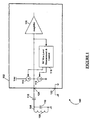
- a transponder is generally indicated by the numeral 100.
- the transponder 100 comprises a high gain signal amplifier 120, current sources 114 and 116, and a DC bias level measurement and control circuit 118 in an integrated circuit package 102; and a parallel tuned circuit 106 comprising a capacitor 110 and an inductor 108, and a DC blocking capacitor 112 connected between an input-output pin 124 of the integrated circuit package 102 and the parallel tuned circuit 106.
- the signal return of the parallel tuned circuit 106 is through a common power or ground pin 122 (ground pin illustrated). However, the use of a common power pin for a signal return is also contemplated and within the scope of the present invention).
- the DC blocking capacitor 112 allows an independent DC bias level to be set at the input of the amplifier 120.
- the DC bias level measurement and control circuit 118 controls the current sources 114 and 116 so that a preferred DC bias value is applied to the amplifier 120 to optimize the available signal amplification thereof.
- the DC bias level measurement and control circuit 118 can also control the gain of the amplifier 120 by changing its DC bias value.
- the amplification of the amplifier 120 may be optimized to receive signals of 1 millivolt or greater.
- the parallel tuned circuit 106 is adapted to receive electromagnetic or radio frequency (RF) energy from a signal source.
- the received energy is in the form of an alternating current (AC) signal which is coupled through the blocking capacitor 112 and amplified by the amplifier 120.
- the amplified signal from the output of the amplifier 120 is then detected (demodulated) as information for processing in logic circuits (not illustrated).
- the blocking capacitor 112 has an AC impedance substantially lower than the input impedance of the amplifier 120. Thus, the blocking capacitor 112 introduces very little attenuation of the received AC signal at the parallel tuned circuit 106.
- a transponder is generally indicated by the numeral 200.
- the transponder 200 comprises a high gain signal amplifier 120, current sources 114 and 116, and a DC bias level measurement and control circuit 118 in an integrated circuit package 102; and a parallel tuned circuit 206 comprising a capacitor 110a, an inductor 108 and a DC blocking capacitor 112a connected in series with the inductor 108.
- the parallel tuned circuit 206 is connected to the input-output pin 124 of the integrated circuit package 102, and the signal return of the parallel tuned circuit 206 is through a common power or ground pin 122 (ground pin illustrated).
- ground pin ground pin illustrated
- the use of a common power pin for a signal return is also contemplated and within the scope of the present invention).
- the DC blocking capacitor 112a allows an independent DC bias level to be set at the input of the amplifier 120, and the DC bias level measurement and control circuit 118 controls the current sources 114 and 116 as disclosed hereinabove.
- the parallel tuned circuit 206 is adapted to receive electromagnetic or radio frequency (RF) energy from a signal source. The received energy is in the form of an alternating current (AC) signal which is coupled through the blocking capacitor 112 and amplified by the amplifier 120. The amplified signal from the output of the amplifier 120 is then detected (demodulated) as information for processing in logic circuits (not illustrated).
- the blocking capacitor 112a has an AC impedance substantially lower than the input impedance of the amplifier 120 and the AC impedance of the capacitor 110a.
- the blocking capacitor 112 introduces very little attenuation of the received AC signal at the parallel tuned circuit 206 and does not materially affect the resonant frequency of the parallel tuned circuit 206.
- the blocking capacitor may also be connected between a parallel connected tuned circuit 206a and common or ground, as indicated in Figure 2.
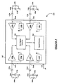
- a transponder having a plurality of signal inputs is generally indicated by the numeral 300.
- the transponder 300 comprises high gain signal amplifiers 120a-120d, DC bias level measurement and control circuits 118a-118d, (current sources 114a-114d and 116a-116d are not illustrated for clarity), a best signal selection circuit 326 and a signal detector 328 in an integrated circuit package 302; and parallel tuned circuits 106a-106d, and DC blocking capacitors 112a-112d connected between input-output pins 124a-124d of the integrated circuit package 302 and the parallel tuned circuits 106a-106d.
- the parallel tuned circuits 106a-106d comprise capacitors 110a-110d and inductors 108a-108d.
- the signal returns of the parallel tuned circuits 106a-106d are through a common power or ground pin 122 (ground pin illustrated). However, the use of a common power pin for a signal return is also contemplated and within the scope of the present invention).
- the DC blocking capacitors 112a-112d allow independent DC bias levels to be set at the inputs of each of the amplifiers 120a-120d.
- the DC bias level measurement and control circuits 118a-118d control the current sources 114a-114d and 116a-116d (not illustrated), respectively, so that preferred DC bias values are applied to the amplifiers 120a-120d to optimize the available signal amplification thereof.
- the DC bias level measurement and control circuits 118a-118d can also control the gain of the amplifiers 120a-120d, respectively, by changing the respective DC bias values thereof.
- the amplification of the amplifiers 120a-120d may be optimized to receive signals of 1 millivolt or greater.
- the parallel tuned circuits 106a-106d are adapted to receive electromagnetic or radio frequency (RF) energy from a signal source(s).
- the received energy is in the form of an alternating current (AC) signal which is coupled through the blocking capacitors 112a-112d and amplified by the amplifiers 120a-120d.
- the amplified signals from the outputs of the amplifiers 120a-120d are compared in the best signal selection circuit 326, wherein the best (i.e., strongest) signal is selected and then detected (demodulated) in the signal detector 328.
- the detected information is processed in logic circuits (not illustrated).
- the blocking capacitors 112a-112d each have an AC impedance substantially lower than the input impedance of the amplifiers 120a-120d.
- the blocking capacitors 112a-112d introduce very little attenuation of the received AC signals at the parallel tuned circuits 106a-106d.
- Four tuned circuits and amplifiers are illustrated for clarity, however, it is contemplated and within the scope of the present invention that any number of tuned circuits and amplifiers may be utilized by the embodiment of the present invention.
- a transponder having a plurality of signal inputs for a plurality of different channels is generally indicated by the numeral 400.
- the transponder 400 comprises high gain signal amplifiers 120a-120d, DC bias level measurement and control circuits 118a-118d, (current sources 114a-114d and 116a-116d are not illustrated for clarity) and signal detectors 428a-428d in an integrated circuit package 402; parallel tuned circuits 106a-106d, and DC blocking capacitors 112a-112d connected between input-output pins 124a-124d of the integrated circuit package 402 and the parallel tuned circuits 106a-106d.
- the parallel tuned circuits 106a-106d comprise capacitors 110a-110d and inductors 108a-108d.
- the signal returns of the parallel tuned circuits 106a-106d are through a common power or ground pin 122 (ground pin illustrated). However, the use of a common power pin for a signal return is also contemplated and within the scope of the present invention).
- the DC blocking capacitors 112a-112d allow independent DC bias levels to be set at the inputs of each of the amplifiers 120a-120d.
- the DC bias level measurement and control circuits 118a-118d control the current sources 114a-114d and 116a-116d (not illustrated), respectively, so that preferred DC bias values are applied to the amplifiers 120a-120d to optimize the available signal amplification thereof.
- the DC bias level measurement and control circuits 118a-118d can also control the gain of the amplifiers 120a-120d, respectively, by changing the respective DC bias values thereof.
- the amplification of the amplifiers 120a-120d may be optimized to receive signals of 1 millivolt or greater.
- the parallel tuned circuits 106a-106d are adapted to receive electromagnetic or radio frequency (RF) energy from a plurality of signal sources which may be at different operating frequencies and contain independent information from each of the plurality of signal sources.
- the received energies are in the form of alternating current (AC) signals which are coupled through the blocking capacitors 112a-112d and amplified by the amplifiers 120a-120d.
- the amplified signals from the outputs of the amplifiers 120a-120d are detected (demodulated) in the signal detectors 428a-428d.
- the demodulated information signals from the signal detectors 428a-428d are processed in logic circuits (not illustrated). Four information channels are illustrated for clarity, however, it is contemplated and within the scope of the present invention that any number of information channels may be received and processed by an embodiment of the present invention.
- the blocking capacitors 112a-112d each have an AC impedance substantially lower than the input impedance of the amplifiers 120a-120d. Thus, the blocking capacitors 112a-112d introduce very little attenuation of the received AC signals at the parallel tuned circuits 106a-106d.
- a generally secured environment having an embodiment of the present invention is represented by the numeral 500.
- the environment 500 may be an automobile, office building, garage with a remotely controlled access gate, warehouse, boat, plane or train, i.e., anything which is secured by a locked entrance and allows access by authorized personnel.
- Signal pickup sensors 552a-552d represent herein the tuned parallel circuits 106a-106d, respectively, of the embodiments disclosed hereinabove.
- a space diversity receiving system may be implemented using the embodiment illustrated in Figure 3 and disclosed hereinabove, by placing the signal pickup sensors 552a-552d (tuned parallel circuits 106a-106d) at various locations on the environment 500.
- This space diversity system allows better reception of, for example but not limitation, a keyless entry system to the environment 500 no matter where the keyless transmitter is in relation to the environment 500.
- the signal pickup sensors 552a-552d may also be utilized with the embodiment of the invention illustrated in Figure 4 and disclosed hereinabove.
- transponder security system which may benefit from the embodiments of the present invention is described more fully in the KEELOQ ® (a registered trademark of Microchip Technology Inc.) products, and more specifically, in the device entitled "Code Hopping Encoder and Transponder," part number HCS412 by Microchip Technology Inc., more fully described in Specification DS41099A (1999) available at http://www.microchip.com, and incorporated by reference herein.
- the HCS412 requires two dedicated package pins for connection to a parallel tuned circuit, as illustrated in Figure 2-2 of the HCS412 data sheet.
- the present invention maintains the functionality of the HCS412 but reduces the number of pins required for external connections to the integrated circuit package.
- the transponder embodiment of Figure 6 is generally indicated by the numeral 600.
- the transponder 600 further comprises a switch 654, for example but not limitation, metal oxide field effect transistors (MOSFET) and a transmitter-modulator circuit 656 in the integrated circuit package 602.
- the switch 654 transfers connection of the input-output pin 124 to either the input of the amplifier 120 for receiving a signal picked up on the turned circuit 106, or to the transmitter-modulator 656 for transmitting a digitally encoded signal from the tuned circuit 106.
- the transponder function of interrogation and acknowledgement is performed by the transponder using the same pin 124 and tuned circuit 106 for an antenna.
- a separate transmitting antenna and pin on the integrated circuit package may be used, i.e., the receiver and transmitter frequencies are different.
- the present invention allows better utilization of the fixed number of pins on an integrated circuit package, thus, enabling more features to be offered for a given integrated circuit package size.
Landscapes
- Engineering & Computer Science (AREA)
- Power Engineering (AREA)
- Microelectronics & Electronic Packaging (AREA)
- Computer Networks & Wireless Communication (AREA)
- Signal Processing (AREA)
- Amplifiers (AREA)
- Input Circuits Of Receivers And Coupling Of Receivers And Audio Equipment (AREA)
- Electronic Switches (AREA)
- Radar Systems Or Details Thereof (AREA)
Claims (19)
- Hochfrequenztransponder, umfassend:eine auf Hochfrequenz abgestimmte Schaltung (106), die ein erstes und ein zweites Ende aufweist;einen ersten Kondensator (112);eine integrierte Schaltung (102), die einen Hochfrequenzverstärker (120) aufweist, wobei besagte integrierte Schaltung (102) einen Signalanschluss (124) und einen gemeinsamen Anschluss (122) aufweist; wobeiein Eingang des besagten Hochfrequenzverstärkers (120) mit besagtem Signalanschluss (124) verbunden ist;besagter erster Kondensator (112) zwischen das erste Ende der besagten auf Hochfrequenz abgestimmten Schaltung (106) und den besagten Signalanschluss (124) geschaltet ist; unddas zweite Ende der besagten auf Hochfrequenz abgestimmten Schaltung (106) mit besagtem gemeinsamem Anschluss (122) verbunden ist, wobeibesagte integrierte Schaltung (102) gekennzeichnet ist durcherste und zweite Stromquellen (114, 116), die mit besagtem Hochfrequenzverstärker (120) verbunden sind, um den Gleichspannungsbiaswert des Verstärkers (120) zu ändern; undeinen Biassteuerungsschaltkreis (118);wobei besagter Biassteuerungsschaltkreis (118) zur Steuerung des Biaspegels mit besagten ersten und zweiten Stromquellen (114, 116) verbunden ist.
- Hochfrequenztransponder gemäß Anspruch 1, wobei besagte abgestimmte Schaltung (106) ein induktives Bauelement (108) und einen zweiten Kondensator (110) umfasst, die parallel verbunden sind.
- Hochfrequenztransponder gemäß Anspruch 1, wobei besagte erste und zweite Stromquellen (114, 116) in Reihe und mit dem Eingang des besagten Hochfrequenzverstärkers (120) verbunden sind.
- Hochfrequenztransponder gemäß Anspruch 3, wobei besagte erste Stromquelle (114) mit einer Betriebsspannung (Vdd) der integrierten Schaltung verbunden ist und besagte zweite Stromquelle (116) mit dem gemeinsamen Anschluss der besagten integrierten Schaltung (102) verbunden ist.
- Hochfrequenztransponder gemäß Anspruch 1, wobei besagte erste Kondensatorimpedanz bei einer erwünschten Frequenz etwa ein Zehntel der Impedanz der besagten auf Hochfrequenz abgestimmten Schaltung (106) bei der erwünschten Frequenz beträgt.
- Hochfrequenztransponder gemäß Anspruch 1, wobei besagte erste Kondensatorimpedanz bei einer erwünschten Frequenz beträchtlich kleiner ist als der Eingangwiderstand des besagten Hochfrequenzverstärkers (106).
- Hochfrequenztransponder gemäß Anspruch 1, wobei besagte auf Hochfrequenz abgestimmte Schaltung (106) in einem erwünschten Abstand von besagter integrierter Schaltung (102) angeordnet ist.
- Hochfrequenztransponder, umfassend:eine auf Hochfrequenz abgestimmte Schaltung (106), die ein erstes und ein zweites Ende aufweist;einen ersten Kondensator (112);eine integrierte Schaltung (102), die einen Hochfrequenzverstärker (120) aufweist; wobeibesagte integrierte Schaltung (102) einen Signalanschluss (124) und einen gemeinsamen Anschluss (122) aufweist;ein Eingang des besagten Hochfrequenzverstärkers (120) mit besagtem Signalanschluss (124) verbunden ist; undbesagte auf Hochfrequenz abgestimmte Schaltung (106) und besagter erster Kondensator (112) so verbunden sind, dass besagter Signalanschluss keinen Gleichstrompfad außerhalb der besagten integrierten Schaltung (102) aufweist,besagte integrierte Schaltung (102) gekennzeichnet ist durcherste und zweite Stromquellen (114, 116), die mit besagtem Hochfrequenzverstärker (120) verbunden sind, um den Gleichspannungsvorspannungswert des Verstärkers (120) zu ändern; undeinen Biassteuerungsschaltkreis (118);wobei besagter Biassteuerungsschaltkreis (118) mit besagten ersten und zweiten Stromquellen (114, 116) verbunden ist, um den Biaspegel zu steuern.
- Hochfrequenztransponder gemäß Anspruch 8, wobei besagte abgestimmte Schaltung ein induktives Bauelement (108) und einen zweiten Kondensator (110) umfasst, die parallel angeschlossen sind.
- Hochfrequenztransponder gemäß Anspruch 9, wobei ein Ende der parallelen Verbindung des besagten induktiven Bauelements (108) und des besagt zweiten Kondensators (110a) an besagten Signalanschluss (124) angeschlossen ist, und besagter erster Kondensator (112a) zwischen besagtem gemeinsamem Anschluss (122) und einem anderen Ende der parallelen Verbindung von besagtem induktivem Bauelement (108) und besagtem zweitem Kondensator (110a) angeschlossen ist
- Hochfrequenztransponder gemäß Anspruch 8, wobei besagte abgestimmte Schaltung ein in Reihe mit besagtem erstem Kondensator (112a) verbundenes induktives Bauelement (108) umfasst, und die daraus resultierende Reihenschaltung parallel mit einem zweiten Kondensator (110a) verbunden ist.
- Hochfrequenztransponder, umfassend:eine Vielzahl von auf Hochfrequenz abgestimmten Schaltungen (106a-d), wobei jede von besagter Vielzahl von auf Hochfrequenz abgestimmten Schaltungen (106a-d) ein erstes und ein zweites Ende aufweist;eine Vielzahl von ersten Kondensatoren (112a-d);eine integrierte Schaltung (302), die eine Vielzahl von Hochfrequenzverstärkern (120a-d), eine Vielzahl von ersten und zweiten Stromquellen, und eine Vielzahl von Vorspannungssteuerungsschaltkreisen (118a-d) aufweist; wobeijede von besagter Vielzahl von ersten und zweiten Stromquellen mit einem entsprechenden von besagter Vielzahl von Hochfrequenzverstärkern (120a-d) verbunden ist, um den Gleichspannungsbiaswert des jeweiligen Verstärkers (120a-d) zu ändern;jeder von besagter Vielzahl von Biassteuerungsschaltkreisen (118a-d) mit einer jeweiligen von besagten ersten und zweiten Stromquellen verbunden ist, um die Biaspegel von diesen zu steuern;besagte integrierte Schaltung (302) eine Vielzahl von Signalanschlüssen (124a-d) und einen gemeinsamer Anschluss (122) aufweist;ein Eingang von jedem der besagten Vielzahl von Hochfrequenzverstärkern (10a-d) mit einem jeweiligen von besagter Vielzahl von Signalanschlüssen (124a-d) verbunden ist;jeder von besagter Vielzahl von ersten Kondensatoren (112a-d) zwischen das erste Ende einer jeweiligen von besagter Vielzahl von auf Hochfrequenz abgestimmten Schaltungen (106a-d) und der jeweiligen von besagter Vielzahl von Signalanschlüssen (124a-d) geschaltet ist; unddas zweite Ende von jeder von besagter Vielzahl von auf Hochfrequenz abgestimmten Schaltungen (106a-d) mit besagtem gemeinsamem Anschluss (122) verbunden ist.
- Hochfrequenztransponder gemäß Anspruch 12, wobei jede von besagter Vielzahl von abgestimmten Schaltungen (106a-d) ein induktives Bauelement (108a) und einen zweiten Kondensator (110a) umfasst, die parallel verbunden sind.
- Hochfrequenztransponder gemäß Anspruch 12, wobei besagte Vielzahl von auf Hochfrequenz abgestimmten Schaltungen (106a-d) in einem erwünschten Abstand von besagter integrierter Schaltung (302) angeordnet ist.
- Hochfrequenztransponder gemäß Anspruch 12, weiterhin umfassend:einen Bestsignalauswahlschaltkreis (326), der mit Signalausgängen von besagter Vielzahl von Hochfrequenzverstärkern (120a-d) verbunden ist; undeinen Signaldetektor (328), der mit einem Ausgang des besagten Bestsignalauswahlschaltkreises (326) verbunden ist,wobei ein Bestsignal von den Ausgängen besagter Vielzahl von Hochfrequenzverstärkern (120a-d) ausgewählt wird.
- Hochfrequenztransponder gemäß Anspruch 12, wobei besagte Vielzahl von auf Hochfrequenz abgestimmten Schaltungen (106a) auf dieselbe Frequenz abgestimmt ist.
- Hochfrequenztransponder gemäß Anspruch 12, wobei besagte Vielzahl von auf Hochfrequenz abgestimmten Schaltungen (106a-d) auf unterschiedliche Frequenzen abgestimmt ist.
- Hochfrequenztransponder gemäß Anspruch 11, weiterhin umfassend eine Vielzahl von Signaldetektoren (428a-d), wobei jeder von besagter Vielzahl von Signaldetektoren (428a-d) mit einem Ausgang eines jeweiligen von besagter Vielzahl von Hochfrequenzverstärkern (120a-d) verbunden ist.
- Hochfrequenztransponder gemäß Anspruch 1, weiterhin umfassend:einen Signalschalter (654), der zwischen besagtem Signalanschluss (124) und dem Eingang des besagten Hochfrequenzverstärkers (120) angeschlossen ist; undeinen Transmitter-Modulator (656), der mit besagtem Signalschalter (654) verbunden ist, wobei besagter Signalschalter (654) besagten Transmitter-Modulator (656) mit besagtem Signalanschluss (124) verbindet und den Eingang des besagten Hochfrequenzverstärkers (120) von besagtem Signalanschluss trennt, wenn besagter Transmitter-Modulator (656) ein Signal überträgt.
Applications Claiming Priority (2)
| Application Number | Priority Date | Filing Date | Title |
|---|---|---|---|
| US405451 | 1999-09-24 | ||
| US09/405,451 US6509825B1 (en) | 1999-09-24 | 1999-09-24 | Integrated circuit device having a self-biased, single pin radio frequency signal input |
Publications (3)
| Publication Number | Publication Date |
|---|---|
| EP1087522A2 EP1087522A2 (de) | 2001-03-28 |
| EP1087522A3 EP1087522A3 (de) | 2003-04-02 |
| EP1087522B1 true EP1087522B1 (de) | 2008-01-02 |
Family
ID=23603755
Family Applications (1)
| Application Number | Title | Priority Date | Filing Date |
|---|---|---|---|
| EP00120633A Expired - Lifetime EP1087522B1 (de) | 1999-09-24 | 2000-09-21 | Eine integrierte Schaltung mit selbstpolarisierendem HF-Signalanschluss |
Country Status (9)
| Country | Link |
|---|---|
| US (1) | US6509825B1 (de) |
| EP (1) | EP1087522B1 (de) |
| JP (1) | JP2001136099A (de) |
| KR (1) | KR20010050637A (de) |
| CN (1) | CN1291004A (de) |
| AT (1) | ATE382982T1 (de) |
| BR (1) | BR0004417A (de) |
| DE (1) | DE60037625T2 (de) |
| TW (1) | TW487891B (de) |
Families Citing this family (17)
| Publication number | Priority date | Publication date | Assignee | Title |
|---|---|---|---|---|
| US20020167336A1 (en) * | 2001-05-09 | 2002-11-14 | Jamieson J. Scott | Microprocessor circuit for allowing input and output via a single pin |
| GB2388157A (en) * | 2002-04-02 | 2003-11-05 | Kenneth Marden Henfrey | Motorised door assembly that opens, closes and locks |
| US7526260B2 (en) * | 2002-11-14 | 2009-04-28 | M/A-Com Eurotec, B.V. | Apparatus, methods and articles of manufacture for linear signal modification |
| US6891432B2 (en) * | 2002-11-14 | 2005-05-10 | Mia-Com, Inc. | Apparatus, methods and articles of manufacture for electromagnetic processing |
| CN1723587A (zh) * | 2002-11-07 | 2006-01-18 | 碎云股份有限公司 | 含微型天线的集成电路封装 |
| US20050237161A1 (en) * | 2004-04-23 | 2005-10-27 | Microchip Technology Incorporated | Programmable selective wake-up for radio frequency transponder |
| US7602274B2 (en) * | 2004-04-23 | 2009-10-13 | Microchip Technology Incorporated | Dynamic configuration of a radio frequency transponder |
| US20050237160A1 (en) * | 2004-04-23 | 2005-10-27 | Microchip Technology Incorporated | Reducing false wake-up in a low frequency transponder |
| WO2006008180A1 (en) * | 2004-07-23 | 2006-01-26 | Fractus S.A. | Antenna in package with reduced electromagnetic interaction with on chip elements |
| JP2006157230A (ja) * | 2004-11-26 | 2006-06-15 | Asuka Electron Kk | データ搬送回路 |
| US7956721B2 (en) * | 2007-01-09 | 2011-06-07 | Homerun Holdings Corporation | Power conserving mobile transmitter |
| CN101141427B (zh) * | 2007-03-15 | 2011-09-21 | 中兴通讯股份有限公司 | 一种利用同步时钟信号对数字信号进行解调的方法和装置 |
| US20110050389A1 (en) * | 2009-07-26 | 2011-03-03 | AEQUITAS Innovation | Low power wireless controller systems and methods |
| DE102012107818A1 (de) * | 2012-08-24 | 2014-03-13 | Endress + Hauser Flowtec Ag | Schaltung zur Signalübertragung und zur galvanischen Trennung |
| JP6648515B2 (ja) * | 2015-12-21 | 2020-02-14 | カシオ計算機株式会社 | 電子機器及びその角速度取得方法、角速度取得プログラム |
| US9964985B1 (en) * | 2017-04-07 | 2018-05-08 | Realtek Semiconductor Corp. | Radio frequency power amplifier and method thereof |
| CN112436848B (zh) * | 2020-12-04 | 2022-08-05 | 深圳市锐尔觅移动通信有限公司 | 调谐电路、射频电路及电子设备 |
Family Cites Families (8)
| Publication number | Priority date | Publication date | Assignee | Title |
|---|---|---|---|---|
| FR2662876B1 (fr) * | 1990-05-29 | 1994-04-29 | Fontaine Sa | Recepteur d'ondes radioelectriques a boucle d'induction et a extremement faible consommation, en particulier pour telecommande. |
| JPH08186490A (ja) * | 1994-11-04 | 1996-07-16 | Fujitsu Ltd | 位相同期回路及びデータ再生装置 |
| US5606323A (en) * | 1995-08-31 | 1997-02-25 | International Business Machines Corporation | Diode modulator for radio frequency transponder |
| US5686864A (en) * | 1995-09-05 | 1997-11-11 | Motorola, Inc. | Method and apparatus for controlling a voltage controlled oscillator tuning range in a frequency synthesizer |
| US6130602A (en) * | 1996-05-13 | 2000-10-10 | Micron Technology, Inc. | Radio frequency data communications device |
| US5736902A (en) * | 1996-07-19 | 1998-04-07 | Maxim Integrated Products, Inc. | High-gain common-emitter output stage |
| JP3657079B2 (ja) * | 1997-03-19 | 2005-06-08 | 富士通株式会社 | エンハンスメント型トランジスタ回路のバイアス回路を有する集積回路装置 |
| US6516182B1 (en) * | 1998-12-21 | 2003-02-04 | Microchip Technology Incorporated | High gain input stage for a radio frequency identification (RFID) transponder and method therefor |
-
1999
- 1999-09-24 US US09/405,451 patent/US6509825B1/en not_active Expired - Lifetime
-
2000
- 2000-09-21 DE DE60037625T patent/DE60037625T2/de not_active Expired - Lifetime
- 2000-09-21 EP EP00120633A patent/EP1087522B1/de not_active Expired - Lifetime
- 2000-09-21 AT AT00120633T patent/ATE382982T1/de not_active IP Right Cessation
- 2000-09-24 CN CN00131372A patent/CN1291004A/zh active Pending
- 2000-09-25 BR BR0004417-2A patent/BR0004417A/pt not_active Application Discontinuation
- 2000-09-25 JP JP2000291328A patent/JP2001136099A/ja not_active Withdrawn
- 2000-09-25 KR KR1020000056261A patent/KR20010050637A/ko not_active Application Discontinuation
-
2001
- 2001-01-10 TW TW089119778A patent/TW487891B/zh not_active IP Right Cessation
Non-Patent Citations (1)
| Title |
|---|
| None * |
Also Published As
| Publication number | Publication date |
|---|---|
| DE60037625T2 (de) | 2008-12-24 |
| DE60037625D1 (de) | 2008-02-14 |
| US6509825B1 (en) | 2003-01-21 |
| BR0004417A (pt) | 2001-10-23 |
| EP1087522A2 (de) | 2001-03-28 |
| JP2001136099A (ja) | 2001-05-18 |
| KR20010050637A (ko) | 2001-06-15 |
| ATE382982T1 (de) | 2008-01-15 |
| TW487891B (en) | 2002-05-21 |
| CN1291004A (zh) | 2001-04-11 |
| EP1087522A3 (de) | 2003-04-02 |
Similar Documents
| Publication | Publication Date | Title |
|---|---|---|
| EP1087522B1 (de) | Eine integrierte Schaltung mit selbstpolarisierendem HF-Signalanschluss | |
| US7158771B2 (en) | Integrated circuit transponder having a plurality of high-gain radio frequency signal inputs | |
| US4600829A (en) | Electronic proximity identification and recognition system with isolated two-way coupling | |
| EP1454294B1 (de) | Drahtgebundene schnittstelle zu einem drahtlosen kommunikationsgerät | |
| EP2070198B1 (de) | Funkfrequenzidentifikations-lesegerät mit einem signalunterdrücker und verfahren dafür | |
| US4654658A (en) | Identification system with vector phase angle detection | |
| US5591951A (en) | System and method for simultaneously collecting serial number information from numerous identity tags | |
| US7023321B2 (en) | Transmitting and receiving method, especially for detecting an ID transmitter | |
| US20080001754A1 (en) | Wireless Communication Systems, Interrogators and Methods of Communicating Within a Wireless Communication System | |
| US20080238623A1 (en) | Transceiver front-end having tx and rx isolation | |
| KR19980032717A (ko) | 키없는 원격 엔트리 시스템을 위한 트랜스폰더 | |
| US7014103B2 (en) | Differential radio frequency identification reader | |
| CN101091197A (zh) | 从rfid装置检测eas功能的eas阅读器 | |
| US20060208855A1 (en) | In-vehicle receiver having interior and exterior antennas | |
| US12073279B2 (en) | Access system | |
| US7259673B2 (en) | Anti-theft arrangement, method and program | |
| US20020075134A1 (en) | Intelligent signal switch/detector | |
| CN217157308U (zh) | 一种小型化报到装置 | |
| CN213904417U (zh) | 一种免钥匙触发装置、门禁装置及电梯控制装置 | |
| US5191345A (en) | Circuit to increase the information bit rate in a system for the exchange of data | |
| KR20230014917A (ko) | 잔류신호 저감 기법을 사용한 근거리 통신 불능 영역 제거 기능을 갖는 rfid 리더 | |
| EP1688871B1 (de) | Zusammenschaltung drahtloser Kommunikationsvorrichtungen | |
| JPH05174221A (ja) | 入出管理用ゲート | |
| JPS6314969A (ja) | キ−レス・エントリ−装置 |
Legal Events
| Date | Code | Title | Description |
|---|---|---|---|
| PUAI | Public reference made under article 153(3) epc to a published international application that has entered the european phase |
Free format text: ORIGINAL CODE: 0009012 |
|
| 17P | Request for examination filed |
Effective date: 20000922 |
|
| AK | Designated contracting states |
Kind code of ref document: A2 Designated state(s): AT BE CH CY DE DK ES FI FR GB GR IE IT LI LU MC NL PT SE |
|
| AX | Request for extension of the european patent |
Free format text: AL;LT;LV;MK;RO;SI |
|
| PUAL | Search report despatched |
Free format text: ORIGINAL CODE: 0009013 |
|
| AK | Designated contracting states |
Designated state(s): AT BE CH CY DE DK ES FI FR GB GR IE IT LI LU MC NL PT SE Kind code of ref document: A3 Designated state(s): AT BE CH CY DE DK ES FI FR GB GR IE IT LI LU MC NL PT SE |
|
| AX | Request for extension of the european patent |
Extension state: AL LT LV MK RO SI |
|
| RIC1 | Information provided on ipc code assigned before grant |
Ipc: 7G 06K 19/07 B Ipc: 7H 03F 3/45 A |
|
| AKX | Designation fees paid |
Designated state(s): AT BE CH CY DE DK ES FI FR GB GR IE IT LI LU MC NL PT SE |
|
| GRAP | Despatch of communication of intention to grant a patent |
Free format text: ORIGINAL CODE: EPIDOSNIGR1 |
|
| GRAS | Grant fee paid |
Free format text: ORIGINAL CODE: EPIDOSNIGR3 |
|
| GRAA | (expected) grant |
Free format text: ORIGINAL CODE: 0009210 |
|
| AK | Designated contracting states |
Kind code of ref document: B1 Designated state(s): AT BE CH CY DE DK ES FI FR GB GR IE IT LI LU MC NL PT SE |
|
| REG | Reference to a national code |
Ref country code: GB Ref legal event code: FG4D |
|
| REG | Reference to a national code |
Ref country code: IE Ref legal event code: FG4D |
|
| REG | Reference to a national code |
Ref country code: CH Ref legal event code: EP |
|
| REF | Corresponds to: |
Ref document number: 60037625 Country of ref document: DE Date of ref document: 20080214 Kind code of ref document: P |
|
| PG25 | Lapsed in a contracting state [announced via postgrant information from national office to epo] |
Ref country code: ES Free format text: LAPSE BECAUSE OF FAILURE TO SUBMIT A TRANSLATION OF THE DESCRIPTION OR TO PAY THE FEE WITHIN THE PRESCRIBED TIME-LIMIT Effective date: 20080413 Ref country code: FI Free format text: LAPSE BECAUSE OF FAILURE TO SUBMIT A TRANSLATION OF THE DESCRIPTION OR TO PAY THE FEE WITHIN THE PRESCRIBED TIME-LIMIT Effective date: 20080102 Ref country code: LI Free format text: LAPSE BECAUSE OF FAILURE TO SUBMIT A TRANSLATION OF THE DESCRIPTION OR TO PAY THE FEE WITHIN THE PRESCRIBED TIME-LIMIT Effective date: 20080102 Ref country code: CH Free format text: LAPSE BECAUSE OF FAILURE TO SUBMIT A TRANSLATION OF THE DESCRIPTION OR TO PAY THE FEE WITHIN THE PRESCRIBED TIME-LIMIT Effective date: 20080102 |
|
| REG | Reference to a national code |
Ref country code: CH Ref legal event code: PL |
|
| PG25 | Lapsed in a contracting state [announced via postgrant information from national office to epo] |
Ref country code: AT Free format text: LAPSE BECAUSE OF FAILURE TO SUBMIT A TRANSLATION OF THE DESCRIPTION OR TO PAY THE FEE WITHIN THE PRESCRIBED TIME-LIMIT Effective date: 20080102 |
|
| ET | Fr: translation filed | ||
| PG25 | Lapsed in a contracting state [announced via postgrant information from national office to epo] |
Ref country code: PT Free format text: LAPSE BECAUSE OF FAILURE TO SUBMIT A TRANSLATION OF THE DESCRIPTION OR TO PAY THE FEE WITHIN THE PRESCRIBED TIME-LIMIT Effective date: 20080602 Ref country code: BE Free format text: LAPSE BECAUSE OF FAILURE TO SUBMIT A TRANSLATION OF THE DESCRIPTION OR TO PAY THE FEE WITHIN THE PRESCRIBED TIME-LIMIT Effective date: 20080102 |
|
| PG25 | Lapsed in a contracting state [announced via postgrant information from national office to epo] |
Ref country code: SE Free format text: LAPSE BECAUSE OF FAILURE TO SUBMIT A TRANSLATION OF THE DESCRIPTION OR TO PAY THE FEE WITHIN THE PRESCRIBED TIME-LIMIT Effective date: 20080402 Ref country code: DK Free format text: LAPSE BECAUSE OF FAILURE TO SUBMIT A TRANSLATION OF THE DESCRIPTION OR TO PAY THE FEE WITHIN THE PRESCRIBED TIME-LIMIT Effective date: 20080102 |
|
| PLBE | No opposition filed within time limit |
Free format text: ORIGINAL CODE: 0009261 |
|
| STAA | Information on the status of an ep patent application or granted ep patent |
Free format text: STATUS: NO OPPOSITION FILED WITHIN TIME LIMIT |
|
| 26N | No opposition filed |
Effective date: 20081003 |
|
| PG25 | Lapsed in a contracting state [announced via postgrant information from national office to epo] |
Ref country code: MC Free format text: LAPSE BECAUSE OF NON-PAYMENT OF DUE FEES Effective date: 20080930 |
|
| GBPC | Gb: european patent ceased through non-payment of renewal fee |
Effective date: 20080921 |
|
| PG25 | Lapsed in a contracting state [announced via postgrant information from national office to epo] |
Ref country code: IE Free format text: LAPSE BECAUSE OF NON-PAYMENT OF DUE FEES Effective date: 20080922 Ref country code: CY Free format text: LAPSE BECAUSE OF FAILURE TO SUBMIT A TRANSLATION OF THE DESCRIPTION OR TO PAY THE FEE WITHIN THE PRESCRIBED TIME-LIMIT Effective date: 20080102 |
|
| PG25 | Lapsed in a contracting state [announced via postgrant information from national office to epo] |
Ref country code: GB Free format text: LAPSE BECAUSE OF NON-PAYMENT OF DUE FEES Effective date: 20080921 |
|
| PG25 | Lapsed in a contracting state [announced via postgrant information from national office to epo] |
Ref country code: LU Free format text: LAPSE BECAUSE OF NON-PAYMENT OF DUE FEES Effective date: 20080921 |
|
| PG25 | Lapsed in a contracting state [announced via postgrant information from national office to epo] |
Ref country code: GR Free format text: LAPSE BECAUSE OF FAILURE TO SUBMIT A TRANSLATION OF THE DESCRIPTION OR TO PAY THE FEE WITHIN THE PRESCRIBED TIME-LIMIT Effective date: 20080403 |
|
| REG | Reference to a national code |
Ref country code: FR Ref legal event code: PLFP Year of fee payment: 17 |
|
| REG | Reference to a national code |
Ref country code: FR Ref legal event code: PLFP Year of fee payment: 18 |
|
| REG | Reference to a national code |
Ref country code: FR Ref legal event code: PLFP Year of fee payment: 19 |
|
| PGFP | Annual fee paid to national office [announced via postgrant information from national office to epo] |
Ref country code: NL Payment date: 20190826 Year of fee payment: 20 |
|
| PGFP | Annual fee paid to national office [announced via postgrant information from national office to epo] |
Ref country code: FR Payment date: 20190820 Year of fee payment: 20 Ref country code: IT Payment date: 20190829 Year of fee payment: 20 Ref country code: DE Payment date: 20190820 Year of fee payment: 20 |
|
| REG | Reference to a national code |
Ref country code: DE Ref legal event code: R071 Ref document number: 60037625 Country of ref document: DE |
|
| REG | Reference to a national code |
Ref country code: NL Ref legal event code: MK Effective date: 20200920 |