EP1087433A1 - Process for the formation of silicon oxide films - Google Patents
Process for the formation of silicon oxide films Download PDFInfo
- Publication number
- EP1087433A1 EP1087433A1 EP00912923A EP00912923A EP1087433A1 EP 1087433 A1 EP1087433 A1 EP 1087433A1 EP 00912923 A EP00912923 A EP 00912923A EP 00912923 A EP00912923 A EP 00912923A EP 1087433 A1 EP1087433 A1 EP 1087433A1
- Authority
- EP
- European Patent Office
- Prior art keywords
- film
- silicon oxide
- silicon
- oxide film
- polysilane
- Prior art date
- Legal status (The legal status is an assumption and is not a legal conclusion. Google has not performed a legal analysis and makes no representation as to the accuracy of the status listed.)
- Withdrawn
Links
Images

Classifications
-
- H—ELECTRICITY
- H01—ELECTRIC ELEMENTS
- H01L—SEMICONDUCTOR DEVICES NOT COVERED BY CLASS H10
- H01L21/00—Processes or apparatus adapted for the manufacture or treatment of semiconductor or solid state devices or of parts thereof
- H01L21/02—Manufacture or treatment of semiconductor devices or of parts thereof
- H01L21/02104—Forming layers
- H01L21/02107—Forming insulating materials on a substrate
- H01L21/02109—Forming insulating materials on a substrate characterised by the type of layer, e.g. type of material, porous/non-porous, pre-cursors, mixtures or laminates
- H01L21/02112—Forming insulating materials on a substrate characterised by the type of layer, e.g. type of material, porous/non-porous, pre-cursors, mixtures or laminates characterised by the material of the layer
- H01L21/02123—Forming insulating materials on a substrate characterised by the type of layer, e.g. type of material, porous/non-porous, pre-cursors, mixtures or laminates characterised by the material of the layer the material containing silicon
- H01L21/02164—Forming insulating materials on a substrate characterised by the type of layer, e.g. type of material, porous/non-porous, pre-cursors, mixtures or laminates characterised by the material of the layer the material containing silicon the material being a silicon oxide, e.g. SiO2
-
- C—CHEMISTRY; METALLURGY
- C23—COATING METALLIC MATERIAL; COATING MATERIAL WITH METALLIC MATERIAL; CHEMICAL SURFACE TREATMENT; DIFFUSION TREATMENT OF METALLIC MATERIAL; COATING BY VACUUM EVAPORATION, BY SPUTTERING, BY ION IMPLANTATION OR BY CHEMICAL VAPOUR DEPOSITION, IN GENERAL; INHIBITING CORROSION OF METALLIC MATERIAL OR INCRUSTATION IN GENERAL
- C23C—COATING METALLIC MATERIAL; COATING MATERIAL WITH METALLIC MATERIAL; SURFACE TREATMENT OF METALLIC MATERIAL BY DIFFUSION INTO THE SURFACE, BY CHEMICAL CONVERSION OR SUBSTITUTION; COATING BY VACUUM EVAPORATION, BY SPUTTERING, BY ION IMPLANTATION OR BY CHEMICAL VAPOUR DEPOSITION, IN GENERAL
- C23C18/00—Chemical coating by decomposition of either liquid compounds or solutions of the coating forming compounds, without leaving reaction products of surface material in the coating; Contact plating
- C23C18/02—Chemical coating by decomposition of either liquid compounds or solutions of the coating forming compounds, without leaving reaction products of surface material in the coating; Contact plating by thermal decomposition
- C23C18/12—Chemical coating by decomposition of either liquid compounds or solutions of the coating forming compounds, without leaving reaction products of surface material in the coating; Contact plating by thermal decomposition characterised by the deposition of inorganic material other than metallic material
- C23C18/1204—Chemical coating by decomposition of either liquid compounds or solutions of the coating forming compounds, without leaving reaction products of surface material in the coating; Contact plating by thermal decomposition characterised by the deposition of inorganic material other than metallic material inorganic material, e.g. non-oxide and non-metallic such as sulfides, nitrides based compounds
- C23C18/1208—Oxides, e.g. ceramics
- C23C18/1212—Zeolites, glasses
-
- C—CHEMISTRY; METALLURGY
- C23—COATING METALLIC MATERIAL; COATING MATERIAL WITH METALLIC MATERIAL; CHEMICAL SURFACE TREATMENT; DIFFUSION TREATMENT OF METALLIC MATERIAL; COATING BY VACUUM EVAPORATION, BY SPUTTERING, BY ION IMPLANTATION OR BY CHEMICAL VAPOUR DEPOSITION, IN GENERAL; INHIBITING CORROSION OF METALLIC MATERIAL OR INCRUSTATION IN GENERAL
- C23C—COATING METALLIC MATERIAL; COATING MATERIAL WITH METALLIC MATERIAL; SURFACE TREATMENT OF METALLIC MATERIAL BY DIFFUSION INTO THE SURFACE, BY CHEMICAL CONVERSION OR SUBSTITUTION; COATING BY VACUUM EVAPORATION, BY SPUTTERING, BY ION IMPLANTATION OR BY CHEMICAL VAPOUR DEPOSITION, IN GENERAL
- C23C18/00—Chemical coating by decomposition of either liquid compounds or solutions of the coating forming compounds, without leaving reaction products of surface material in the coating; Contact plating
- C23C18/02—Chemical coating by decomposition of either liquid compounds or solutions of the coating forming compounds, without leaving reaction products of surface material in the coating; Contact plating by thermal decomposition
- C23C18/12—Chemical coating by decomposition of either liquid compounds or solutions of the coating forming compounds, without leaving reaction products of surface material in the coating; Contact plating by thermal decomposition characterised by the deposition of inorganic material other than metallic material
- C23C18/1204—Chemical coating by decomposition of either liquid compounds or solutions of the coating forming compounds, without leaving reaction products of surface material in the coating; Contact plating by thermal decomposition characterised by the deposition of inorganic material other than metallic material inorganic material, e.g. non-oxide and non-metallic such as sulfides, nitrides based compounds
- C23C18/122—Inorganic polymers, e.g. silanes, polysilazanes, polysiloxanes
-
- C—CHEMISTRY; METALLURGY
- C23—COATING METALLIC MATERIAL; COATING MATERIAL WITH METALLIC MATERIAL; CHEMICAL SURFACE TREATMENT; DIFFUSION TREATMENT OF METALLIC MATERIAL; COATING BY VACUUM EVAPORATION, BY SPUTTERING, BY ION IMPLANTATION OR BY CHEMICAL VAPOUR DEPOSITION, IN GENERAL; INHIBITING CORROSION OF METALLIC MATERIAL OR INCRUSTATION IN GENERAL
- C23C—COATING METALLIC MATERIAL; COATING MATERIAL WITH METALLIC MATERIAL; SURFACE TREATMENT OF METALLIC MATERIAL BY DIFFUSION INTO THE SURFACE, BY CHEMICAL CONVERSION OR SUBSTITUTION; COATING BY VACUUM EVAPORATION, BY SPUTTERING, BY ION IMPLANTATION OR BY CHEMICAL VAPOUR DEPOSITION, IN GENERAL
- C23C18/00—Chemical coating by decomposition of either liquid compounds or solutions of the coating forming compounds, without leaving reaction products of surface material in the coating; Contact plating
- C23C18/02—Chemical coating by decomposition of either liquid compounds or solutions of the coating forming compounds, without leaving reaction products of surface material in the coating; Contact plating by thermal decomposition
- C23C18/12—Chemical coating by decomposition of either liquid compounds or solutions of the coating forming compounds, without leaving reaction products of surface material in the coating; Contact plating by thermal decomposition characterised by the deposition of inorganic material other than metallic material
- C23C18/125—Process of deposition of the inorganic material
- C23C18/1279—Process of deposition of the inorganic material performed under reactive atmosphere, e.g. oxidising or reducing atmospheres
-
- C—CHEMISTRY; METALLURGY
- C23—COATING METALLIC MATERIAL; COATING MATERIAL WITH METALLIC MATERIAL; CHEMICAL SURFACE TREATMENT; DIFFUSION TREATMENT OF METALLIC MATERIAL; COATING BY VACUUM EVAPORATION, BY SPUTTERING, BY ION IMPLANTATION OR BY CHEMICAL VAPOUR DEPOSITION, IN GENERAL; INHIBITING CORROSION OF METALLIC MATERIAL OR INCRUSTATION IN GENERAL
- C23C—COATING METALLIC MATERIAL; COATING MATERIAL WITH METALLIC MATERIAL; SURFACE TREATMENT OF METALLIC MATERIAL BY DIFFUSION INTO THE SURFACE, BY CHEMICAL CONVERSION OR SUBSTITUTION; COATING BY VACUUM EVAPORATION, BY SPUTTERING, BY ION IMPLANTATION OR BY CHEMICAL VAPOUR DEPOSITION, IN GENERAL
- C23C18/00—Chemical coating by decomposition of either liquid compounds or solutions of the coating forming compounds, without leaving reaction products of surface material in the coating; Contact plating
- C23C18/14—Decomposition by irradiation, e.g. photolysis, particle radiation or by mixed irradiation sources
- C23C18/143—Radiation by light, e.g. photolysis or pyrolysis
-
- H—ELECTRICITY
- H01—ELECTRIC ELEMENTS
- H01L—SEMICONDUCTOR DEVICES NOT COVERED BY CLASS H10
- H01L21/00—Processes or apparatus adapted for the manufacture or treatment of semiconductor or solid state devices or of parts thereof
- H01L21/02—Manufacture or treatment of semiconductor devices or of parts thereof
- H01L21/02104—Forming layers
- H01L21/02107—Forming insulating materials on a substrate
- H01L21/02109—Forming insulating materials on a substrate characterised by the type of layer, e.g. type of material, porous/non-porous, pre-cursors, mixtures or laminates
- H01L21/02205—Forming insulating materials on a substrate characterised by the type of layer, e.g. type of material, porous/non-porous, pre-cursors, mixtures or laminates the layer being characterised by the precursor material for deposition
- H01L21/02208—Forming insulating materials on a substrate characterised by the type of layer, e.g. type of material, porous/non-porous, pre-cursors, mixtures or laminates the layer being characterised by the precursor material for deposition the precursor containing a compound comprising Si
- H01L21/02211—Forming insulating materials on a substrate characterised by the type of layer, e.g. type of material, porous/non-porous, pre-cursors, mixtures or laminates the layer being characterised by the precursor material for deposition the precursor containing a compound comprising Si the compound being a silane, e.g. disilane, methylsilane or chlorosilane
-
- H—ELECTRICITY
- H01—ELECTRIC ELEMENTS
- H01L—SEMICONDUCTOR DEVICES NOT COVERED BY CLASS H10
- H01L21/00—Processes or apparatus adapted for the manufacture or treatment of semiconductor or solid state devices or of parts thereof
- H01L21/02—Manufacture or treatment of semiconductor devices or of parts thereof
- H01L21/02104—Forming layers
- H01L21/02107—Forming insulating materials on a substrate
- H01L21/02225—Forming insulating materials on a substrate characterised by the process for the formation of the insulating layer
- H01L21/02227—Forming insulating materials on a substrate characterised by the process for the formation of the insulating layer formation by a process other than a deposition process
- H01L21/0223—Forming insulating materials on a substrate characterised by the process for the formation of the insulating layer formation by a process other than a deposition process formation by oxidation, e.g. oxidation of the substrate
- H01L21/02233—Forming insulating materials on a substrate characterised by the process for the formation of the insulating layer formation by a process other than a deposition process formation by oxidation, e.g. oxidation of the substrate of the semiconductor substrate or a semiconductor layer
- H01L21/02236—Forming insulating materials on a substrate characterised by the process for the formation of the insulating layer formation by a process other than a deposition process formation by oxidation, e.g. oxidation of the substrate of the semiconductor substrate or a semiconductor layer group IV semiconductor
-
- H—ELECTRICITY
- H01—ELECTRIC ELEMENTS
- H01L—SEMICONDUCTOR DEVICES NOT COVERED BY CLASS H10
- H01L21/00—Processes or apparatus adapted for the manufacture or treatment of semiconductor or solid state devices or of parts thereof
- H01L21/02—Manufacture or treatment of semiconductor devices or of parts thereof
- H01L21/02104—Forming layers
- H01L21/02107—Forming insulating materials on a substrate
- H01L21/02225—Forming insulating materials on a substrate characterised by the process for the formation of the insulating layer
- H01L21/0226—Forming insulating materials on a substrate characterised by the process for the formation of the insulating layer formation by a deposition process
- H01L21/02282—Forming insulating materials on a substrate characterised by the process for the formation of the insulating layer formation by a deposition process liquid deposition, e.g. spin-coating, sol-gel techniques, spray coating
-
- H—ELECTRICITY
- H01—ELECTRIC ELEMENTS
- H01L—SEMICONDUCTOR DEVICES NOT COVERED BY CLASS H10
- H01L21/00—Processes or apparatus adapted for the manufacture or treatment of semiconductor or solid state devices or of parts thereof
- H01L21/02—Manufacture or treatment of semiconductor devices or of parts thereof
- H01L21/02104—Forming layers
- H01L21/02107—Forming insulating materials on a substrate
- H01L21/02296—Forming insulating materials on a substrate characterised by the treatment performed before or after the formation of the layer
- H01L21/02318—Forming insulating materials on a substrate characterised by the treatment performed before or after the formation of the layer post-treatment
- H01L21/02321—Forming insulating materials on a substrate characterised by the treatment performed before or after the formation of the layer post-treatment introduction of substances into an already existing insulating layer
- H01L21/02323—Forming insulating materials on a substrate characterised by the treatment performed before or after the formation of the layer post-treatment introduction of substances into an already existing insulating layer introduction of oxygen
-
- H—ELECTRICITY
- H01—ELECTRIC ELEMENTS
- H01L—SEMICONDUCTOR DEVICES NOT COVERED BY CLASS H10
- H01L21/00—Processes or apparatus adapted for the manufacture or treatment of semiconductor or solid state devices or of parts thereof
- H01L21/02—Manufacture or treatment of semiconductor devices or of parts thereof
- H01L21/02104—Forming layers
- H01L21/02107—Forming insulating materials on a substrate
- H01L21/02296—Forming insulating materials on a substrate characterised by the treatment performed before or after the formation of the layer
- H01L21/02318—Forming insulating materials on a substrate characterised by the treatment performed before or after the formation of the layer post-treatment
- H01L21/02337—Forming insulating materials on a substrate characterised by the treatment performed before or after the formation of the layer post-treatment treatment by exposure to a gas or vapour
-
- H—ELECTRICITY
- H01—ELECTRIC ELEMENTS
- H01L—SEMICONDUCTOR DEVICES NOT COVERED BY CLASS H10
- H01L21/00—Processes or apparatus adapted for the manufacture or treatment of semiconductor or solid state devices or of parts thereof
- H01L21/02—Manufacture or treatment of semiconductor devices or of parts thereof
- H01L21/02104—Forming layers
- H01L21/02107—Forming insulating materials on a substrate
- H01L21/02296—Forming insulating materials on a substrate characterised by the treatment performed before or after the formation of the layer
- H01L21/02318—Forming insulating materials on a substrate characterised by the treatment performed before or after the formation of the layer post-treatment
- H01L21/02345—Forming insulating materials on a substrate characterised by the treatment performed before or after the formation of the layer post-treatment treatment by exposure to radiation, e.g. visible light
-
- H—ELECTRICITY
- H01—ELECTRIC ELEMENTS
- H01L—SEMICONDUCTOR DEVICES NOT COVERED BY CLASS H10
- H01L21/00—Processes or apparatus adapted for the manufacture or treatment of semiconductor or solid state devices or of parts thereof
- H01L21/02—Manufacture or treatment of semiconductor devices or of parts thereof
- H01L21/04—Manufacture or treatment of semiconductor devices or of parts thereof the devices having at least one potential-jump barrier or surface barrier, e.g. PN junction, depletion layer or carrier concentration layer
- H01L21/18—Manufacture or treatment of semiconductor devices or of parts thereof the devices having at least one potential-jump barrier or surface barrier, e.g. PN junction, depletion layer or carrier concentration layer the devices having semiconductor bodies comprising elements of Group IV of the Periodic System or AIIIBV compounds with or without impurities, e.g. doping materials
- H01L21/30—Treatment of semiconductor bodies using processes or apparatus not provided for in groups H01L21/20 - H01L21/26
- H01L21/31—Treatment of semiconductor bodies using processes or apparatus not provided for in groups H01L21/20 - H01L21/26 to form insulating layers thereon, e.g. for masking or by using photolithographic techniques; After treatment of these layers; Selection of materials for these layers
- H01L21/312—Organic layers, e.g. photoresist
- H01L21/3121—Layers comprising organo-silicon compounds
-
- H—ELECTRICITY
- H01—ELECTRIC ELEMENTS
- H01L—SEMICONDUCTOR DEVICES NOT COVERED BY CLASS H10
- H01L21/00—Processes or apparatus adapted for the manufacture or treatment of semiconductor or solid state devices or of parts thereof
- H01L21/02—Manufacture or treatment of semiconductor devices or of parts thereof
- H01L21/04—Manufacture or treatment of semiconductor devices or of parts thereof the devices having at least one potential-jump barrier or surface barrier, e.g. PN junction, depletion layer or carrier concentration layer
- H01L21/18—Manufacture or treatment of semiconductor devices or of parts thereof the devices having at least one potential-jump barrier or surface barrier, e.g. PN junction, depletion layer or carrier concentration layer the devices having semiconductor bodies comprising elements of Group IV of the Periodic System or AIIIBV compounds with or without impurities, e.g. doping materials
- H01L21/30—Treatment of semiconductor bodies using processes or apparatus not provided for in groups H01L21/20 - H01L21/26
- H01L21/31—Treatment of semiconductor bodies using processes or apparatus not provided for in groups H01L21/20 - H01L21/26 to form insulating layers thereon, e.g. for masking or by using photolithographic techniques; After treatment of these layers; Selection of materials for these layers
- H01L21/314—Inorganic layers
- H01L21/316—Inorganic layers composed of oxides or glassy oxides or oxide based glass
-
- H—ELECTRICITY
- H01—ELECTRIC ELEMENTS
- H01L—SEMICONDUCTOR DEVICES NOT COVERED BY CLASS H10
- H01L21/00—Processes or apparatus adapted for the manufacture or treatment of semiconductor or solid state devices or of parts thereof
- H01L21/02—Manufacture or treatment of semiconductor devices or of parts thereof
- H01L21/04—Manufacture or treatment of semiconductor devices or of parts thereof the devices having at least one potential-jump barrier or surface barrier, e.g. PN junction, depletion layer or carrier concentration layer
- H01L21/18—Manufacture or treatment of semiconductor devices or of parts thereof the devices having at least one potential-jump barrier or surface barrier, e.g. PN junction, depletion layer or carrier concentration layer the devices having semiconductor bodies comprising elements of Group IV of the Periodic System or AIIIBV compounds with or without impurities, e.g. doping materials
- H01L21/30—Treatment of semiconductor bodies using processes or apparatus not provided for in groups H01L21/20 - H01L21/26
- H01L21/324—Thermal treatment for modifying the properties of semiconductor bodies, e.g. annealing, sintering
-
- C—CHEMISTRY; METALLURGY
- C23—COATING METALLIC MATERIAL; COATING MATERIAL WITH METALLIC MATERIAL; CHEMICAL SURFACE TREATMENT; DIFFUSION TREATMENT OF METALLIC MATERIAL; COATING BY VACUUM EVAPORATION, BY SPUTTERING, BY ION IMPLANTATION OR BY CHEMICAL VAPOUR DEPOSITION, IN GENERAL; INHIBITING CORROSION OF METALLIC MATERIAL OR INCRUSTATION IN GENERAL
- C23C—COATING METALLIC MATERIAL; COATING MATERIAL WITH METALLIC MATERIAL; SURFACE TREATMENT OF METALLIC MATERIAL BY DIFFUSION INTO THE SURFACE, BY CHEMICAL CONVERSION OR SUBSTITUTION; COATING BY VACUUM EVAPORATION, BY SPUTTERING, BY ION IMPLANTATION OR BY CHEMICAL VAPOUR DEPOSITION, IN GENERAL
- C23C18/00—Chemical coating by decomposition of either liquid compounds or solutions of the coating forming compounds, without leaving reaction products of surface material in the coating; Contact plating
- C23C18/14—Decomposition by irradiation, e.g. photolysis, particle radiation or by mixed irradiation sources
- C23C18/145—Radiation by charged particles, e.g. electron beams or ion irradiation
-
- H—ELECTRICITY
- H01—ELECTRIC ELEMENTS
- H01L—SEMICONDUCTOR DEVICES NOT COVERED BY CLASS H10
- H01L21/00—Processes or apparatus adapted for the manufacture or treatment of semiconductor or solid state devices or of parts thereof
- H01L21/02—Manufacture or treatment of semiconductor devices or of parts thereof
- H01L21/04—Manufacture or treatment of semiconductor devices or of parts thereof the devices having at least one potential-jump barrier or surface barrier, e.g. PN junction, depletion layer or carrier concentration layer
- H01L21/18—Manufacture or treatment of semiconductor devices or of parts thereof the devices having at least one potential-jump barrier or surface barrier, e.g. PN junction, depletion layer or carrier concentration layer the devices having semiconductor bodies comprising elements of Group IV of the Periodic System or AIIIBV compounds with or without impurities, e.g. doping materials
- H01L21/30—Treatment of semiconductor bodies using processes or apparatus not provided for in groups H01L21/20 - H01L21/26
- H01L21/31—Treatment of semiconductor bodies using processes or apparatus not provided for in groups H01L21/20 - H01L21/26 to form insulating layers thereon, e.g. for masking or by using photolithographic techniques; After treatment of these layers; Selection of materials for these layers
- H01L21/312—Organic layers, e.g. photoresist
- H01L21/3121—Layers comprising organo-silicon compounds
- H01L21/3122—Layers comprising organo-silicon compounds layers comprising polysiloxane compounds
Definitions
- the present invention relates to a process for forming a silicon oxide film. More specifically, it relates to a process for forming a silicon oxide film which is useful as an electrical insulating film, dielectric film or protective film as used in LSI, thin-film transistor, photoelectric converter, photosensitive body and the like.
- a silicon oxide film has been frequently used as an electrical insulating film, dielectric film or protective film in silicon devices including a semiconductor.
- processes for forming these silicon oxide films there have been known dry processes such as one comprising thermal oxidizing silicon in the air, one comprising forming the film by plasma CVD using a silane gas or a disilane gas in an oxidizing gas such as oxygen or nitric oxide, and one comprising forming the film directly from quartz by sputtering; and wet processes such as one comprising coating alkoxysilane such as tetraethoxysilane in a partially hydrolyzed sol state on a substrate and thermally decomposing it.
- the above dry processes to form a silicon oxide film have the following problems; that is, (a) since it is a gas phase reaction, the generation of particles of impurities in a gas phase causes the contamination of an apparatus or the inclusion of foreign matters, thereby causing low production yield, (b) since the material is in gaseous form, it is difficult to form a film having a uniform thickness on a substrate whose surface is not smooth, (c) productivity is low because the formation of the film is slow, (d) complicated and expensive radio-frequency generator and vacuum apparatus are required in the case of plasma CVD, and (e) they cannot be easily applied to a substrate having a large area.
- gaseous silicon hydride which is highly toxic and highly reactive is used as the material, it not only is difficult to handle but also requires a sealed vacuum apparatus since it is in gaseous form. In general, these apparatus not only are bulky and expensive but also consume a large amount of energy in a vacuum or plasma system, causing an increase in product cost.
- the above wet process system using a sol-gel reaction is a process which comprises heating a partially hydrolyzed alkoxysilane to cause its dehydration-condensation reaction.
- a sol-gel reaction requires a high temperatures heating, the process cannot be applied to a plastic substrate having low heat resistance.
- JP-B 7-29769 discloses that a silicon oxide film is formed from a film formed of an amic acid containing hydrolyzable silicon atoms by irradiation of ultraviolet light in the presence of ozone.
- a silicon compound containing an amic acid having high heat resistance as an organic component is used as the precursor of the silicon oxide film, the film can be made thick. This process, however, has a point, to be improved, which is low productivity caused by a large amount of ultraviolet light required to oxidize and decompose the organic component.
- a process for forming a silicon oxide film which comprises:
- the polysilane compound in the step (1) of the present invention is represented by the formula Si n R m (wherein n is an integer of 3 or more, m is an integer of n to 2n+2, and a plurality of R's are independently a hydrogen atom or an alkyl group). n is an integer of 3 or more.
- a cyclic silicon compound with n of about 5 to about 20 is preferable as the polysilane compound.
- n is smaller than 5
- the silicon compound itself becomes unstable due to the distortion of the ring and difficult to handle
- n is larger than 20
- solubility attributed to the cohesion of the silicon compound can be recognized, whereby the number of solvents that can be selected becomes smaller disadvantageously.
- the plurality of R's are independently a hydrogen atom or an alkyl group.
- alkyl group examples include linear, branched or cyclic alkyl groups having 1 to 10 carbon atoms such as methyl, ethyl, n-propyl, i-propyl, n-butyl, sec-butyl, t-butyl, n-pentyl, i-pentyl, neo-pentyl, n-hexyl, cyclohexyl, n-heptyl, n-octyl, n-nonyl and n-decyl groups.
- a polysilane compound in which some of the plurality of R's bonded to silicon atoms are hydrogen and others are alkyl groups may be used.
- the total number of R's, m is an integer of n to 2n+2.
- polysilane compound examples include hydrogenated monocyclic polysilane compounds such as cyclotrisilane, cyclotetrasilane, cyclopentasilane, silylcyclopentasilane, cyclohexasilane and cycloheptasilane; methylated monocyclic polysilane compounds such as monomethylcyclotrisilane, monomethylcyclotetrasilane, monomethylcyclopentasilane, monomethylcyclohexasilane, monomethylcycloheptasilane, monomethylcyclooctasilane, dimethylcyclotrisilane, dimethylcyclotetrasilane, dimethylcyclopentasilane, dimethylcyclohexasilane, dimethylcycloheptasilane and dimethylcyclooctasilane; bicyclic hydrogenated silicon compounds such as 1,1'-biscyclobutasilane, 1,1'-biscyclopentasilane
- the cyclic polysilane compound represented by the formula Si p H p (wherein p is an integer of 6 to 14) or the formula Si q H 2q (wherein q is an integer of 4 to 6) form the viewpoints of solubility and film-formability is preferable.
- these polysilane compounds may be mixed as appropriate with fine particles of metal oxides such as aluminum oxide, zirconium oxide, titanium oxide and silicon oxide as required for the purposes of improving the crack resistance, chemical resistance, hardness and adhesion of the obtained silicon oxide film and keeping the film antistatic.
- metal oxides such as aluminum oxide, zirconium oxide, titanium oxide and silicon oxide
- the polysilane compounds used in the present invention as described above can be generally produced, using monomers having their own structural units as raw materials, for example, by the following processes; that is, (a) a process comprising polycondensing a halosilane by dehalogenation in the presence of an alkali metal (i.e., "Kipping process", refer to J. Am. Chem. Soc., 110 , 124(1988) and Macromolecules, 23 , 3423(1990)), (b) a process comprising polycondensing a halosilane by dehalogenation under electrolytic reduction (refer to J. Chem. Soc., Chem. Commun., 1161(1990) and J. Chem. Soc., Chem.
- the above polysilane compound is allowed to form a coating film by coating a solution obtained by dissolving the compound in a solvent.
- the solvent may be any solvent that can dissolve the polysilane compound and does not react with it.
- the solvent include hydrocarbon solvents such as n-pentane, n-hexane, n-heptane, n-octane, decane, dicyclopentane, benzene, toluene, xylene, durene, indene, tetrahydronaphthalene, decahydronaphthalene and squalane; ether solvents such as diethyl ether, dipropyl ether, ethylene glycol dimethyl ether, ethylene glycol diethyl ether, ethylene glycol methylethyl ether, diethylene glycol dimethyl ether, diethylene glycol diethyl ether, diethylene glycol methylethyl ether, diethylene glycol methyleth
- hydrocarbon solvents and ether solvents are preferable from the viewpoints of the solubility of the cyclic silicon compound and the stability of the solution. Of the two, hydrocarbon solvents are more preferable. These solvents can be used solely or in admixture of two or more.
- the concentration of the above solution of the polysilane compound is preferably about 1 to about 50 wt% and can be adjusted as appropriate according to a desired silicon film thickness.
- a fluoride-based, silicon-based or nonionic surface tension regulator can be added as required in such a small amount that does not impair functions as the objects of the present invention.
- the nonionic surface tension regulator is preferable because it is useful for improving the wettability of the solution to the material to be coated and the leveling of the coating film and for preventing the occurrence of protrusions or orange peel on the coating film.
- nonionic surfactant examples include a fluoride-containing surfactant containing a fluoroalkyl group or perfluoroalkyl group or a polyether alkyl surfactant containing an oxyalkyl group.
- Illustrative examples of the above fluoride-containing surfactant include C 9 F 19 CONHC 12 H 25 , C 8 F 17 SO 2 NH-(C 2 H 4 O) 6 H, C 9 F 17 O(Pluronic L-35)C 9 F 17 , C 9 F 17 O(Pluronic P-84)C 9 F 17 and C 9 F 7 O(Tetronic-704)(C 9 F 17 ) 2 (wherein Pluronic L-35: product of Asahi Denka Kogyo Co., Ltd., polyoxypropylene-polyoxyethylene block copolymer having an average molecular weight of 1,900; Pluronic P-84: product of Asahi Denka Kogyo Co., Ltd., polyoxypropylene-polyoxyethylene block copolymer having an average molecular weight of 4,200; Tetronic-704: product of Asahi Denka Kogyo Co., Ltd., N,N,N',N'-tetrakis(polyoxyprop
- fluoride-containing surfactants include, presented by trade names, FTOP EF301, FTOP EF303 and FTOP EF352 (products of Shin Akita Kasei Co., Ltd.), MEGAFAC F171 and MEGAFAC F173 (products of Dainippon Ink and Chemicals, Incorporated), ASAHI GUARD AG710 (product of Asahi Glass Company), FLORADE FC-170C, FLORADE FC-430 and FLORADE FC-431 (products of SUMITOMO 3M LIMITED), SURFLON S-382, SURFLON SC101, SURFLON SC102, SURFLON SC103, SURFLON SC104, SURFLON SC105 and SURFLON SC106 (products of Asahi Glass Company), BM-1000 and BM-1100 (products of B.M-Chemie Co., Ltd.), and Schsego-Fluor (Schwegmann Co., Ltd.).
- polyether alkyl surfactant examples include polyoxyethylene alkyl ether, polyoxyethylene allyl ether, polyoxyethylene alkyl phenol ether, polyoxyethylene fatty acid ester, sorbitan fatty acid ester, polyoxyethylene sorbitan fatty acid ester and oxyethylene oxypropylene block polymer.
- polyether alkyl surfactants include, presented by trade names, EMALGEN 105, EMALGEN 430, EMALGEN 810, EMALGEN 920, REODOLE SP-40S, REODOLE TW-L120, EMANOLE 3199, EMANOLE 4110, EXEL P-40S, BRIDGE 30, BRIDGE 52, BRIDGE 72, BRIDGE 92, ARACEL 20, EMASOLE 320, TWEEN 20, TWEEN 60 and MERGE 45 (products of Kao Corporation), and NONIBOL 55 (product of Sanyo Chemical Industries, Ltd.).
- nonionic surfactants other than those listed above include polyoxyethylene fatty acid ester, polyoxyethylene sorbitan fatty acid ester and polyalkyleneoxide block copolymer. Specific examples thereof include CHEMISTAT 2500 (product of Sanyo Chemical Industries, Ltd.), SN-EX9228 (SAN NOPCO LTD.) and NONALE 530 (Toho Chemical Industries Co., Ltd.).
- the nonionic surfactant is used in an amount of preferably 0.01 to 10 parts by weight, particularly preferably 0.1 to 5 parts by weight, based on 100 parts by weight of the total of the polysilane compound and the solvent. When the amount is less than 0.01 parts by weight, the effect of the nonionic surfactant is not exhibited. On the other hand, when it is larger than 10 parts by weight, the obtained composition is liable to foam and may be thermally discolored disadvantageously.
- the polysilane solution composition used in conducting the step (1) may contain an anionic surfactant or a cationic surfactant instead of the above nonionic surfactant.
- colloidal silica dispersed in water and/or a hydrophilic organic solvent may also be added. The colloidal silica is used for increasing the solid content of the above polysilane solution composition, and the thickness of the coating film obtained can be controlled by the amount of this component.
- the polysilane solution composition may be mixed as appropriate with fine particles of metal oxides such as aluminum oxide, zirconium oxide and titanium oxide for the purposes of preventing the gelation of the composition, thickening the composition, improving the heat resistance, chemical resistance, hardness and adhesion of the cured product obtained and keeping the cured product antistatic.
- metal oxides such as aluminum oxide, zirconium oxide and titanium oxide
- the polysilane solution composition is coated on a substrate by such methods as spray coating, roll coating, curtain coating, spin coating, screen printing, offset printing and ink-jet printing in such an amount that the coating film should have a thickness of preferably 0.01 to 10 ⁇ m, particularly preferably 0.1 to 5 ⁇ m when dried.
- a coating film comprising the polysilane compound can be formed.
- the obtained coating film is oxidized by at least either one of oxygen and ozone as an oxidant to convert the film into a silicon oxide film.
- This oxidization is carried out preferably together with heat treatment, radiation treatment or steam treatment, more preferably together with heat treatment or radiation treatment. These treatments may be carried out under normal, increased or decreased pressure.
- radiation visible light, ultraviolet light, far ultraviolet light, electron beam, X-ray or the like can be used.
- the oxidization is carried out in an atmosphere containing at least either one of oxygen and ozone.
- the temperature at which they are carried out is preferably 100 to 800° C, more preferably 200 to 600° C, much more preferably 300 to 500° C, in the air.
- the temperature is lower than 100° C, the oxidization reaction of the polysilane compound does not proceed sufficiently, while when it is higher than 800°C, the film is liable to be cracked.
- the polysilane compound When the oxidization is carried out together with irradiation of radiation such as ultraviolet light, the polysilane compound is converted into the silicon oxide coating film through the conversion of the polysilane compound into a strong coating film by the cleavage reaction of silicon-silicon bonds and the formation of silicon-oxygen bonds.
- the light source used in the present invention may be a low-pressure or high-pressure mercury lamp, a deuterium lamp, discharge light of noble gases such as argon, krypton and xenon, a YAG laser, an argon laser, a carbon dioxide gas laser, and excimer lasers such as XeF, XeCl, XeBr, KrF, KrCl, ArF and ArCl.
- These light sources generally have an output of 10 to 5,000 W. An output of 100 to 1,000 W is generally sufficient.
- the wavelengths of these light sources are not limited to a particular range as long as they can be more or less absorbed by the coating films of the cyclic silicon compound and the optically ring-opened silicon compound but are preferably 170 to 600 nm. Further, the use of laser light is particularly preferable from the viewpoint of the efficiency of conversion into the silicon film.
- the temperature at which these lights are irradiated is preferably from 15 to 500° C and can be selected within this temperature range as appropriate according to the properties of the obtained silicon oxide film.
- a silicon oxide film can be formed by the process of the present invention.
- the process of the present invention keeps production costs low because it does not require expensive apparatus such as vacuum apparatus.
- radiation such as ultraviolet light is irradiated, an oxidization reaction can occur uniformly in minute portions, thereby making the texture of the film uniform and compact.
- the process of the present invention is capable of causing the oxidization reaction at low temperatures, unlike the conventional process which requires heating at high temperatures of 400° C or higher, it rarely limits the kinds of substrates that can be selected.
- radiation such as ultraviolet light is selectively irradiated, it is possible to selectively form a silicon oxide film in the cured film of a silicon-containing organic compound. That is, it is possible to form thin film portions formed of the silicon oxide film in any pattern by varying the thickness of the insulating film appropriately.
- the substrate used in forming the silicon oxide film of the present invention is not particularly limited in kind.
- As the substrate in addition to commonly used quartz, borosilicate glass and soda glass, there can also be used metal substrates such as gold, silver, copper, nickel, titanium, aluminum, tungsten and silicon; and glass and plastic substrates covered with these metals.
- this crude product was recrystallized from ethyl acetate to give 216 g of undecaphenylcyclohexasilane. Its structure was checked by TOF-MS, NMR and IR. Then, 200 g of dodecaphenylcyclohexasilane and 2,500 ml of toluene were charged into a 1-liter flask, 5 g of aluminum chloride was added, hydrogen chloride was introduced while the flask was cooled with ice, and the reaction mixture was condensed under reduced pressure in an argon atmosphere to give 92 g of a solid reaction mixture.
- This crude product was purified in an argon atmosphere by solid distillation under reduced pressure to give 75 g of a chlorinated cyclosilane. This was found to be Si 6 Cl 12 by MS, 29 Si-NMR and IR spectra.
- Sixty six grams of the thus-obtained dodecachlorocyclohexasilane was dissolved in a mixed solvent of ether and toluene, and 1 equivalent of a lithium aluminum hydride was added per chlorine atom in an argon atmosphere while the mixture was cooled with ice to cause a reduction reaction.
- the aluminum compound produced by the reaction was removed to give 18 g of the reduced silane compound. This was found to be Si 6 H 12 by MS, 29 Si-NMR and IR spectra.
- the recrystallization mother liquor of the dodecaphenylcyclohexasilane of Synthesis Example 1 was further purified by the method of chromatography to give 55 g of decaphenylcyolopentasilane as a side product. Using this side product, 25 g of decachloropentasilane was obtained under the same reaction condition as in Synthesis Example 1. The decachloropentasilane was reduced to give 6 g of cyclopentasilane(Si 5 H 10 ). The production thereof was checked by MS, 29 Si-NMR and IR spectra. The MS spectrum thereof is shown in Fig. 1.
- This precipitate was separated by filtration, washed fully with water and vacuum dried to give 210 g of a phenyl group-containing polycyclic silicon compound.
- a hundred fifty grams of the phenyl group-containing polysilane compound was caused to be suspended in 2 liters of toluene, 5 g of aluminum chloride was added thereto, and a dried hydrogen chloride gas was then introduced until the reaction system became transparent. After the completion of the reaction, the aluminum compound was removed therefrom. Thereafter, the solvent was separated by distillation under reduced pressure to give 85 g of the crude product of the chlorinated polycyclic silicon compound from which the phenyl group had been removed.
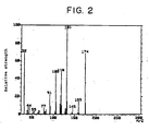
- This chlorinated compound without purifying it, was dissolved in a mixed solvent of 250 ml of diethyl ether and 250 ml of toluene in an argon atmosphere. Fifteen grams of a lithium aluminum hydride was added to the resulting mixture while the mixture was agitated at 0° C. The mixture was agitated for another 3 hours. Thereafter, the mixture was gradually heated to room temperature and agitated for another 6 hours. The aluminum compound was separated from the reaction mixture by filtration, and the filtrate was condensed and purified to give 21 g of the target hydrogenated polysilane compound (Si 6 H 6 ). The MS spectrum thereof is shown in Fig. 2.
- a solution was prepared by dissolving 4 g of the hydrogenated polysilane obtained in the above Synthesis Example 1 in 10 g of toluene. This solution was spin-coated on a quartz substrate on which gold had been vapor-deposited in an argon atmosphere, dried at 150° C in the air, and thermally decomposed at 500°C in the air to give a silicon oxide film having a film thickness of 750 angstrom. This film was a good film on which no film abnormalities such as cracks were observed. When this silicon oxide film was subjected to surface composition analysis by ESCA, only silicon atoms were detected. Further, since the energy in the 2p orbit of this silicon was 104eV, the film was found to be an SiO 2 film.
- a silicon compound solution was prepared by dissolving 5 g of the hydrogenated polysilane obtained in the above Synthesis Example 3 in 10 g of tetrahydronaphthalene.
- This solution ink was pattern-coated on a quartz substrate on which gold had been vapor-deposited in an argon atmosphere by using an ink-jet head comprising a piezoelectric element.
- This substrate was dried at 150° C in the air, thermally decomposed at 500° C in the air, and irradiated with ultraviolet light from a 500-W high-pressure mercury lamp in the air for 10 minutes to give a silicon oxide film having a film thickness of 450 angstrom.
- This film was a good film on which no film abnormalities such as cracks were observed.
- this silicon oxide film was subjected to surface composition analysis by ESCA, only silicon atoms were detected. Further, since the energy in the 2p orbit of this silicon was 104eV, the film was found to be an SiO 2 film.
- a solution was prepared by dissolving a mixture of 2 g of the hydrogenated polysilane compound obtained in the above Synthesis Example 1, 2 g of the hydrogenated polysilane compound obtained in Synthesis Example 2 and 2 g of the hydrogenated polysilane compound obtained in Synthesis Example 3 in 12 g of toluene.
- This solution ink was dip-coated on a polyimide film in an argon atmosphere. The solvent was removed from the substrate, which was then dried at 100° C to obtain a hydrogenated polysilane film having a film thickness of 1,500 angstrom.
- This polysilane film was irradiated with an XeCl excimer laser having a wavelength of 308 nm at an intensity of 300 mJ/cm 2 in the air to give a silicon oxide film having a film thickness of 1,400 angstrom.
- This film was a good film on which no film abnormalities such as cracks were observed.
- this silicon oxide film was subjected to surface composition analysis by ESCA, only silicon atoms were detected. Further, since the energy in the 2p orbit of this silicon was 104eV, the film was found to be an SiO 2 film.
- the etching speed (at the ratio HF/H 2 O of 1/200) of the silicon oxide film obtained in Example 1 was measured, it was 200 angstrom/min.
- the etching speed was 500 angstrom/min.
- the silanol compound obtained by partially hydrolyzing a tetraethoxysilane in ethanol and heated to be in a sol state was spin-coated on a quartz substrate on which gold had been vapor-deposited.
- the substrate was then heat-treated at 200° C for an hour to obtain a 3,000-angstrom silicon oxide film.
- the film had a number of fine cracks.
- a process for forming a silicon oxide film by employing a new material and process using the addition reaction of oxygen which is different from a process for forming a silicon oxide film by a condensation reaction such as the conventionally used sol-gel process.
- a condensation reaction such as the conventionally used sol-gel process.
- the generation of powder at the time of forming a silicon oxide film can be prevented and no expensive apparatus is required because it does not employ a large-scale vacuum process.
- a film can be easily formed on a substrate with a large area, and since a pattern which is directly pattern-coated using an ink-jet process or the like can be converted into a silicon oxide film, a silicon oxide film pattern can be formed without going through processes of photolithography and etching. Consequently, it is made possible by the present invention to produce semiconductor devices such as LSI, thin-film transistor, photoelectric converter, photosensitive body and the like by an energy-efficient process.
Abstract
Description
Claims (6)
- A process for forming a silicon oxide film, comprising:(1) forming a coating film from a polysilane compound represented by the formula SinRm (wherein n is an integer of 3 or more, m is an integer of n to 2n+2, and a plurality of R's independently represent a hydrogen atom or an alkyl group), and(2) oxidizing the coating film by at least one oxidant selected from the group consisting of oxygen and ozone to convert it into the silicon oxide film.
- The process of claim 1, wherein the formation of the coating film from the polysilane compound in the step (1) is conducted using a solution composition obtained by dissolving the polysilane compound in a solvent.
- The process of claim 2, wherein the solvent is at least one selected from the group consisting of hydrocarbon solvents, ether solvents and aprotic solvents.
- The process of claim 1, wherein the oxidization of the coating film in the step (2) is conducted together with heat treatment, radiation treatment or steam treatment.
- The process of claim 1, wherein the oxidization in the step (2) is conducted while heat treatment is conducted in the air at temperatures of 100 to 800° C.
- The process of claim 1, wherein the oxidization in the step (2) is conducted while radiation is irradiated in the air at temperatures of 15 to 500° C.
Applications Claiming Priority (3)
| Application Number | Priority Date | Filing Date | Title |
|---|---|---|---|
| JP8854399 | 1999-03-30 | ||
| JP8854399 | 1999-03-30 | ||
| PCT/JP2000/001961 WO2000059022A1 (en) | 1999-03-30 | 2000-03-29 | Process for the formation of silicon oxide films |
Publications (2)
| Publication Number | Publication Date |
|---|---|
| EP1087433A1 true EP1087433A1 (en) | 2001-03-28 |
| EP1087433A4 EP1087433A4 (en) | 2001-08-16 |
Family
ID=13945775
Family Applications (1)
| Application Number | Title | Priority Date | Filing Date |
|---|---|---|---|
| EP00912923A Withdrawn EP1087433A4 (en) | 1999-03-30 | 2000-03-29 | Process for the formation of silicon oxide films |
Country Status (6)
| Country | Link |
|---|---|
| US (1) | US6517911B1 (en) |
| EP (1) | EP1087433A4 (en) |
| KR (1) | KR100702555B1 (en) |
| CN (1) | CN1297578A (en) |
| TW (1) | TWI234820B (en) |
| WO (1) | WO2000059022A1 (en) |
Cited By (9)
| Publication number | Priority date | Publication date | Assignee | Title |
|---|---|---|---|---|
| EP1134224A2 (en) * | 2000-03-13 | 2001-09-19 | JSR Corporation | Cyclosilane compound, and solution composition and process for forming a silicon film |
| WO2002099864A1 (en) * | 2001-05-31 | 2002-12-12 | Infineon Technologies, Ag | Method for removing polysilane from a semiconductor without stripping |
| EP1284306A3 (en) * | 2001-08-14 | 2004-05-19 | JSR Corporation | Silane composition, silicon film forming method and solar cell production method |
| US7422708B2 (en) | 2003-07-08 | 2008-09-09 | Kovio, Inc. | Compositions for forming a semiconducting and/or silicon-containing film, and structures formed therefrom |
| US7485691B1 (en) | 2004-10-08 | 2009-02-03 | Kovio, Inc | Polysilane compositions, methods for their synthesis and films formed therefrom |
| US7498015B1 (en) | 2004-02-27 | 2009-03-03 | Kovio, Inc. | Method of making silane compositions |
| DE102010030696A1 (en) * | 2010-06-30 | 2012-01-05 | Evonik Degussa Gmbh | Modification of silicon layers from silane-containing formulations |
| US8092867B2 (en) | 2006-10-06 | 2012-01-10 | Kovio, Inc. | Silicon polymers, methods of polymerizing silicon compounds, and methods of forming thin films from such silicon polymers |
| US9336925B1 (en) | 2008-11-26 | 2016-05-10 | Thin Film Electronics Asa | Siloxanes, doped siloxanes, methods for their synthesis, compositions containing the same, and films formed therefrom |
Families Citing this family (27)
| Publication number | Priority date | Publication date | Assignee | Title |
|---|---|---|---|---|
| TW570876B (en) * | 2001-05-11 | 2004-01-11 | Toyo Seikan Kaisha Ltd | Silicon oxide film |
| JP2003055556A (en) * | 2001-08-14 | 2003-02-26 | Jsr Corp | Method for forming silicon film or silicon oxide film and composition for them |
| JP4548567B2 (en) * | 2001-09-19 | 2010-09-22 | Jsr株式会社 | Method for forming silicon oxide film |
| KR101227664B1 (en) * | 2002-01-31 | 2013-01-29 | 도소 가부시키가이샤 | Material for insulation film comprising organosilane compound, its manufacturing method and semiconductor device |
| CN100415752C (en) * | 2002-01-31 | 2008-09-03 | 东粟株式会社 | Insulating film material containing an organic silane compound, its production method and semiconductor device |
| CN100397245C (en) * | 2002-07-23 | 2008-06-25 | 大阪瓦斯株式会社 | Electrophotographic photoreceptor and electrophoto- graphic apparatus equipped with the same |
| US20050196974A1 (en) * | 2004-03-02 | 2005-09-08 | Weigel Scott J. | Compositions for preparing low dielectric materials containing solvents |
| US8211396B1 (en) | 2004-09-24 | 2012-07-03 | Kovio, Inc. | Heterocyclic semiconductor precursor compounds, compositions containing the same, and methods of making such compounds and compositions |
| US7314513B1 (en) * | 2004-09-24 | 2008-01-01 | Kovio, Inc. | Methods of forming a doped semiconductor thin film, doped semiconductor thin film structures, doped silane compositions, and methods of making such compositions |
| US7674926B1 (en) | 2004-10-01 | 2010-03-09 | Kovio, Inc. | Dopant group-substituted semiconductor precursor compounds, compositions containing the same, and methods of making such compounds and compositions |
| WO2007044429A2 (en) | 2005-10-05 | 2007-04-19 | Nanogram Corporation | Linear and cross-linked high molecular weight polysilanes, polygermanes, and copolymers thereof, compositions containing the same, and methods of making and using such compounds and compositions |
| US7691691B1 (en) | 2006-05-23 | 2010-04-06 | Kovio, Inc. | Semiconductor device and methods for making the same |
| US20080029046A1 (en) * | 2006-05-25 | 2008-02-07 | Welles Robert D | Hot water reclaimer |
| CN101455121B (en) * | 2006-06-14 | 2012-06-27 | 株式会社半导体能源研究所 | Method for manufacturing semiconductor device |
| JP2007142451A (en) * | 2007-01-22 | 2007-06-07 | Nec Corp | Insulating layer, insulating layer pattern, thin film transistor, liquid crystal display, and liquid pattern formation device |
| US20080216958A1 (en) * | 2007-03-07 | 2008-09-11 | Novellus Systems, Inc. | Plasma Reaction Apparatus Having Pre-Seasoned Showerheads and Methods for Manufacturing the Same |
| US20080216302A1 (en) * | 2007-03-07 | 2008-09-11 | Novellus Systems, Inc. | Methods utilizing organosilicon compounds for manufacturing pre-seasoned components and plasma reaction apparatuses having pre-seasoned components |
| WO2009026126A2 (en) * | 2007-08-17 | 2009-02-26 | Ndsu Research Foundation | Convergent-divergent-convergent nozzle focusing of aerosol particles for micron-scale direct writing |
| JP2008143782A (en) * | 2008-02-08 | 2008-06-26 | Jsr Corp | Method for manufacturing solar cell |
| JP5618599B2 (en) * | 2009-04-10 | 2014-11-05 | 独立行政法人科学技術振興機構 | Pattern formation method |
| KR101648867B1 (en) | 2009-06-02 | 2016-08-17 | 삼성전자주식회사 | Manufacturing Method of Si Film using Si Solution Process |
| KR101175405B1 (en) * | 2009-09-03 | 2012-08-20 | 신동윤 | Method for preparing polysilanes, polysilanes prepared thereby, dehydrogenation catalyst used for the method, method for manufacturing amorphous silicon thin film using the polysilanes |
| US8624049B2 (en) * | 2010-01-18 | 2014-01-07 | Kovio, Inc. | Dopant group-substituted semiconductor precursor compounds, compositions containing the same, and methods of making such compounds and compositions |
| JP2011168870A (en) * | 2010-02-22 | 2011-09-01 | Ulvac Japan Ltd | Film-deposition device and maintenance method |
| JP5442572B2 (en) | 2010-09-28 | 2014-03-12 | 株式会社日立ハイテクサイエンス | Charged particle beam apparatus, thin film manufacturing method, defect correcting method, and device manufacturing method |
| US8534524B2 (en) * | 2010-10-08 | 2013-09-17 | Gtech Corporation | Perforated ticket dispensing machine |
| US10858260B2 (en) * | 2014-12-15 | 2020-12-08 | Evonik Operations Gmbh | Method for producing perhalogenated hexasilane anion and method for producing a cyclic silane compound |
Citations (1)
| Publication number | Priority date | Publication date | Assignee | Title |
|---|---|---|---|---|
| US5445894A (en) * | 1991-04-22 | 1995-08-29 | Dow Corning Corporation | Ceramic coatings |
Family Cites Families (8)
| Publication number | Priority date | Publication date | Assignee | Title |
|---|---|---|---|---|
| JPH03242933A (en) * | 1990-02-21 | 1991-10-29 | Toagosei Chem Ind Co Ltd | Manufacture of semiconductor device, and semiconductor device |
| JPH04334551A (en) | 1991-05-10 | 1992-11-20 | Tonen Corp | Polymerization catalyst of hydrosilane |
| JPH05295563A (en) * | 1992-04-23 | 1993-11-09 | Kansai Shin Gijutsu Kenkyusho:Kk | Metallic material having coating film and its production |
| JP3000825B2 (en) | 1993-07-14 | 2000-01-17 | 株式会社村田製作所 | Ceramic electronic components |
| JPH07142470A (en) * | 1993-11-15 | 1995-06-02 | Toshiba Corp | Deposition of insulating film |
| JP3139263B2 (en) * | 1994-02-23 | 2001-02-26 | 富士電機株式会社 | Method for forming protective film of semiconductor device |
| JPH0870000A (en) * | 1994-08-29 | 1996-03-12 | Fujitsu Ltd | Fabrication of semiconductor device |
| JP5445894B2 (en) * | 2008-03-14 | 2014-03-19 | 国立大学法人 筑波大学 | Terahertz band electromagnetic wave oscillator with directivity |
-
2000
- 2000-03-29 EP EP00912923A patent/EP1087433A4/en not_active Withdrawn
- 2000-03-29 TW TW089105752A patent/TWI234820B/en not_active IP Right Cessation
- 2000-03-29 WO PCT/JP2000/001961 patent/WO2000059022A1/en active IP Right Grant
- 2000-03-29 US US09/700,726 patent/US6517911B1/en not_active Expired - Fee Related
- 2000-03-29 CN CN00800470A patent/CN1297578A/en active Pending
- 2000-03-29 KR KR1020007013458A patent/KR100702555B1/en not_active IP Right Cessation
Patent Citations (1)
| Publication number | Priority date | Publication date | Assignee | Title |
|---|---|---|---|---|
| US5445894A (en) * | 1991-04-22 | 1995-08-29 | Dow Corning Corporation | Ceramic coatings |
Non-Patent Citations (4)
| Title |
|---|
| PATENT ABSTRACTS OF JAPAN vol. 018, no. 101 (C-1168), 18 February 1994 (1994-02-18) -& JP 05 295563 A (KANSAI SHIN GIJUTSU KENKYUSHO:KK), 9 November 1993 (1993-11-09) * |
| PATENT ABSTRACTS OF JAPAN vol. 1995, no. 09, 31 October 1995 (1995-10-31) -& JP 07 142470 A (TOSHIBA CORP), 2 June 1995 (1995-06-02) * |
| PATENT ABSTRACTS OF JAPAN vol. 1996, no. 01, 31 January 1996 (1996-01-31) -& JP 07 235532 A (FUJI ELECTRIC CO LTD), 5 September 1995 (1995-09-05) * |
| See also references of WO0059022A1 * |
Cited By (31)
| Publication number | Priority date | Publication date | Assignee | Title |
|---|---|---|---|---|
| EP1134224A3 (en) * | 2000-03-13 | 2003-01-15 | JSR Corporation | Cyclosilane compound, and solution composition and process for forming a silicon film |
| EP1134224A2 (en) * | 2000-03-13 | 2001-09-19 | JSR Corporation | Cyclosilane compound, and solution composition and process for forming a silicon film |
| WO2002099864A1 (en) * | 2001-05-31 | 2002-12-12 | Infineon Technologies, Ag | Method for removing polysilane from a semiconductor without stripping |
| US6740594B2 (en) | 2001-05-31 | 2004-05-25 | Infineon Technologies Ag | Method for removing carbon-containing polysilane from a semiconductor without stripping |
| EP1284306A3 (en) * | 2001-08-14 | 2004-05-19 | JSR Corporation | Silane composition, silicon film forming method and solar cell production method |
| US7067069B2 (en) | 2001-08-14 | 2006-06-27 | Jsr Corporation | Silane composition, silicon film forming method and solar cell production method |
| US7173180B2 (en) | 2001-08-14 | 2007-02-06 | Jsr Corporation | Silane composition, silicon film forming method and solar cell production method |
| CN100392008C (en) * | 2001-08-14 | 2008-06-04 | Jsr株式会社 | Silane composition, silicon film forming method and manufacture of solar cells |
| US7553545B2 (en) | 2003-07-08 | 2009-06-30 | Kovio, Inc. | Compositions and methods for forming a semiconducting and/or silicon-containing film, and structures formed therefrom |
| US7422708B2 (en) | 2003-07-08 | 2008-09-09 | Kovio, Inc. | Compositions for forming a semiconducting and/or silicon-containing film, and structures formed therefrom |
| US7879696B2 (en) | 2003-07-08 | 2011-02-01 | Kovio, Inc. | Compositions and methods for forming a semiconducting and/or silicon-containing film, and structures formed therefrom |
| US7799302B1 (en) | 2004-02-27 | 2010-09-21 | Kovio, Inc. | Silane compositions, methods of making the same, method for forming a semiconducting and/or silicon-containing film, and thin film structures formed therefrom |
| US7498015B1 (en) | 2004-02-27 | 2009-03-03 | Kovio, Inc. | Method of making silane compositions |
| US8603426B1 (en) | 2004-02-27 | 2013-12-10 | Kovio, Inc. | Method of making a silicon-containing film |
| US8367031B1 (en) | 2004-02-27 | 2013-02-05 | Kovio, Inc. | Silane compositions, methods of making the same, method for forming a semiconducting and/or silicon-containing film, and thin film structures formed therefrom |
| US8124040B1 (en) | 2004-02-27 | 2012-02-28 | Kovio, Inc. | Methods of making silane compositions |
| US7951892B1 (en) | 2004-10-08 | 2011-05-31 | Kovio, Inc. | Doped polysilanes, compositions containing the same, methods for making the same, and films formed therefrom |
| US7491782B1 (en) | 2004-10-08 | 2009-02-17 | Kovio, Inc. | Polysilane compositions, methods for their synthesis and films formed therefrom |
| US7723457B1 (en) | 2004-10-08 | 2010-05-25 | Kovio, Inc. | Polysilane compositions, methods for their synthesis and films formed therefrom |
| US8455604B1 (en) | 2004-10-08 | 2013-06-04 | Kovio, Inc. | Polysilane compositions, methods for their synthesis and films formed therefrom |
| US8057865B1 (en) | 2004-10-08 | 2011-11-15 | Kovio, Inc. | Polysilane compositions, methods for their synthesis and films formed therefrom |
| US7485691B1 (en) | 2004-10-08 | 2009-02-03 | Kovio, Inc | Polysilane compositions, methods for their synthesis and films formed therefrom |
| US8236916B1 (en) | 2004-10-08 | 2012-08-07 | Kovio, Inc. | Polysilane compositions, methods for their synthesis and films formed therefrom |
| US8242227B2 (en) | 2004-10-08 | 2012-08-14 | Kovio, Inc. | Doped polysilanes, compositions containing the same, methods for making the same, and films formed therefrom |
| US8092867B2 (en) | 2006-10-06 | 2012-01-10 | Kovio, Inc. | Silicon polymers, methods of polymerizing silicon compounds, and methods of forming thin films from such silicon polymers |
| US8461284B2 (en) | 2006-10-06 | 2013-06-11 | Kovio, Inc. | Silicon polymers, methods of polymerizing silicon compounds, and methods of forming thin films from such silicon polymers |
| US8846507B2 (en) | 2006-10-06 | 2014-09-30 | Thin Film Electronics Asa | Silicon polymers, methods of polymerizing silicon compounds, and methods of forming thin films from such silicon polymers |
| US9336925B1 (en) | 2008-11-26 | 2016-05-10 | Thin Film Electronics Asa | Siloxanes, doped siloxanes, methods for their synthesis, compositions containing the same, and films formed therefrom |
| US9704713B1 (en) | 2008-11-26 | 2017-07-11 | Thin Film Electronics Asa | Siloxanes, doped siloxanes, methods for their synthesis, compositions containing the same, and films formed therefrom |
| WO2012000815A1 (en) | 2010-06-30 | 2012-01-05 | Evonik Degussa Gmbh | Modification of silicon layers formed from silane-containing formulations |
| DE102010030696A1 (en) * | 2010-06-30 | 2012-01-05 | Evonik Degussa Gmbh | Modification of silicon layers from silane-containing formulations |
Also Published As
| Publication number | Publication date |
|---|---|
| WO2000059022A1 (en) | 2000-10-05 |
| KR100702555B1 (en) | 2007-04-04 |
| CN1297578A (en) | 2001-05-30 |
| TWI234820B (en) | 2005-06-21 |
| KR20010052442A (en) | 2001-06-25 |
| US6517911B1 (en) | 2003-02-11 |
| EP1087433A4 (en) | 2001-08-16 |
Similar Documents
| Publication | Publication Date | Title |
|---|---|---|
| US6517911B1 (en) | Process for the formation of silicon oxide films | |
| US7173180B2 (en) | Silane composition, silicon film forming method and solar cell production method | |
| US6527847B1 (en) | Coating composition | |
| KR100562815B1 (en) | Solution Composition for Forming a Silicon Film and Method for Preparing the Silicon Film | |
| JP4042327B2 (en) | Thin film transistor manufacturing method | |
| KR100436319B1 (en) | Method for forming silicon film | |
| JP2003055556A (en) | Method for forming silicon film or silicon oxide film and composition for them | |
| JP2003171556A (en) | Method for forming silicon film and composition therefor | |
| JP4462394B2 (en) | Silicon film pattern forming method | |
| JP2002246384A (en) | Method of forming silicon oxide film and composition used for forming the same | |
| JP4419357B2 (en) | Silane composition and method for producing solar cell using the same | |
| JP4518222B2 (en) | Silylcyclopentasilane and its uses | |
| JP4748288B2 (en) | Composition containing spiro [4.4] nonasilane | |
| JP4548567B2 (en) | Method for forming silicon oxide film | |
| WO2004065659A1 (en) | Composition for forming silicon·aluminum film, silicon·aluminum film and method for forming the same | |
| JPH11130867A (en) | Improved organosilicon nanocluster and its production | |
| JP2008143782A (en) | Method for manufacturing solar cell | |
| JP2001058996A (en) | Norbornyl group-containing silicon compound, coating composition and production of silicon film |
Legal Events
| Date | Code | Title | Description |
|---|---|---|---|
| PUAI | Public reference made under article 153(3) epc to a published international application that has entered the european phase |
Free format text: ORIGINAL CODE: 0009012 |
|
| AK | Designated contracting states |
Kind code of ref document: A1 Designated state(s): AT BE CH CY DE DK ES FI FR GB GR IE IT LI LU MC NL PT SE |
|
| 17P | Request for examination filed |
Effective date: 20010131 |
|
| A4 | Supplementary search report drawn up and despatched |
Effective date: 20010629 |
|
| AK | Designated contracting states |
Kind code of ref document: A4 Designated state(s): AT BE CH CY DE DK ES FI FR GB GR IE IT LI LU MC NL PT SE |
|
| RAP1 | Party data changed (applicant data changed or rights of an application transferred) |
Owner name: JSR CORPORATION |
|
| RBV | Designated contracting states (corrected) |
Designated state(s): DE FR GB NL |
|
| 17Q | First examination report despatched |
Effective date: 20041008 |
|
| STAA | Information on the status of an ep patent application or granted ep patent |
Free format text: STATUS: THE APPLICATION IS DEEMED TO BE WITHDRAWN |
|
| 18D | Application deemed to be withdrawn |
Effective date: 20140410 |